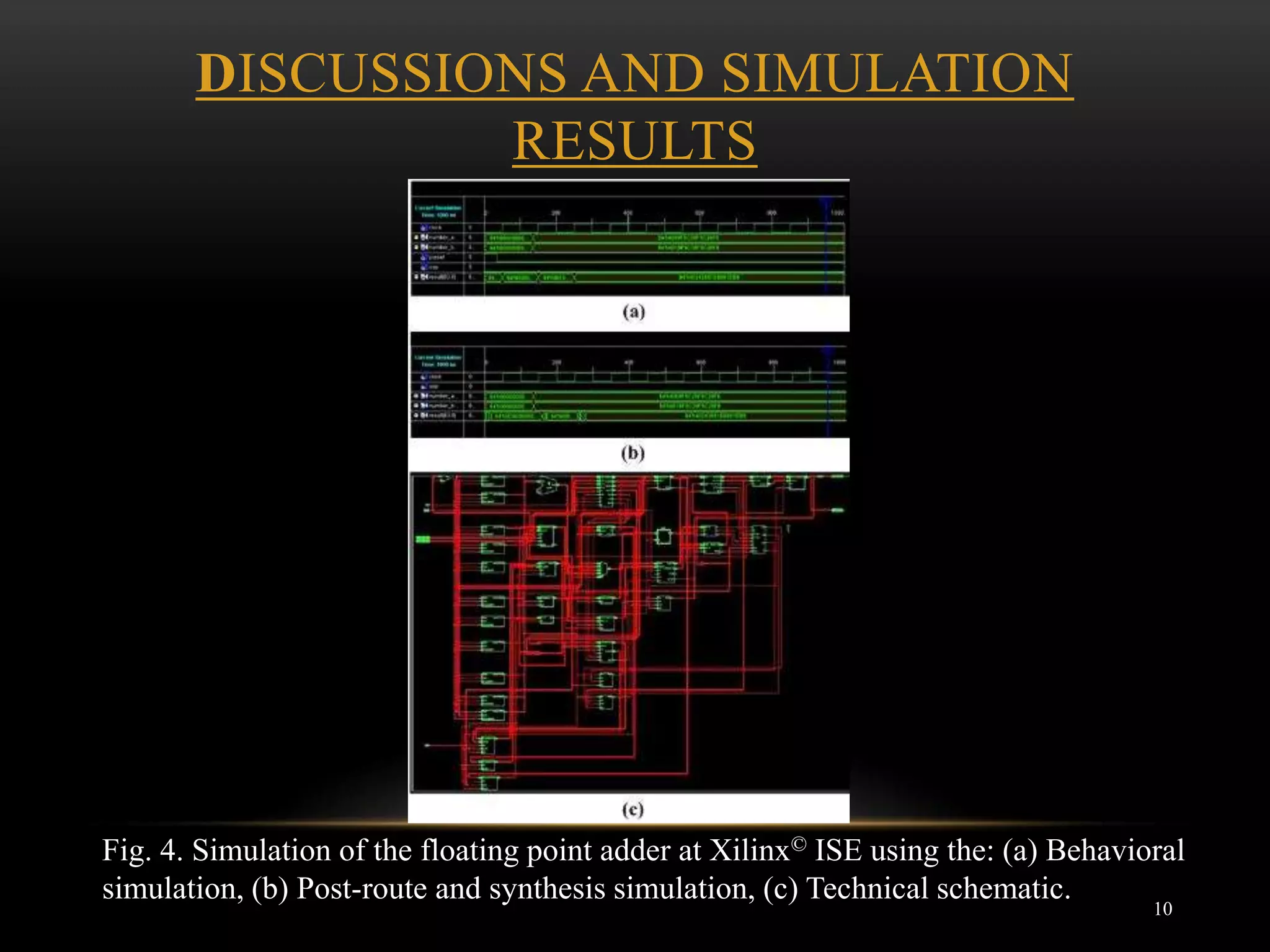
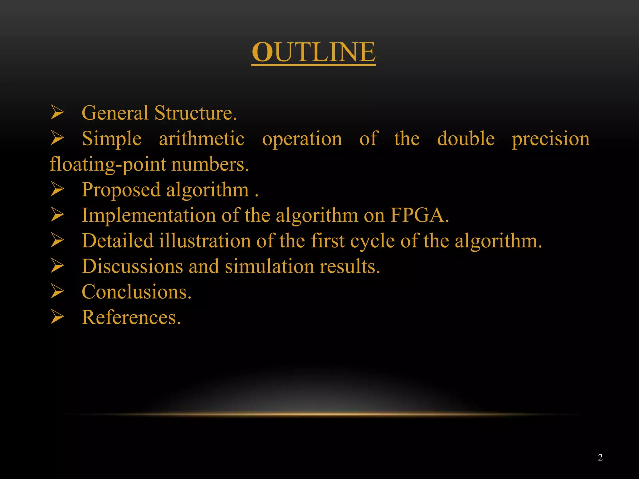
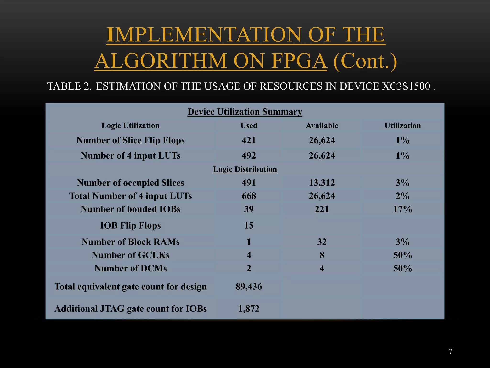
This document describes an FPGA implementation of a double precision IEEE floating point adder. It outlines the general structure of IEEE 754 double precision numbers, describes the simple arithmetic operation of adding two such numbers, and proposes a two stage pipelined algorithm to perform the addition. It then discusses implementing the algorithm on FPGA devices, providing resource usage estimates and illustrations of the first two cycles of the algorithm. Simulation results are presented and the conclusions discuss the benefits of this technique for performing floating point additions with low latency.


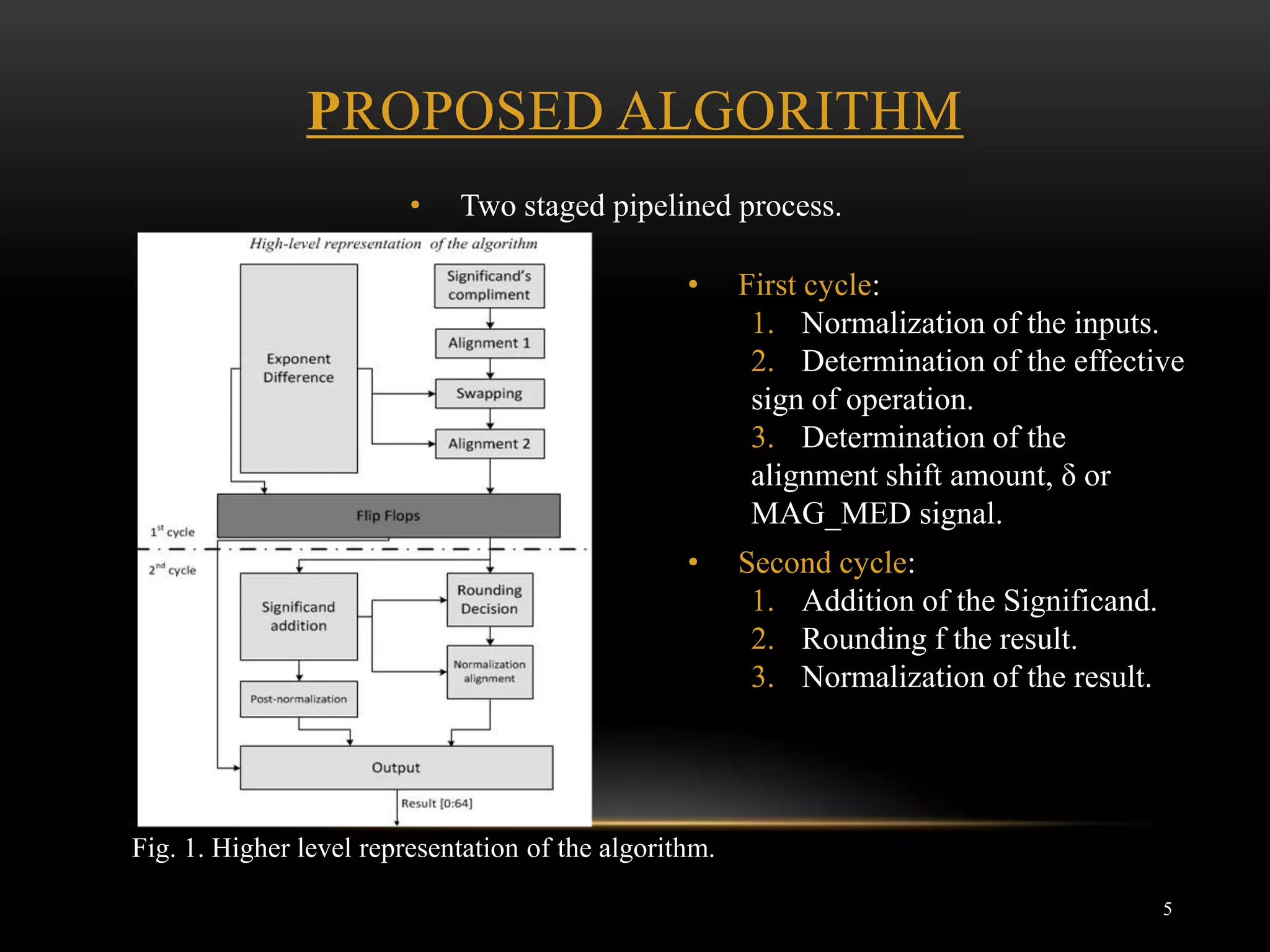

![DETAILED ILLUSTRATION OF THE
FIRST CYCLE OF THE ALGORITHM
FB[0:52]
FA[0:52]
SA
SOP
SB
EA EB
FLIP FLOPS ONE’S COMPLEMENT S.EFF
FAO[0:52] FBO[0:52]
ADDER (5) ADDER (7)
PRESHIFT
SIGN_MED 1 0
XOR FSOP[-1:53] MUX
XOR
0 1
MUX
MAG_MED[5:0] SHIFT(63)
ORTREE SHIFT(65)
FL[0:52]
0 1
IS_BIG MUX SHIFT(1)
FSOPA[-1:116] FLP[-1:52]
SIGN_BIG
Fig. 2. Block level representation of the 1st cycle of the algorithm.
8](https://image.slidesharecdn.com/fpgabasedimplementationofadoubleprecisionieeefloating-pointadder-130106081449-phpapp01/75/Fpga-based-implementation-of-a-double-precision-ieee-floating-point-adder-8-2048.jpg)