Download as PDF, PPTX
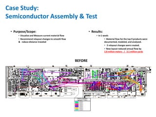
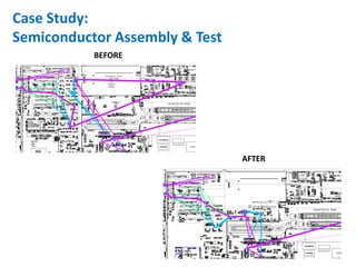
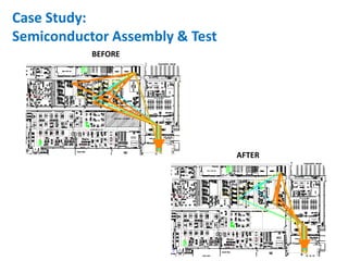
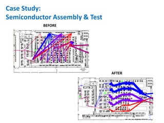
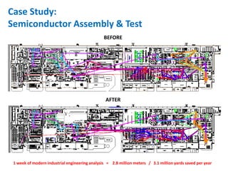
The document describes a case study where a semiconductor assembly facility was analyzed to visualize and measure current material flows, recommend layout changes to smooth flows and reduce distances traveled. Within a week, material flows for the top 9 products were documented, modeled and analyzed, and 3 relayout changes were proposed. The new layout was estimated to reduce annual material flow by 2.8 million meters or 3.1 million yards.


![03_August_2016_Richard_Bailey_Resume[1]](https://cdn.slidesharecdn.com/ss_thumbnails/e5274ef5-9684-4ad9-ab7b-525cb01b04c4-170302134408-thumbnail.jpg?width=640&height=640&fit=bounds)


