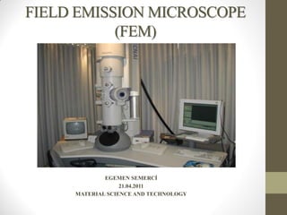
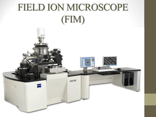
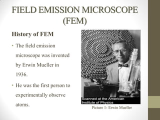
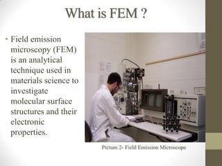
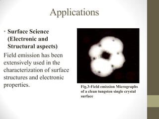
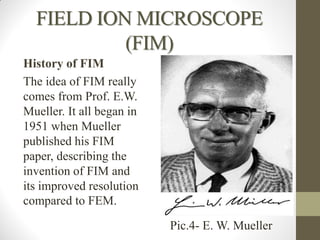
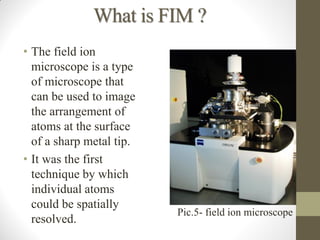
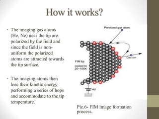
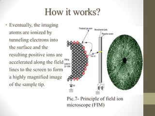
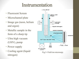
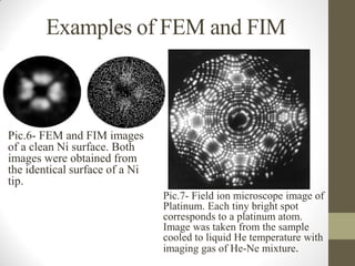
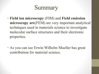
FIELD EMISSION MICROSCOPE
(FEM)
EGEMEN SEMERCİ
21.04.2011
MATERIAL SCIENCE AND TECHNOLOGY
FIELD ION MICROSCOPE
(FIM)
Presentation Content
• History of FEM
• What is FEM ?
• How it works ?
• Instrumentation
• Working conditions
• Applications
• Same content for
FIM
• Examples of FEM
and FIM
• Summary
• References
FIELD EMISSION MICROSCOPE
(FEM)
History of FEM
• The field emission
microscope was invented
by Erwin Mueller in
1936.
• He was the first person to
experimentally observe
atoms. Picture 1- Erwin Mueller
What is FEM ?
• Field emission
microscopy (FEM)
is an analytical
technique used in
materials science to
investigate
molecular surface
structures and their
electronic
properties.
Picture 2- Field Emission Microscope
What is FEM ?
• FEM was one of the first surface analysis
instruments that approached near-atomic resolution.
• This instrument approached to view a surface on a
scale of atomic dimensions and yet simultaneously
allowed one to follow rapid changes at the surface.
How it works?
In its simplest form, FEM
consist of a sharp needle emitter
and a fluorescent screen as
shown in Fig. 1. By applying
negative field to the emitter,
electrons are emitted from the
surface of the emitter to the
direction of the screen. The
image contrast appears due to
the difference in current
densities of electron, which
originated from the difference in
work functions and electric field
on the emitter surface
Instrumentation
• Fluorescent Screen
• Metallic sample in
the form of a sharp
tip
• Ultra high vacuum
(UHV), pump
• Power supply
Fig.2:FEM experimental
set-up
Working conditions
• Requires a very good vacuum (ultra high
vacuum)
• Emission is not due to the clean surface.
• No vibrations
• Tip materials can tolerate the high
electrostatic fields and have high melting
points
Applications
• Surface Science
(Electronic and
Structural aspects)
Field emission has been
extensively used in the
characterization of surface
structures and electronic
properties. Fig.3-Field emission Micrographs
of a clean tungsten single crystal
surface
FIELD ION MICROSCOPE
(FIM)
History of FIM
The idea of FIM really
comes from Prof. E.W.
Mueller. It all began in
1951 when Mueller
published his FIM
paper, describing the
invention of FIM and
its improved resolution
compared to FEM.
Pic.4- E. W. Mueller
What is FIM ?
• The field ion
microscope is a type
of microscope that
can be used to image
the arrangement of
atoms at the surface
of a sharp metal tip.
• It was the first
technique by which
individual atoms
could be spatially
resolved.
Pic.5- field ion microscope
How it works?
• The imaging gas atoms
(He, Ne) near the tip are
polarized by the field and
since the field is non-
uniform the polarized
atoms are attracted towards
the tip surface.
• The imaging atoms then
lose their kinetic energy
performing a series of hops
and accommodate to the tip
temperature.
Pic.6- FIM image formation
process.
How it works?
• Eventually, the imaging
atoms are ionized by
tunneling electrons into
the surface and the
resulting positive ions are
accelerated along the field
lines to the screen to form
a highly magnified image
of the sample tip.
Pic.7- Principle of field ion
microscope (FIM)
Instrumentation
• Fluoresent Screen
• Microchannel plate
• Image gas (neon, helium
and argon)
• Metallic sample in the
form of a sharp tip
• Ultra high vacuum
(UHV), pump
• Power supply
• Cooling agent (liquid
nitrogen)
Fig.3- Field ion microscpy
Working conditions
• FIM like Field Emission Microscopy (FEM) . Both
have same working conditions.
However, there are some essential differences as
follows:
• The tip potential is positive.
• The chamber is filled with a imaging gas (typically,
He or Ne at 10-5 to 10-3 Torr).
• The tip is cooled to low temperatures (~20-80K).
Applications
• FIM has been used to study dynamical behavior of
surfaces and the behavior of adatoms on surfaces.
The problems studied include:
• Surface diffusion of adatoms ,
• Adatom-adatom interactions,
• Step motion,
• Equilibrium crystal shape, etc.
Examples of FEM and FIM
Pic.6- FEM and FIM images
of a clean Ni surface. Both
images were obtained from
the identical surface of a Ni
tip.
Pic.7- Field ion microscope image of
Platinum. Each tiny bright spot
corresponds to a platinum atom.
Image was taken from the sample
cooled to liquid He temperature with
imaging gas of He-Ne mixture.
Summary
• Field ion microscopy (FIM) and Field emission
microscopy are(FEM) are very important analytical
techniques used in materials science to investigate
molecular surface structures and their electronic
properties.
• As you can see Erwin Wilhelm Mueller has great
contribution for material science.
References
1) http://en.wikipedia.org/wiki/Erwin_Wilhelm_M%C3%BCller
2) http://physics.unipune.ernet.in/~fem/intro-fem.htm
3) http://physics.unipune.ernet.in/~fem/intro-fim.htm
4) http://en.wikipedia.org/wiki/Field_ion_microscope
5) http://en.wikipedia.org/wiki/Adatoms
6) http://www.nims.go.jp/apfim/fim.html
7) http://piercing-intim.com/warrents-platinum-record
8) http://www.nims.go.jp/apfim/FEM.html
9) http://en.wikipedia.org/wiki/Field_emission_microscopy
10) http://www.wadsworth.org/rvbc/f20.jpg
11) http://www.nims.go.jp/apfim/FEM.html
12) http://www.google.com.tr/imgres?imgurl=http://www.nims.go.jp/ap
fim/gif/FIMschematic.gif&imgrefurl
13) http://en.wikipedia.org/wiki/File:FIMtip.JPG
14) http://www.sustainability.rit.edu/nanopower/labs/fiedl_emission.jpg
THANKS FOR YOUR
ATTENTION

Field ion microscope and field emision microscope

  • 1.
    FIELD EMISSION MICROSCOPE (FEM) EGEMENSEMERCİ 21.04.2011 MATERIAL SCIENCE AND TECHNOLOGY
  • 2.
  • 3.
    Presentation Content • Historyof FEM • What is FEM ? • How it works ? • Instrumentation • Working conditions • Applications • Same content for FIM • Examples of FEM and FIM • Summary • References
  • 4.
    FIELD EMISSION MICROSCOPE (FEM) Historyof FEM • The field emission microscope was invented by Erwin Mueller in 1936. • He was the first person to experimentally observe atoms. Picture 1- Erwin Mueller
  • 5.
    What is FEM? • Field emission microscopy (FEM) is an analytical technique used in materials science to investigate molecular surface structures and their electronic properties. Picture 2- Field Emission Microscope
  • 6.
    What is FEM? • FEM was one of the first surface analysis instruments that approached near-atomic resolution. • This instrument approached to view a surface on a scale of atomic dimensions and yet simultaneously allowed one to follow rapid changes at the surface.
  • 7.
    How it works? Inits simplest form, FEM consist of a sharp needle emitter and a fluorescent screen as shown in Fig. 1. By applying negative field to the emitter, electrons are emitted from the surface of the emitter to the direction of the screen. The image contrast appears due to the difference in current densities of electron, which originated from the difference in work functions and electric field on the emitter surface
  • 8.
    Instrumentation • Fluorescent Screen •Metallic sample in the form of a sharp tip • Ultra high vacuum (UHV), pump • Power supply Fig.2:FEM experimental set-up
  • 9.
    Working conditions • Requiresa very good vacuum (ultra high vacuum) • Emission is not due to the clean surface. • No vibrations • Tip materials can tolerate the high electrostatic fields and have high melting points
  • 10.
    Applications • Surface Science (Electronicand Structural aspects) Field emission has been extensively used in the characterization of surface structures and electronic properties. Fig.3-Field emission Micrographs of a clean tungsten single crystal surface
  • 11.
    FIELD ION MICROSCOPE (FIM) Historyof FIM The idea of FIM really comes from Prof. E.W. Mueller. It all began in 1951 when Mueller published his FIM paper, describing the invention of FIM and its improved resolution compared to FEM. Pic.4- E. W. Mueller
  • 12.
    What is FIM? • The field ion microscope is a type of microscope that can be used to image the arrangement of atoms at the surface of a sharp metal tip. • It was the first technique by which individual atoms could be spatially resolved. Pic.5- field ion microscope
  • 13.
    How it works? •The imaging gas atoms (He, Ne) near the tip are polarized by the field and since the field is non- uniform the polarized atoms are attracted towards the tip surface. • The imaging atoms then lose their kinetic energy performing a series of hops and accommodate to the tip temperature. Pic.6- FIM image formation process.
  • 14.
    How it works? •Eventually, the imaging atoms are ionized by tunneling electrons into the surface and the resulting positive ions are accelerated along the field lines to the screen to form a highly magnified image of the sample tip. Pic.7- Principle of field ion microscope (FIM)
  • 15.
    Instrumentation • Fluoresent Screen •Microchannel plate • Image gas (neon, helium and argon) • Metallic sample in the form of a sharp tip • Ultra high vacuum (UHV), pump • Power supply • Cooling agent (liquid nitrogen) Fig.3- Field ion microscpy
  • 16.
    Working conditions • FIMlike Field Emission Microscopy (FEM) . Both have same working conditions. However, there are some essential differences as follows: • The tip potential is positive. • The chamber is filled with a imaging gas (typically, He or Ne at 10-5 to 10-3 Torr). • The tip is cooled to low temperatures (~20-80K).
  • 17.
    Applications • FIM hasbeen used to study dynamical behavior of surfaces and the behavior of adatoms on surfaces. The problems studied include: • Surface diffusion of adatoms , • Adatom-adatom interactions, • Step motion, • Equilibrium crystal shape, etc.
  • 18.
    Examples of FEMand FIM Pic.6- FEM and FIM images of a clean Ni surface. Both images were obtained from the identical surface of a Ni tip. Pic.7- Field ion microscope image of Platinum. Each tiny bright spot corresponds to a platinum atom. Image was taken from the sample cooled to liquid He temperature with imaging gas of He-Ne mixture.
  • 19.
    Summary • Field ionmicroscopy (FIM) and Field emission microscopy are(FEM) are very important analytical techniques used in materials science to investigate molecular surface structures and their electronic properties. • As you can see Erwin Wilhelm Mueller has great contribution for material science.
  • 20.
    References 1) http://en.wikipedia.org/wiki/Erwin_Wilhelm_M%C3%BCller 2) http://physics.unipune.ernet.in/~fem/intro-fem.htm 3)http://physics.unipune.ernet.in/~fem/intro-fim.htm 4) http://en.wikipedia.org/wiki/Field_ion_microscope 5) http://en.wikipedia.org/wiki/Adatoms 6) http://www.nims.go.jp/apfim/fim.html 7) http://piercing-intim.com/warrents-platinum-record 8) http://www.nims.go.jp/apfim/FEM.html 9) http://en.wikipedia.org/wiki/Field_emission_microscopy 10) http://www.wadsworth.org/rvbc/f20.jpg 11) http://www.nims.go.jp/apfim/FEM.html 12) http://www.google.com.tr/imgres?imgurl=http://www.nims.go.jp/ap fim/gif/FIMschematic.gif&imgrefurl 13) http://en.wikipedia.org/wiki/File:FIMtip.JPG 14) http://www.sustainability.rit.edu/nanopower/labs/fiedl_emission.jpg
  • 21.