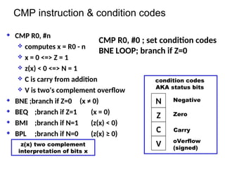
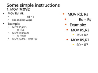
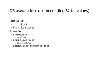
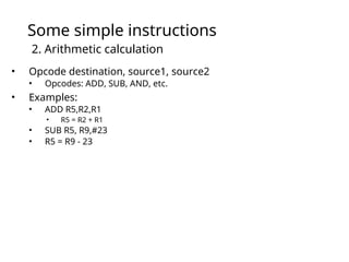
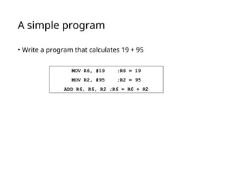
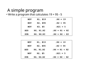
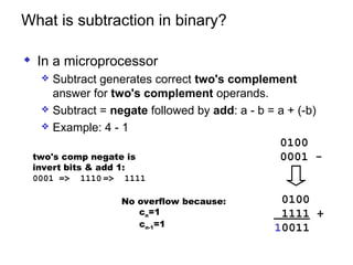
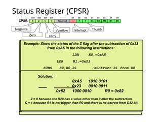
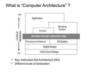
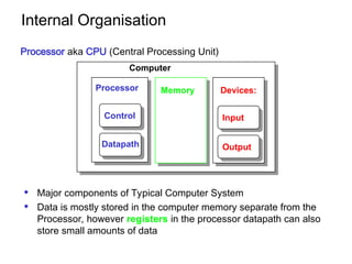
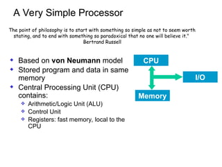
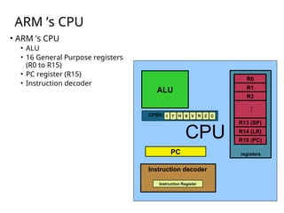
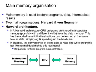
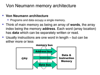
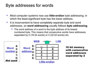
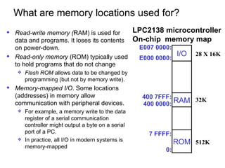
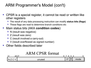
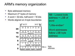
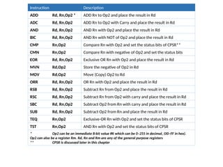
What is “Computer Architecture” ?
INSTRUCTION SET ARCHITECTURE
Operating
System
Processor Architecture I/O System
Digital Design
VLSI Circuit Design
Application
Compiler
Levels
of
Abstraction
low
high
 Key: Instruction Set Architecture (ISA)
 Different levels of abstraction
Internal Organisation
 Major components of Typical Computer System
 Data is mostly stored in the computer memory separate from the
Processor, however registers in the processor datapath can also
store small amounts of data
Processor
Computer
Control
Datapath
Memory Devices:
Input
Output
Processor aka CPU (Central Processing Unit)
A Very Simple Processor
 Based on von Neumann model
 Stored program and data in same
memory
 Central Processing Unit (CPU)
contains:
 Arithmetic/Logic Unit (ALU)
 Control Unit
 Registers: fast memory, local to the
CPU
CPU
Memory
I/O
The point of philosophy is to start with something so simple as not to seem worth
stating, and to end with something so paradoxical that no one will believe it."
Bertrand Russell
ARM ’s CPU
• ARM ’s CPU
• ALU
• 16 General Purpose registers
(R0 to R15)
• PC register (R15)
• Instruction decoder
CPU
PC
ALU
registers
R1
R0
R13 (SP)
R2
…
R14 (LR)
Instruction Register
Instruction decoder
CPSR: I T H S V N C
Z
R15 (PC)
Main memory organisation
 Main memory is used to store programs, data, intermediate
results
 Two main organisations: Harvard & von Neumann
 Harvard architecture.
 In A Harvard architecture CPU programs are stored in a separate
memory (possibly with a different width) from the data memory. This
has the added benefit that instructions can be fetched at the same
time as data, simplifying & speeding up the hardware.
 In practice, the convenience of being able to read and write programs
just like normal data makes this less usual
still popular for fixed program microcontrollers.
CPU
Data
Memory
Instruction
Memory
Von Neumann memory architecture
 Von Neumann architecture
 Programs and data occupy a single memory.
 Think of main memory as being an array of words, the array
index being the memory address. Each word (array location)
has data which can be separately written or read.
 Usually instructions are one word in length – but can be
either more or less
CPU
Data bus
Data &
Instruction
Memory
Address bus
Control bus
memory bus
Memory in detail
 Memory locations store instructions data and
each have unique numeric addresses
 Usually addresses range from 0 up to some
maximum value.
 Memory space is the unique range of possible
memory addresses in a computer system
 We talk about “the address of a memory
location”.
 Each memory location stores a fixed number
of bits of data, normally 8, 16, 32 or 64
 We write mem8[100], mem16[100] to indicate
the value of the 8 or 16 bits with memory
address 100 etc
0 02E
machine
code
2 02F
1 030
7 000
--
0AA0
0110
0BB0
--
--
000
001
002
003
004
005
006
02E
02F
030
...
Byte addresses for words
 Most computer systems now use little-endian byte addressing, in
which the least-significant byte has the lower address.
 It is inconvenient to have completely separate byte and word
addresses, so word addressing usually follows byte addressing.
 The word address of a word is the byte address of its lowest
numbered byte. This means that consecutive words have addresses
separated by 2 (16 bit words) or 4 (32 bit words) etc.
… …
7 6
5 4
3 2
1 0
8:
6:
4:
2:
0:
Word
address
MSB
Little-endian
LSB
16 bit memory
with consecutive
word addresses
separated by 2
4:
3:
2:
1:
0:
Word
number
Not used
Internal Registers & Memory
 Internal registers (e.g. A, R0) are
same length as memory word
 Word READ:
 A := Mem16[addr]
 Word WRITE:
 Mem16[addr] := A
 Byte READ:
 A := 00000000 Mem8[addr]
 Byte WRITE:
 Mem8[addr] := A(7:0) (bottom 8 bits)
16 bits
8 bits 8 bits
bottom
8
Top
8
A
Memory
16 bits
What are memory locations used for?
 Read-write memory (RAM) is used for
data and programs. It loses its contents
on power-down.
 Read-only memory (ROM) typically used
to hold programs that do not change
 Flash ROM allows data to be changed by
programming (but not by memory write).
 Memory-mapped I/O. Some locations
(addresses) in memory allow
communication with peripheral devices.
 For example, a memory write to the data
register of a serial communication
controller might output a byte on a serial
port of a PC.
 In practice, all I/O in modern systems is
memory-mapped
RAM
ROM
I/O
E007 0000:
0:
7 FFFF:
400 0000:
E000 0000:
LPC2138 microcontroller
On-chip memory map
400 7FFF:
512K
32K
28 X 16K
The ARM Instruction Set
 Load-Store architecture
 Fixed-length (32-bit) instructions
 3-operand instruction format (2 source operand regs, 1
result operand reg): ALU operations very powerful (can
include shifts)
 Conditional execution of ALL instructions (v. clever
idea!)
 Load-Store multiple registers in one instruction
 A single-cycle n-bit shift with ALU operation
 “Combines the best of RISC with the best of CISC”
ARM Programmer’s Model
 16 X 32 bit registers
 R15 is equal to the PC
 Its value is the current PC value
 Writing to it causes a branch!
 R0-R14 are general purpose
 R13, R14 have additional functions,
described later
 Current Processor Status Register (CPSR)
 Holds condition codes AKA status bits
r0
r1
r2
r3
r4
r5
r6
r7
r8
r9
r10
r11
r12
r13 (stack pointer)
r14 (link register)
r15
PC
C V
N Z I
unused mode
F T
31 29 7 6 5 4 0
CPSR
ARM Programmer's Model (con't)
 CPSR is a special register, it cannot be read or written like
other registers
 The result of any data processing instruction can modify status bits (flags)
 These flags are read to determine branch conditions etc
 Main status bits (AKA condition codes):
 N (result was negative)
 Z (result was zero)
 C (result involved a carry-out)
 V (result overflowed as signed number)
 Other fields described later
ARM's memory organization
 Byte addressed memory
 Maximum 232
bytes of memory
 A word = 32-bits, half-word = 16 bits
 Words aligned on 4-byte boundaries
NB - Lowest byte
address = LSB of
word
“Little-endian”
Word addresses
follow LSB byte
address
20
16
12
8
4
0
CPU
15
1. Levels of representation in
computers
High Level Language
Program
Assembly Language
Program
Machine Language
Program
Control Signal
Specification
Compiler
Assembler
Machine
Interpretation
temp := v[k];
v[k] := v[k+1];
v[k+1] := temp;
lw $15, 0($2)
lw $16, 4($2)
sw $16, 0($2)
sw $15, 4($2)
0000 1001 1100 0110 1010 1111 0101 1000
1010 1111 0101 1000 0000 1001 1100 0110
1100 0110 1010 1111 0101 1000 0000 1001
0101 1000 0000 1001 1100 0110 1010 1111
Instruction Description
ADD Rd, Rn,Op2 * ADD Rn to Op2 and place the result in Rd
ADC Rd, Rn,Op2 ADD Rn to Op2 with Carry and place the result in Rd
AND Rd, Rn,Op2 AND Rn with Op2 and place the result in Rd
BIC Rd, Rn,Op2 AND Rn with NOT of Op2 and place the result in Rd
CMP Rn,Op2 Compare Rn with Op2 and set the status bits of CPSR**
CMN Rn,Op2 Compare Rn with negative of Op2 and set the status bits
EOR Rd, Rn,Op2 Exclusive OR Rn with Op2 and place the result in Rd
MVN Rd,Op2 Store the negative of Op2 in Rd
MOV Rd,Op2 Move (Copy) Op2 to Rd
ORR Rd, Rn,Op2 OR Rn with Op2 and place the result in Rd
RSB Rd, Rn,Op2 Subtract Rn from Op2 and place the result in Rd
RSC Rd, Rn,Op2 Subtract Rn from Op2 with carry and place the result in Rd
SBC Rd, Rn,Op2 Subtract Op2 from Rn with carry and place the result in Rd
SUB Rd, Rn,Op2 Subtract Op2 from Rn and place the result in Rd
TEQ Rn,Op2 Exclusive-OR Rn with Op2 and set the status bits of CPSR
TST Rn,Op2 AND Rn with Op2 and set the status bits of CPSR
* Op2 can be an immediate 8-bit value #K which can be 0–255 in decimal, (00–FF in hex).
Op2 can also be a register Rm. Rd, Rn and Rm are any of the general purpose registers
** CPSR is discussed later in this chapter
ARM Assembly Quick Introduction
MOV ra, rb
MOV ra, #n
ra := rb
ra := n
n decimal in range -128 to 127
(other values possible, see later)
ADD ra, rb, rc
ADD ra, rb, #n
ra := rb + rc
ra := rb + n
SUB => – instead of +
CMP ra, rb
CMP ra, #n
set status bits on ra-rb
set status bits on ra-n
CMP is like SUB but has no destination
register ans sets status bits
B label branch to label BL label is branch & link
BEQ label
BNE label
BMI label
BPL label
branch to label if zero
branch if not zero
branch if negative
branch if zero or plus
Branch conditions apply to the
result of the last instruction to set
status bits
(ADDS/SUBS/MOVS/CMP etc).
LDR ra, label
STR ra, label
ADR ra, label
LDR ra, [rb]
STR ra, [rb]
ra := mem[label]
mem[label] := ra
ra :=address of label
ra := mem[rb]
mem[rb] := ra
LDRB/STRB => byte transfer
Other address modes:
[rb,#n] => mem[rb+n]
[rb,#n]! => mem[rb+n], rb := rb+n
[rb],#n => mem[rb], rb:=rb+n
[rb+ri] => mem[rb+ri]
Introduction to ARM data processing
a := b+c-d
ADD R0, R1, R2
SUB R0, R0, R3
a: R0
b: R1
c: R2
d: R3
Machine Instructions:
ADD Rx,Ry,Rz ;Rx := Ry + Rz
SUB Rx,Ry,Rz ;Rx := Ry - Rz
ARM has 16 registers R0-R15
If a,b,c,d are in registers:
LDR R1, B
LDR R2, C
LDR R3, D
ADD R0, R1, R2
SUB R0, R0, R3
STR R0, A
a
b
c
d
mem[A]
mem[B]
mem[C]
mem[D]
LOAD data to reg
from memory
STORE result to
memory from reg
AREA Example, CODE ;name a code block
TABSIZE EQU 10 ;defines a numeric constant
X DCW 3 ; X (initialised to 3)
Y DCW 11 ; Y (initialised to 11)
Z % 4 ; 4 bytes (1 word) space for Z, uninitialised
ENTRY ;mark start
LDR r0, X ;load multiplier from mem[X]
LDR r1, Y ;load number to be multiplied from mem[Y]
MOV r2, #0 ;initialise sum
LOOP
ADD R2, R2, R1 ;add Y to sum
SUB r0, r0, #1 ;decrement count
CMP r0, #0 ;compare & set codes on R0
BNE LOOP ;loop back if not finished (R0 ≠ 0)
STR r2, Z ;store product in mem[Z]
END
An ARM assembly module
opcode operands
comments
symbols
module
header
and end
CMP instruction & condition codes
 CMP R0, #n
 computes x = R0 - n
 x = 0 <=> Z = 1
 z(x) < 0 <=> N = 1
 C is carry from addition
 V is two's complement overflow
 BNE ;branch if Z=0 (x ≠ 0)
 BEQ ;branch if Z=1 (x = 0)
 BMI ;branch if N=1 (z(x) < 0)
 BPL ;branch if N=0 (z(x) ≥ 0)
CMP R0, #0 ; set condition codes
BNE LOOP; branch if Z=0
N
Z
C
V
condition codes
AKA status bits
Negative
Zero
Carry
oVerflow
(signed)
z(x) two complement
interpretation of bits x
Some simple instructions
1. MOV (MOVE)
• MOV Rd, #k
• Rd = k
• k is an 8-bit value
• Example:
• MOV R5,#53
• R5 = 53
• MOV R9,#0x27
• R9 = 0x27
• MOV R3,#2_11101100
 MOV Rd, Rs
 Rd = Rs
 Example:
 MOV R5,R2

R5 = R2
 MOV R9,R7

R9 = R7
LDR pseudo-instruction (loading 32-bit values)
• LDR Rd, =k
• Rd = k
• k is an 32-bit value
• Example:
• LDR R5,=5543
• R5 = 5543
• LDR R9,=0x123456
• R9 = 0x123456
• LDR R4,=2_10110110011011001
Some simple instructions
2. Arithmetic calculation
• Opcode destination, source1, source2
• Opcodes: ADD, SUB, AND, etc.
• Examples:
• ADD R5,R2,R1
• R5 = R2 + R1
• SUB R5, R9,#23
• R5 = R9 - 23
A simple program
• Write a program that calculates 19 + 95
MOV R6, #19 ;R6 = 19
MOV R2, #95 ;R2 = 95
ADD R6, R6, R2 ;R6 = R6 + R2
A simple program
• Write a program that calculates 19 + 95 - 5
MOV R1, #19 ;R6 = 19
MOV R2, #95 ;R2 = 95
MOV R3, #5 ;R21 = 5
ADD R6, R1,R2 ;R6 = R1 + R2
SUB R6, R6,R3 ;R6 = R6 - R3
MOV R1, #19 ;R6 = 19
MOV R2, #95 ;R2 = 95
ADD R6, R1,R2 ;R6 = R1 + R2
MOV R2, #5 ;R21 = 5
SUB R6, R6,R2 ;R6 = R6 - R2
What is subtraction in binary?
 In a microprocessor
 Subtract generates correct two's complement
answer for two's complement operands.
 Subtract = negate followed by add: a - b = a + (-b)
 Example: 4 - 1
two's comp negate is
invert bits & add 1:
0001 => 1110 => 1111
0100
0001 -
0100
1111 +
10011
No overflow because:
cn=1
cn-1=1
Status Register (CPSR)
CPSR:
Thumb
Interrupt
oVerflow
carry
Zero
Negative
Example: Show the status of the C and Z flags after the addition of
0x38 and 0x2F in the following instructions:
MOV R6, #0x38 ;R6 = 0x38
MOV R7, #0x2F ;R17 = 0x2F
ADDS R6, R6,R7 ;add R7 to R6
Solution:
38 00000000 00000000 00000000 0011 1000
+ 2F 00000000 00000000 00000000 0010 1111
67 00000000 00000000 00000000 01100111
R6 = 0x67
C = 0 because there is no carry beyond the D31 bit.
Z = 0 because the R6 (the result) has a value other than 0 after the addition.
Example: Show the status of the C and Z flags after the addition of
0x0000009C and 0xFFFFFF64 in the following instructions:
LDR R0,=0x9C
LDR R1,=0xFFFFFF64
ADDS R0,R0,R1 ;add R1 to R0
Solution:
0000009C 00000000 00000000 00000000 10011100
+ FFFFFF64 11111111 11111111 11111111 01100100
1 00000000 1 00000000 00000000 00000000 00000000
R0 = 00000000
C = 1 because there is a carry beyond the D7 bit.
Z = 1 because R0 (the result) has a value 0 in it after the addition.
Example: Show the status of the Z flag after the subtraction of 0x9C
from 0x9C in the following instructions:
LDR R0,=0x9C
LDR R1,=0x9C
SUBS R0,R0,R1 ;subtract R21 from R20
Solution:
9C 1001 1100
- 9C 1001 1100
00 0000 0000 R0 = $00
Z = 1 because the R20 is zero after the subtraction.
C = 1 because R21 is not bigger than R20 and there is no borrow from D32 bit.
M0
M1
M2
M3
M4
T
F
I
Reserved
V
C
Z
N
D28
D29
D30
D31 D0
D1
D2
D3
D4
D5
D6
D7
……….
Example: Show the status of the Z flag after the subtraction of 0x73
from 0x52 in the following instructions:
LDR R0,=0x52
LDR R1,=0x73
SUBS R0,R0,R1 ;subtract R1 from R0
Solution:
52 0101 0010
- 73 0111 0011
DF 1101 1111 R0 = 0xDF
Z = 0 because the R20 has a value other than zero after the subtraction.
C = 0 because R1 is bigger than R0 and there is a borrow from D32 bit.
Example: Show the status of the Z flag after the subtraction of 0x23
from 0xA5 in the following instructions:
LDR R0,=0xA5
LDR R1,=0x23
SUBS R0,R0,R1 ;subtract R1 from R0
Solution:
0xA5 1010 0101
- 0x23 0010 0011
0x82 1000 0010 R0 = 0x82
Z = 0 because the R20 has a value other than 0 after the subtraction.
C = 1 because R1 is not bigger than R0 and there is no borrow from D32 bit.

Embedded Systems ARM Computer Architecture

  • 1.
    What is “ComputerArchitecture” ? INSTRUCTION SET ARCHITECTURE Operating System Processor Architecture I/O System Digital Design VLSI Circuit Design Application Compiler Levels of Abstraction low high  Key: Instruction Set Architecture (ISA)  Different levels of abstraction
  • 2.
    Internal Organisation  Majorcomponents of Typical Computer System  Data is mostly stored in the computer memory separate from the Processor, however registers in the processor datapath can also store small amounts of data Processor Computer Control Datapath Memory Devices: Input Output Processor aka CPU (Central Processing Unit)
  • 3.
    A Very SimpleProcessor  Based on von Neumann model  Stored program and data in same memory  Central Processing Unit (CPU) contains:  Arithmetic/Logic Unit (ALU)  Control Unit  Registers: fast memory, local to the CPU CPU Memory I/O The point of philosophy is to start with something so simple as not to seem worth stating, and to end with something so paradoxical that no one will believe it." Bertrand Russell
  • 4.
    ARM ’s CPU •ARM ’s CPU • ALU • 16 General Purpose registers (R0 to R15) • PC register (R15) • Instruction decoder CPU PC ALU registers R1 R0 R13 (SP) R2 … R14 (LR) Instruction Register Instruction decoder CPSR: I T H S V N C Z R15 (PC)
  • 5.
    Main memory organisation Main memory is used to store programs, data, intermediate results  Two main organisations: Harvard & von Neumann  Harvard architecture.  In A Harvard architecture CPU programs are stored in a separate memory (possibly with a different width) from the data memory. This has the added benefit that instructions can be fetched at the same time as data, simplifying & speeding up the hardware.  In practice, the convenience of being able to read and write programs just like normal data makes this less usual still popular for fixed program microcontrollers. CPU Data Memory Instruction Memory
  • 6.
    Von Neumann memoryarchitecture  Von Neumann architecture  Programs and data occupy a single memory.  Think of main memory as being an array of words, the array index being the memory address. Each word (array location) has data which can be separately written or read.  Usually instructions are one word in length – but can be either more or less CPU Data bus Data & Instruction Memory Address bus Control bus memory bus
  • 7.
    Memory in detail Memory locations store instructions data and each have unique numeric addresses  Usually addresses range from 0 up to some maximum value.  Memory space is the unique range of possible memory addresses in a computer system  We talk about “the address of a memory location”.  Each memory location stores a fixed number of bits of data, normally 8, 16, 32 or 64  We write mem8[100], mem16[100] to indicate the value of the 8 or 16 bits with memory address 100 etc 0 02E machine code 2 02F 1 030 7 000 -- 0AA0 0110 0BB0 -- -- 000 001 002 003 004 005 006 02E 02F 030 ...
  • 8.
    Byte addresses forwords  Most computer systems now use little-endian byte addressing, in which the least-significant byte has the lower address.  It is inconvenient to have completely separate byte and word addresses, so word addressing usually follows byte addressing.  The word address of a word is the byte address of its lowest numbered byte. This means that consecutive words have addresses separated by 2 (16 bit words) or 4 (32 bit words) etc. … … 7 6 5 4 3 2 1 0 8: 6: 4: 2: 0: Word address MSB Little-endian LSB 16 bit memory with consecutive word addresses separated by 2 4: 3: 2: 1: 0: Word number Not used
  • 9.
    Internal Registers &Memory  Internal registers (e.g. A, R0) are same length as memory word  Word READ:  A := Mem16[addr]  Word WRITE:  Mem16[addr] := A  Byte READ:  A := 00000000 Mem8[addr]  Byte WRITE:  Mem8[addr] := A(7:0) (bottom 8 bits) 16 bits 8 bits 8 bits bottom 8 Top 8 A Memory 16 bits
  • 10.
    What are memorylocations used for?  Read-write memory (RAM) is used for data and programs. It loses its contents on power-down.  Read-only memory (ROM) typically used to hold programs that do not change  Flash ROM allows data to be changed by programming (but not by memory write).  Memory-mapped I/O. Some locations (addresses) in memory allow communication with peripheral devices.  For example, a memory write to the data register of a serial communication controller might output a byte on a serial port of a PC.  In practice, all I/O in modern systems is memory-mapped RAM ROM I/O E007 0000: 0: 7 FFFF: 400 0000: E000 0000: LPC2138 microcontroller On-chip memory map 400 7FFF: 512K 32K 28 X 16K
  • 11.
    The ARM InstructionSet  Load-Store architecture  Fixed-length (32-bit) instructions  3-operand instruction format (2 source operand regs, 1 result operand reg): ALU operations very powerful (can include shifts)  Conditional execution of ALL instructions (v. clever idea!)  Load-Store multiple registers in one instruction  A single-cycle n-bit shift with ALU operation  “Combines the best of RISC with the best of CISC”
  • 12.
    ARM Programmer’s Model 16 X 32 bit registers  R15 is equal to the PC  Its value is the current PC value  Writing to it causes a branch!  R0-R14 are general purpose  R13, R14 have additional functions, described later  Current Processor Status Register (CPSR)  Holds condition codes AKA status bits r0 r1 r2 r3 r4 r5 r6 r7 r8 r9 r10 r11 r12 r13 (stack pointer) r14 (link register) r15 PC C V N Z I unused mode F T 31 29 7 6 5 4 0 CPSR
  • 13.
    ARM Programmer's Model(con't)  CPSR is a special register, it cannot be read or written like other registers  The result of any data processing instruction can modify status bits (flags)  These flags are read to determine branch conditions etc  Main status bits (AKA condition codes):  N (result was negative)  Z (result was zero)  C (result involved a carry-out)  V (result overflowed as signed number)  Other fields described later
  • 14.
    ARM's memory organization Byte addressed memory  Maximum 232 bytes of memory  A word = 32-bits, half-word = 16 bits  Words aligned on 4-byte boundaries NB - Lowest byte address = LSB of word “Little-endian” Word addresses follow LSB byte address 20 16 12 8 4 0
  • 15.
  • 16.
    1. Levels ofrepresentation in computers High Level Language Program Assembly Language Program Machine Language Program Control Signal Specification Compiler Assembler Machine Interpretation temp := v[k]; v[k] := v[k+1]; v[k+1] := temp; lw $15, 0($2) lw $16, 4($2) sw $16, 0($2) sw $15, 4($2) 0000 1001 1100 0110 1010 1111 0101 1000 1010 1111 0101 1000 0000 1001 1100 0110 1100 0110 1010 1111 0101 1000 0000 1001 0101 1000 0000 1001 1100 0110 1010 1111
  • 17.
    Instruction Description ADD Rd,Rn,Op2 * ADD Rn to Op2 and place the result in Rd ADC Rd, Rn,Op2 ADD Rn to Op2 with Carry and place the result in Rd AND Rd, Rn,Op2 AND Rn with Op2 and place the result in Rd BIC Rd, Rn,Op2 AND Rn with NOT of Op2 and place the result in Rd CMP Rn,Op2 Compare Rn with Op2 and set the status bits of CPSR** CMN Rn,Op2 Compare Rn with negative of Op2 and set the status bits EOR Rd, Rn,Op2 Exclusive OR Rn with Op2 and place the result in Rd MVN Rd,Op2 Store the negative of Op2 in Rd MOV Rd,Op2 Move (Copy) Op2 to Rd ORR Rd, Rn,Op2 OR Rn with Op2 and place the result in Rd RSB Rd, Rn,Op2 Subtract Rn from Op2 and place the result in Rd RSC Rd, Rn,Op2 Subtract Rn from Op2 with carry and place the result in Rd SBC Rd, Rn,Op2 Subtract Op2 from Rn with carry and place the result in Rd SUB Rd, Rn,Op2 Subtract Op2 from Rn and place the result in Rd TEQ Rn,Op2 Exclusive-OR Rn with Op2 and set the status bits of CPSR TST Rn,Op2 AND Rn with Op2 and set the status bits of CPSR * Op2 can be an immediate 8-bit value #K which can be 0–255 in decimal, (00–FF in hex). Op2 can also be a register Rm. Rd, Rn and Rm are any of the general purpose registers ** CPSR is discussed later in this chapter
  • 18.
    ARM Assembly QuickIntroduction MOV ra, rb MOV ra, #n ra := rb ra := n n decimal in range -128 to 127 (other values possible, see later) ADD ra, rb, rc ADD ra, rb, #n ra := rb + rc ra := rb + n SUB => – instead of + CMP ra, rb CMP ra, #n set status bits on ra-rb set status bits on ra-n CMP is like SUB but has no destination register ans sets status bits B label branch to label BL label is branch & link BEQ label BNE label BMI label BPL label branch to label if zero branch if not zero branch if negative branch if zero or plus Branch conditions apply to the result of the last instruction to set status bits (ADDS/SUBS/MOVS/CMP etc). LDR ra, label STR ra, label ADR ra, label LDR ra, [rb] STR ra, [rb] ra := mem[label] mem[label] := ra ra :=address of label ra := mem[rb] mem[rb] := ra LDRB/STRB => byte transfer Other address modes: [rb,#n] => mem[rb+n] [rb,#n]! => mem[rb+n], rb := rb+n [rb],#n => mem[rb], rb:=rb+n [rb+ri] => mem[rb+ri]
  • 19.
    Introduction to ARMdata processing a := b+c-d ADD R0, R1, R2 SUB R0, R0, R3 a: R0 b: R1 c: R2 d: R3 Machine Instructions: ADD Rx,Ry,Rz ;Rx := Ry + Rz SUB Rx,Ry,Rz ;Rx := Ry - Rz ARM has 16 registers R0-R15 If a,b,c,d are in registers: LDR R1, B LDR R2, C LDR R3, D ADD R0, R1, R2 SUB R0, R0, R3 STR R0, A a b c d mem[A] mem[B] mem[C] mem[D] LOAD data to reg from memory STORE result to memory from reg
  • 20.
    AREA Example, CODE;name a code block TABSIZE EQU 10 ;defines a numeric constant X DCW 3 ; X (initialised to 3) Y DCW 11 ; Y (initialised to 11) Z % 4 ; 4 bytes (1 word) space for Z, uninitialised ENTRY ;mark start LDR r0, X ;load multiplier from mem[X] LDR r1, Y ;load number to be multiplied from mem[Y] MOV r2, #0 ;initialise sum LOOP ADD R2, R2, R1 ;add Y to sum SUB r0, r0, #1 ;decrement count CMP r0, #0 ;compare & set codes on R0 BNE LOOP ;loop back if not finished (R0 ≠ 0) STR r2, Z ;store product in mem[Z] END An ARM assembly module opcode operands comments symbols module header and end
  • 21.
    CMP instruction &condition codes  CMP R0, #n  computes x = R0 - n  x = 0 <=> Z = 1  z(x) < 0 <=> N = 1  C is carry from addition  V is two's complement overflow  BNE ;branch if Z=0 (x ≠ 0)  BEQ ;branch if Z=1 (x = 0)  BMI ;branch if N=1 (z(x) < 0)  BPL ;branch if N=0 (z(x) ≥ 0) CMP R0, #0 ; set condition codes BNE LOOP; branch if Z=0 N Z C V condition codes AKA status bits Negative Zero Carry oVerflow (signed) z(x) two complement interpretation of bits x
  • 22.
    Some simple instructions 1.MOV (MOVE) • MOV Rd, #k • Rd = k • k is an 8-bit value • Example: • MOV R5,#53 • R5 = 53 • MOV R9,#0x27 • R9 = 0x27 • MOV R3,#2_11101100  MOV Rd, Rs  Rd = Rs  Example:  MOV R5,R2  R5 = R2  MOV R9,R7  R9 = R7
  • 23.
    LDR pseudo-instruction (loading32-bit values) • LDR Rd, =k • Rd = k • k is an 32-bit value • Example: • LDR R5,=5543 • R5 = 5543 • LDR R9,=0x123456 • R9 = 0x123456 • LDR R4,=2_10110110011011001
  • 24.
    Some simple instructions 2.Arithmetic calculation • Opcode destination, source1, source2 • Opcodes: ADD, SUB, AND, etc. • Examples: • ADD R5,R2,R1 • R5 = R2 + R1 • SUB R5, R9,#23 • R5 = R9 - 23
  • 25.
    A simple program •Write a program that calculates 19 + 95 MOV R6, #19 ;R6 = 19 MOV R2, #95 ;R2 = 95 ADD R6, R6, R2 ;R6 = R6 + R2
  • 26.
    A simple program •Write a program that calculates 19 + 95 - 5 MOV R1, #19 ;R6 = 19 MOV R2, #95 ;R2 = 95 MOV R3, #5 ;R21 = 5 ADD R6, R1,R2 ;R6 = R1 + R2 SUB R6, R6,R3 ;R6 = R6 - R3 MOV R1, #19 ;R6 = 19 MOV R2, #95 ;R2 = 95 ADD R6, R1,R2 ;R6 = R1 + R2 MOV R2, #5 ;R21 = 5 SUB R6, R6,R2 ;R6 = R6 - R2
  • 27.
    What is subtractionin binary?  In a microprocessor  Subtract generates correct two's complement answer for two's complement operands.  Subtract = negate followed by add: a - b = a + (-b)  Example: 4 - 1 two's comp negate is invert bits & add 1: 0001 => 1110 => 1111 0100 0001 - 0100 1111 + 10011 No overflow because: cn=1 cn-1=1
  • 28.
    Status Register (CPSR) CPSR: Thumb Interrupt oVerflow carry Zero Negative Example:Show the status of the C and Z flags after the addition of 0x38 and 0x2F in the following instructions: MOV R6, #0x38 ;R6 = 0x38 MOV R7, #0x2F ;R17 = 0x2F ADDS R6, R6,R7 ;add R7 to R6 Solution: 38 00000000 00000000 00000000 0011 1000 + 2F 00000000 00000000 00000000 0010 1111 67 00000000 00000000 00000000 01100111 R6 = 0x67 C = 0 because there is no carry beyond the D31 bit. Z = 0 because the R6 (the result) has a value other than 0 after the addition. Example: Show the status of the C and Z flags after the addition of 0x0000009C and 0xFFFFFF64 in the following instructions: LDR R0,=0x9C LDR R1,=0xFFFFFF64 ADDS R0,R0,R1 ;add R1 to R0 Solution: 0000009C 00000000 00000000 00000000 10011100 + FFFFFF64 11111111 11111111 11111111 01100100 1 00000000 1 00000000 00000000 00000000 00000000 R0 = 00000000 C = 1 because there is a carry beyond the D7 bit. Z = 1 because R0 (the result) has a value 0 in it after the addition. Example: Show the status of the Z flag after the subtraction of 0x9C from 0x9C in the following instructions: LDR R0,=0x9C LDR R1,=0x9C SUBS R0,R0,R1 ;subtract R21 from R20 Solution: 9C 1001 1100 - 9C 1001 1100 00 0000 0000 R0 = $00 Z = 1 because the R20 is zero after the subtraction. C = 1 because R21 is not bigger than R20 and there is no borrow from D32 bit. M0 M1 M2 M3 M4 T F I Reserved V C Z N D28 D29 D30 D31 D0 D1 D2 D3 D4 D5 D6 D7 ………. Example: Show the status of the Z flag after the subtraction of 0x73 from 0x52 in the following instructions: LDR R0,=0x52 LDR R1,=0x73 SUBS R0,R0,R1 ;subtract R1 from R0 Solution: 52 0101 0010 - 73 0111 0011 DF 1101 1111 R0 = 0xDF Z = 0 because the R20 has a value other than zero after the subtraction. C = 0 because R1 is bigger than R0 and there is a borrow from D32 bit. Example: Show the status of the Z flag after the subtraction of 0x23 from 0xA5 in the following instructions: LDR R0,=0xA5 LDR R1,=0x23 SUBS R0,R0,R1 ;subtract R1 from R0 Solution: 0xA5 1010 0101 - 0x23 0010 0011 0x82 1000 0010 R0 = 0x82 Z = 0 because the R20 has a value other than 0 after the subtraction. C = 1 because R1 is not bigger than R0 and there is no borrow from D32 bit.