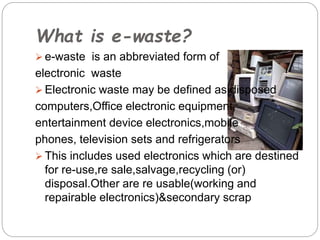
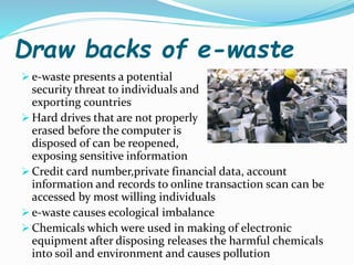
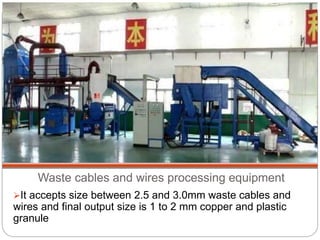
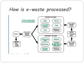
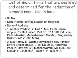
Regency Institute Of Technology
ELECTRONICS AND COMMUNICATON
ENGINEERING
SUBMITTED BY:
CONTENTS
What is e-waste?
Draw backs of e-waste
Need for e-waste processing
Equipment of e-waste processing
How is e-waste processed?
Difficulties involved in e-waste processing
Benefits of e-waste processing
Draw backs of e-waste processing
What is e-waste?
 e-waste is an abbreviated form of
electronic waste
 Electronic waste may be defined as disposed
computers,Office electronic equipment,
entertainment device electronics,mobile
phones, television sets and refrigerators
 This includes used electronics which are destined
for re-use,re sale,salvage,recycling (or)
disposal.Other are re usable(working and
repairable electronics)&secondary scrap
Draw backs of e-waste
 e-waste presents a potential
security threat to individuals and
exporting countries
 Hard drives that are not properly
erased before the computer is
disposed of can be reopened,
exposing sensitive information
 Credit card number,private financial data, account
information and records to online transaction scan can be
accessed by most willing individuals
 e-waste causes ecological imbalance
 Chemicals which were used in making of electronic
equipment after disposing releases the harmful chemicals
into soil and environment and causes pollution
Need for e-waste processing
 In order to reduce the e-waste pollution processing
of e-waste must be done accordingly
 Due to over pollution caused by these e-wastes the
governments of each and every country declared
special environmental and e-waste processing acts
in order to reduce the e-waste
 This has raised the need and deed for the e-waste
processing
 Due to continuous disposal of metals used in the
manufacturing of electronic waste one or the other
day metals may become extinct. So there is a need
for e-waste processing
Equipment required
for e-waste
processing
Cathode ray seperation and recycling equipment
It processes the cathode ray tube in the disposed waste of the computers
Printed circuit board(PCB processing equipment)
It is used in processing of printed circuit boards from
which the metals such as copper and aluminium are
extracted
Waste cables and wires processing equipment
It accepts size between 2.5 and 3.0mm waste cables and
wires and final output size is 1 to 2 mm copper and plastic
granule
How is e-waste processed?
In many developed countries electronic waste processing first
involves dismantling the equipment into various parts such as
metal frames,power supplies,circuit boards,palstic often by
hand
But due to rise in demand of e-waste processed products the
processes are done by shredding equipment
A typical example is the ‘NADIN’ electronic work processing
plant is NOVILSKAR,BULGARIA,the largest facility of its kind
in eastern Europe
Advantages of this process are the human ability to recognise
and save working and repairable parts such as chips,RAM’s etc
A hopper conveys material for shredding into an un
sophisticated mechanical separator with screening and
gramilating machines to separate constituent metal and
plastic fractions such regulating machinery is enclosed and
employs a dust collection system
 Some of the emissions are caught by scrubbers and
screens,magnets,eddy currents and tromel screens
employed to separate glass,palstic,ferrous and non ferrous
metals which can then be separated at smelter
 Leaded glass from CRT is used in car batteries,ammunition
and lead wheel weights are sold to foundries as a fluxing
agent in processing raw lead ore
 Cu,Au,Pd,Ag,Sn are valuable metals sold to smelter for re
cycling
 An ideal electronic waste processing plant combines
dismantling for component recovery with increase cost
effective processing of bulk electronic waste
 Devices still need eventual processing but by allowing other
Difficulties involved in e-waste
processing
 One of the major challenges is recycling the
printed circuit boards from electronic wastes
 The circuit boards contain precious metals such
as gold,silver,platinum,etc..and other base metals
such as copper,aluminium and iron
 One way e-waste is processed by melting circuit
boards,burning cable sheathing to recover copper
wire and open pit acid leading to separating
metals of value
 Initial cost for establishing e-waste processing
plant is high
 Skilled labour are required to operate the plant
benefits of e-waste
processing
 Most electronics devices contain a variety of
materials,including metals that can be recovered for
future uses
 By dismantling and providing reuse possibilities intact
natural resources are conserved and air and water
pollution caused by hazardous disposal is avoided
 Additionally processing of e-waste reduces the
amount of green house gases emissions caused by
manufacturing of new products
 The new products which are processed from these
industries can be used in the form of manufactured
goods which reduces the capital investment of
concerned industries
Draw backs of e-waste
processing
 e-waste processing has direct and indirect effects on
human health conditions
 Direct impact on human health may be caused by
dust in indoor air generated in manual and
mechanical dismantling processes.
ex:when processing plastics (or)CRT(cathode ray
tubes)
 Filter dust generated in mechanical dismantling
processes
 Noise emission during mechanical and manual
dismantling processes(conveyer belt and
hammering)
 Deviations from occupational safety standards
Conclusion
 At last, we conclude that today every one has to
realise the importance of e-waste processing and
government should provide encouragement for
firms which were especially established for this
purpose
 Mankind is responsible for the invention and for
the disposal of the electronic waste, so the
responsibility for processing the electronic waste
also depends on the mankind
List of indian firms that are destined
and determined for the reduction of
e-waste reduction in india
 Sl. No
 State Number of Registration on Recycler
 Name & Address
 1. Andhra Pradesh 2 Unit 1. M/s. Earth Sense
recycle Private Limited, Plot No. 37,APIIC Industrial
Park, Mankhal, Maheshwaram Mandal, Rangareddy
District - AP (1,800 MTA)
 2. M/s Ramky E- Waste Recycling Facility (Ramky
Enviro Engineers Ltd) , Plot No. 25 A, Hardware
Park, K. Raviryal (V), Maheshwaram (M), R.R. Dist -
500081 (10,000 MTA) Total = 11, 800 MTA
THANK YOU
Any Queries

E waste processing

  • 1.
    Regency Institute OfTechnology ELECTRONICS AND COMMUNICATON ENGINEERING SUBMITTED BY:
  • 2.
    CONTENTS What is e-waste? Drawbacks of e-waste Need for e-waste processing Equipment of e-waste processing How is e-waste processed? Difficulties involved in e-waste processing Benefits of e-waste processing Draw backs of e-waste processing
  • 3.
    What is e-waste? e-waste is an abbreviated form of electronic waste  Electronic waste may be defined as disposed computers,Office electronic equipment, entertainment device electronics,mobile phones, television sets and refrigerators  This includes used electronics which are destined for re-use,re sale,salvage,recycling (or) disposal.Other are re usable(working and repairable electronics)&secondary scrap
  • 4.
    Draw backs ofe-waste  e-waste presents a potential security threat to individuals and exporting countries  Hard drives that are not properly erased before the computer is disposed of can be reopened, exposing sensitive information  Credit card number,private financial data, account information and records to online transaction scan can be accessed by most willing individuals  e-waste causes ecological imbalance  Chemicals which were used in making of electronic equipment after disposing releases the harmful chemicals into soil and environment and causes pollution
  • 5.
    Need for e-wasteprocessing  In order to reduce the e-waste pollution processing of e-waste must be done accordingly  Due to over pollution caused by these e-wastes the governments of each and every country declared special environmental and e-waste processing acts in order to reduce the e-waste  This has raised the need and deed for the e-waste processing  Due to continuous disposal of metals used in the manufacturing of electronic waste one or the other day metals may become extinct. So there is a need for e-waste processing
  • 6.
    Equipment required for e-waste processing Cathoderay seperation and recycling equipment It processes the cathode ray tube in the disposed waste of the computers
  • 7.
    Printed circuit board(PCBprocessing equipment) It is used in processing of printed circuit boards from which the metals such as copper and aluminium are extracted
  • 8.
    Waste cables andwires processing equipment It accepts size between 2.5 and 3.0mm waste cables and wires and final output size is 1 to 2 mm copper and plastic granule
  • 9.
    How is e-wasteprocessed?
  • 10.
    In many developedcountries electronic waste processing first involves dismantling the equipment into various parts such as metal frames,power supplies,circuit boards,palstic often by hand But due to rise in demand of e-waste processed products the processes are done by shredding equipment A typical example is the ‘NADIN’ electronic work processing plant is NOVILSKAR,BULGARIA,the largest facility of its kind in eastern Europe Advantages of this process are the human ability to recognise and save working and repairable parts such as chips,RAM’s etc
  • 11.
    A hopper conveysmaterial for shredding into an un sophisticated mechanical separator with screening and gramilating machines to separate constituent metal and plastic fractions such regulating machinery is enclosed and employs a dust collection system  Some of the emissions are caught by scrubbers and screens,magnets,eddy currents and tromel screens employed to separate glass,palstic,ferrous and non ferrous metals which can then be separated at smelter  Leaded glass from CRT is used in car batteries,ammunition and lead wheel weights are sold to foundries as a fluxing agent in processing raw lead ore  Cu,Au,Pd,Ag,Sn are valuable metals sold to smelter for re cycling  An ideal electronic waste processing plant combines dismantling for component recovery with increase cost effective processing of bulk electronic waste  Devices still need eventual processing but by allowing other
  • 12.
    Difficulties involved ine-waste processing  One of the major challenges is recycling the printed circuit boards from electronic wastes  The circuit boards contain precious metals such as gold,silver,platinum,etc..and other base metals such as copper,aluminium and iron  One way e-waste is processed by melting circuit boards,burning cable sheathing to recover copper wire and open pit acid leading to separating metals of value  Initial cost for establishing e-waste processing plant is high  Skilled labour are required to operate the plant
  • 13.
    benefits of e-waste processing Most electronics devices contain a variety of materials,including metals that can be recovered for future uses  By dismantling and providing reuse possibilities intact natural resources are conserved and air and water pollution caused by hazardous disposal is avoided  Additionally processing of e-waste reduces the amount of green house gases emissions caused by manufacturing of new products  The new products which are processed from these industries can be used in the form of manufactured goods which reduces the capital investment of concerned industries
  • 14.
    Draw backs ofe-waste processing  e-waste processing has direct and indirect effects on human health conditions  Direct impact on human health may be caused by dust in indoor air generated in manual and mechanical dismantling processes. ex:when processing plastics (or)CRT(cathode ray tubes)  Filter dust generated in mechanical dismantling processes  Noise emission during mechanical and manual dismantling processes(conveyer belt and hammering)  Deviations from occupational safety standards
  • 15.
    Conclusion  At last,we conclude that today every one has to realise the importance of e-waste processing and government should provide encouragement for firms which were especially established for this purpose  Mankind is responsible for the invention and for the disposal of the electronic waste, so the responsibility for processing the electronic waste also depends on the mankind
  • 16.
    List of indianfirms that are destined and determined for the reduction of e-waste reduction in india  Sl. No  State Number of Registration on Recycler  Name & Address  1. Andhra Pradesh 2 Unit 1. M/s. Earth Sense recycle Private Limited, Plot No. 37,APIIC Industrial Park, Mankhal, Maheshwaram Mandal, Rangareddy District - AP (1,800 MTA)  2. M/s Ramky E- Waste Recycling Facility (Ramky Enviro Engineers Ltd) , Plot No. 25 A, Hardware Park, K. Raviryal (V), Maheshwaram (M), R.R. Dist - 500081 (10,000 MTA) Total = 11, 800 MTA
  • 17.
  • 18.