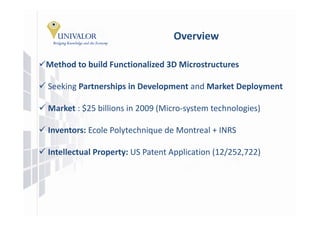
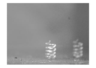
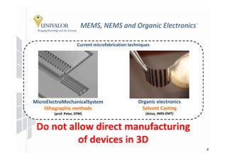
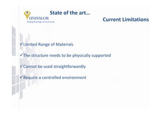
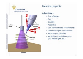
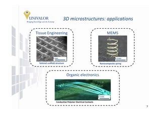
Direct 3D 
       Di     3D
Microfabrication Process


Presented by Thomas Martinuzzo
Project Manager, Sciences and Engineering
thomas.martinuzzo@univalor.ca
Overview

Method b ild Functionalized 3D Mi
M h d to build F  i   li d 3D Microstructures

Seeking Partnerships in Development and Market Deployment
                     in Development

Market : $25 billions in 2009 (Micro‐system technologies)

Inventors: Ecole Polytechnique de Montreal + INRS

Intellectual Property: US Patent Application (12/252,722)
MEMS, NEMS and Organic Electronics
                         MEMS NEMS and Organic Electronics

                      Current microfabrication t h i
                      C     t i f b i ti techniques


MicroElectroMechanicalSystem                   Organic electronics 
    lithographic methods                        Solvent Casting
        (prof. Peter, EPM)                        (Aissa, INRS‐EMT)


 Do not allow direct manufacturing 
          of devices in 3D
                                                                      4
State of the art…
                                         Current Limitations
                                         C     t Li it ti


Limited Range of Materials
Limited Range of Materials

The structure needs to be physically supported
                          p y      y pp

Cannot be used straightforwardly

Require a controlled environment
Technical aspects 

                                            Advantages:
                                               –   Cost‐effective
                                                   Cost effective
                                               –   Fast
                                               –   Scalable
Radiation                     Dispensing       –   Repetitive
source                        apparatus
                                               –   Low environmental requirements
                                               –   Direct writing of 3D structures
                                               –   Variability of materials 
                                               –   Variability of radiation source 
                                                   Variability of radiation source
                         Extruded 
                         material                  (UV, Visible light, etc.)


             Schematic

                                                                                      6
3D microstructures: applications
                          3D microstructures: applications

Tissue Engineering                                                   MEMS


                1 mm                                                       2.5 mm

 Tailored scaffold structure                                 Nanocomposite spring


                               Organic electronics


                                                            2.5 mm

                   Conductive Polymer Electrical Contacts

                                                                                    7
Target Markets
                       Target Markets

• Ti
  Tissue Engineering
         E i     i
  – $15 billion now
    $
• MEMS
  – $12.5 billion in 2010
• Organic Electronics
  Organic Electronics
  – $25 billion in 2015
  – $250 billions in 2025

                                        8
Team
Louis Laberge Lebel, Ph.D
Louis Laberge Lebel Ph D Student
 • Ecole Polytechnique de Montreal
Pr. Daniel Terriault, Ph.D
 • Professor
Pr. My Ali El Khakani, Ph.D
 • Professor INRS
Brahim Aissa, Ph.D Student
 • INRS
                                     INRS-EMT
Summary

Simple Idea
Si l Id

Developed Within Academic Institution

Through Boostrapping Financing
     g         pp g          g

Core IP

Various Market Segments

 Looking For Partnerships in Development and Market
                      Deployment
                         p y
Direct 3D Microfabrication Process

     Thomas Martinuzzo
thomas.martinuzzo@univalor.ca
thomas martinuzzo@univalor ca

Direct Writing

  • 1.
    Direct 3D  Di 3D Microfabrication Process Presented by Thomas Martinuzzo Project Manager, Sciences and Engineering thomas.martinuzzo@univalor.ca
  • 2.
    Overview Method b ildFunctionalized 3D Mi M h d to build F i li d 3D Microstructures Seeking Partnerships in Development and Market Deployment in Development Market : $25 billions in 2009 (Micro‐system technologies) Inventors: Ecole Polytechnique de Montreal + INRS Intellectual Property: US Patent Application (12/252,722)
  • 4.
    MEMS, NEMS and Organic Electronics MEMS NEMS and Organic Electronics Current microfabrication t h i C t i f b i ti techniques MicroElectroMechanicalSystem Organic electronics  lithographic methods Solvent Casting (prof. Peter, EPM) (Aissa, INRS‐EMT) Do not allow direct manufacturing  of devices in 3D 4
  • 5.
    State of the art… Current Limitations C t Li it ti Limited Range of Materials Limited Range of Materials The structure needs to be physically supported p y y pp Cannot be used straightforwardly Require a controlled environment
  • 6.
    Technical aspects  Advantages: – Cost‐effective Cost effective – Fast – Scalable Radiation  Dispensing  – Repetitive source apparatus – Low environmental requirements – Direct writing of 3D structures – Variability of materials  – Variability of radiation source  Variability of radiation source Extruded  material (UV, Visible light, etc.) Schematic 6
  • 7.
    3D microstructures: applications 3D microstructures: applications Tissue Engineering MEMS 1 mm 2.5 mm Tailored scaffold structure Nanocomposite spring Organic electronics 2.5 mm Conductive Polymer Electrical Contacts 7
  • 8.
    Target Markets Target Markets • Ti Tissue Engineering E i i – $15 billion now $ • MEMS – $12.5 billion in 2010 • Organic Electronics Organic Electronics – $25 billion in 2015 – $250 billions in 2025 8
  • 9.
    Team Louis Laberge Lebel, Ph.D Louis Laberge LebelPh D Student • Ecole Polytechnique de Montreal Pr. Daniel Terriault, Ph.D • Professor Pr. My Ali El Khakani, Ph.D • Professor INRS Brahim Aissa, Ph.D Student • INRS INRS-EMT
  • 10.
    Summary Simple Idea Si l Id DevelopedWithin Academic Institution Through Boostrapping Financing g pp g g Core IP Various Market Segments Looking For Partnerships in Development and Market Deployment p y
  • 11.
    Direct 3D Microfabrication Process Thomas Martinuzzo thomas.martinuzzo@univalor.ca thomas martinuzzo@univalor ca