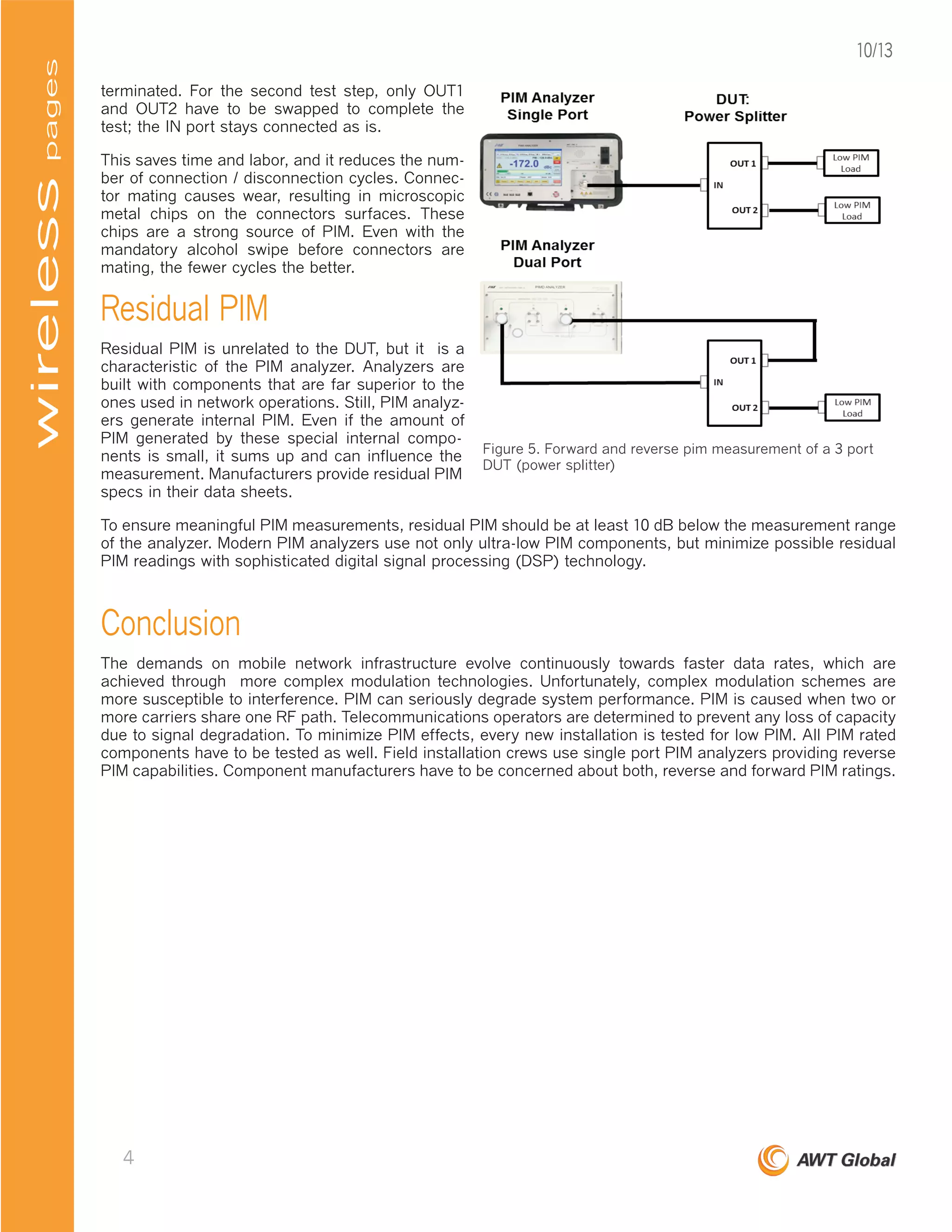
Passive Intermodulation (PIM) distortion is a growing concern for telecommunication network operators. They have to cope with limited bandwidths and at the same time, with highest data demand of their subscribers. Learn more about PIM, its causes and measuring.
LOW POWER SI CLASS E POWER AMPLIFIER AND RF SWITCH FOR HEALTH CAREieijjournal
This research was to design a 2.4 GHz class E Power Amplifier (PA) for health care, with 0.18um
Semiconductor Manufacturing International Corporation CMOS technology by using Cadence software.
And also RF switch was designed at cadence software with power Jazz 180nm SOI process. The ultimate
goal for such application is to reach high performance and low cost, and between high performance and
low power consumption design. This paper introduces the design of a 2.4GHz class E power amplifier and RF switch design. PA consists of cascade stage with negative capacitance. This power amplifier can transmit 16dBm output power to a 50Ω load. The performance of the power amplifier and switch meet the specification requirements of the desired.
DESIGN OF DIGITAL PLL USING OPTIMIZED PHASE NOISE VCOVLSICS Design
In order to keep electronic world properly PLL plays a very important role. Designing of low
phase noise and less jittery PLL in generation of clock signals is an important task. Clock signals
are required for providing reference timing to electrical system and also to ICs. So in this paper
PLL is designed with improved Phase noise and also jitter. Where such types of design is
important when sophisticated timing requirements are needed to provide synchronization and
distribution of clocks like in ADC, DAC, high speed networking, medical imaging systems. The
clock signal’s quality depends upon jitter and phase noise. An ideal clock source has zero phase
noise and jitter but in reality it has some modulated phase noise. This modulated phase noise
spreads the power to the adjacent frequencies, hence produces noise sidebands. The phase noise
is typically frequency domain analysis which is expressed in terms of dBc/Hz measured at offset
frequency with respect to ideal clock frequency. The low phase noise is important factor mainly
in RF and ADC applications. In RF wireless high speed applications, increased PN will leads to
channel to channel interference, attenuates quality of signal. In ADC, increased PN limits the
SNR and data converter’s equivalent no. of bits (ENOB). Jitter is time domain meas
Cdma2000 network problem analysis with mobile station 20030212-a-v1.0Tempus Telcosys
Keyword: CDMA, forward coverage, reverse coverage and connection
Abstract: This document describes how to use a Mobile Station (MS) to locate network problems. That is, judge the forward/reverse coverage by viewing the indices displayed on the Debug screen of MS. Then locate the network problems according to reverse Frame Error Rate (FER) and Received Signal Strength Indicator (RSSI) test on the background. This document uses H100 MS as an example for the description. For settings of other CDMA MSs, see the relevant document.
1.1
Displaying Debug Screen of H100 MS
1.2
1) 2) 3) 4)
Switch on the MS; Input password: ##27732726; Press the red Power-off key; Select 3.
The Debug screen is displayed.
Index Value on Debug Screen
Assume that the following information is displayed on the Debug screen:
P232 R085 C0210
03612-00001-1
PAGE Ec: -5.0
RX: -75 TX: NoTx
P232: PN of primary service sector
C0210: System operating frequency
03612: SID
00001: NID
PAGE: Channel mode
Ec: Ec/Io
Rx: Receive level of MS
TX: Transmit level of MS
Thou
Design and Simulation of First Order Sigma-Delta Modulator Using LT spice ToolIJERA Editor
A switched-capacitor single-stage Sigma-Delta ADC with a first-order modulator is proposed. Efficient low power first Order 1-Bit Sigma-Delta ADC designed which accepts input signal bandwidth of 10 MHz. This circuitry performs the function of an analog-to-digital converter. A first-order 1-Bit Sigma-Delta (Σ-Δ) modulator is designed, simulated and analyzed using LTspice standard 250nm CMOS technology power supply of 1.8V. The modulator is proved to be robustness, the high performance in stability. The simulations are compared with those from a traditional analog-to-digital converter to prove that Sigma-Delta is performing better with low power and area.
LOW POWER SI CLASS E POWER AMPLIFIER AND RF SWITCH FOR HEALTH CAREieijjournal1
This research was to design a 2.4 GHz class E Power Amplifier (PA) for health care, with 0.18um
Semiconductor Manufacturing International Corporation CMOS technology by using Cadence software.
And also RF switch was designed at cadence software with power Jazz 180nm SOI process. The ultimate
goal for such application is to reach high performance and low cost, and between high performance and
low power consumption design. This paper introduces the design of a 2.4GHz class E power amplifier and
RF switch design. PA consists of cascade stage with negative capacitance. This power amplifier can
transmit 16dBm output power to a 50Ω load. The performance of the power amplifier and switch meet the
specification requirements of the desired.
LOW POWER SI CLASS E POWER AMPLIFIER AND RF SWITCH FOR HEALTH CAREieijjournal
This research was to design a 2.4 GHz class E Power Amplifier (PA) for health care, with 0.18um
Semiconductor Manufacturing International Corporation CMOS technology by using Cadence software.
And also RF switch was designed at cadence software with power Jazz 180nm SOI process. The ultimate goal for such application is to reach high performance and low cost, and between high performance and low power consumption design. This paper introduces the design of a 2.4GHz class E power amplifier and
RF switch design. PA consists of cascade stage with negative capacitance. This power amplifier can
transmit 16dBm output power to a 50Ω load. The performance of the power amplifier and switch meet the specification requirements of the desired.
LOW POWER SI CLASS E POWER AMPLIFIER AND RF SWITCH FOR HEALTH CAREieijjournal
This research was to design a 2.4 GHz class E Power Amplifier (PA) for health care, with 0.18um
Semiconductor Manufacturing International Corporation CMOS technology by using Cadence software.
And also RF switch was designed at cadence software with power Jazz 180nm SOI process. The ultimate
goal for such application is to reach high performance and low cost, and between high performance and
low power consumption design. This paper introduces the design of a 2.4GHz class E power amplifier and
RF switch design. PA consists of cascade stage with negative capacitance. This power amplifier can
transmit 16dBm output power to a 50Ω load. The performance of the power amplifier and switch meet the
specification requirements of the desired
Low Power SI Class E Power Amplifier and Rf Switch for Health Careieijjournal1
This research was to design a 2.4 GHz class E Power Amplifier (PA) for health care, with 0.18um Semiconductor Manufacturing International Corporation CMOS technology by using Cadence software. And also RF switch was designed at cadence software with power Jazz 180nm SOI process. The ultimate goal for such application is to reach high performance and low cost, and between high performance and low power consumption design. This paper introduces the design of a 2.4GHz class E power amplifier and RF switch design. PA consists of cascade stage with negative capacitance. This power amplifier can transmit 16dBm output power to a 50Ω load. The performance of the power amplifier and switch meet the specification requirements of the desired.
This presentation reviews the different methods of communicating to your meters, the reasons for them, and some of the testing and challenges related to them.
Review on Design and Performance Analysis of Low Power Transceiver Circuit in...iosrjce
IOSR Journal of Electronics and Communication Engineering(IOSR-JECE) is a double blind peer reviewed International Journal that provides rapid publication (within a month) of articles in all areas of electronics and communication engineering and its applications. The journal welcomes publications of high quality papers on theoretical developments and practical applications in electronics and communication engineering. Original research papers, state-of-the-art reviews, and high quality technical notes are invited for publications.
Observability Concepts EVERY Developer Should Know -- DeveloperWeek Europe.pdfPaige Cruz
Monitoring and observability aren’t traditionally found in software curriculums and many of us cobble this knowledge together from whatever vendor or ecosystem we were first introduced to and whatever is a part of your current company’s observability stack.
While the dev and ops silo continues to crumble….many organizations still relegate monitoring & observability as the purview of ops, infra and SRE teams. This is a mistake - achieving a highly observable system requires collaboration up and down the stack.
I, a former op, would like to extend an invitation to all application developers to join the observability party will share these foundational concepts to build on:
Smart TV Buyer Insights Survey 2024 by 91mobiles.pdf91mobiles
91mobiles recently conducted a Smart TV Buyer Insights Survey in which we asked over 3,000 respondents about the TV they own, aspects they look at on a new TV, and their TV buying preferences.
UiPath Test Automation using UiPath Test Suite series, part 4DianaGray10
Welcome to UiPath Test Automation using UiPath Test Suite series part 4. In this session, we will cover Test Manager overview along with SAP heatmap.
The UiPath Test Manager overview with SAP heatmap webinar offers a concise yet comprehensive exploration of the role of a Test Manager within SAP environments, coupled with the utilization of heatmaps for effective testing strategies.
Participants will gain insights into the responsibilities, challenges, and best practices associated with test management in SAP projects. Additionally, the webinar delves into the significance of heatmaps as a visual aid for identifying testing priorities, areas of risk, and resource allocation within SAP landscapes. Through this session, attendees can expect to enhance their understanding of test management principles while learning practical approaches to optimize testing processes in SAP environments using heatmap visualization techniques
What will you get from this session?
1. Insights into SAP testing best practices
2. Heatmap utilization for testing
3. Optimization of testing processes
4. Demo
Topics covered:
Execution from the test manager
Orchestrator execution result
Defect reporting
SAP heatmap example with demo
Speaker:
Deepak Rai, Automation Practice Lead, Boundaryless Group and UiPath MVP
Essentials of Automations: Optimizing FME Workflows with ParametersSafe Software
Are you looking to streamline your workflows and boost your projects’ efficiency? Do you find yourself searching for ways to add flexibility and control over your FME workflows? If so, you’re in the right place.
Join us for an insightful dive into the world of FME parameters, a critical element in optimizing workflow efficiency. This webinar marks the beginning of our three-part “Essentials of Automation” series. This first webinar is designed to equip you with the knowledge and skills to utilize parameters effectively: enhancing the flexibility, maintainability, and user control of your FME projects.
Here’s what you’ll gain:
- Essentials of FME Parameters: Understand the pivotal role of parameters, including Reader/Writer, Transformer, User, and FME Flow categories. Discover how they are the key to unlocking automation and optimization within your workflows.
- Practical Applications in FME Form: Delve into key user parameter types including choice, connections, and file URLs. Allow users to control how a workflow runs, making your workflows more reusable. Learn to import values and deliver the best user experience for your workflows while enhancing accuracy.
- Optimization Strategies in FME Flow: Explore the creation and strategic deployment of parameters in FME Flow, including the use of deployment and geometry parameters, to maximize workflow efficiency.
- Pro Tips for Success: Gain insights on parameterizing connections and leveraging new features like Conditional Visibility for clarity and simplicity.
We’ll wrap up with a glimpse into future webinars, followed by a Q&A session to address your specific questions surrounding this topic.
Don’t miss this opportunity to elevate your FME expertise and drive your projects to new heights of efficiency.
State of ICS and IoT Cyber Threat Landscape Report 2024 previewPrayukth K V
The IoT and OT threat landscape report has been prepared by the Threat Research Team at Sectrio using data from Sectrio, cyber threat intelligence farming facilities spread across over 85 cities around the world. In addition, Sectrio also runs AI-based advanced threat and payload engagement facilities that serve as sinks to attract and engage sophisticated threat actors, and newer malware including new variants and latent threats that are at an earlier stage of development.
The latest edition of the OT/ICS and IoT security Threat Landscape Report 2024 also covers:
State of global ICS asset and network exposure
Sectoral targets and attacks as well as the cost of ransom
Global APT activity, AI usage, actor and tactic profiles, and implications
Rise in volumes of AI-powered cyberattacks
Major cyber events in 2024
Malware and malicious payload trends
Cyberattack types and targets
Vulnerability exploit attempts on CVEs
Attacks on counties – USA
Expansion of bot farms – how, where, and why
In-depth analysis of the cyber threat landscape across North America, South America, Europe, APAC, and the Middle East
Why are attacks on smart factories rising?
Cyber risk predictions
Axis of attacks – Europe
Systemic attacks in the Middle East
Download the full report from here:
https://sectrio.com/resources/ot-threat-landscape-reports/sectrio-releases-ot-ics-and-iot-security-threat-landscape-report-2024/
LF Energy Webinar: Electrical Grid Modelling and Simulation Through PowSyBl -...DanBrown980551
Do you want to learn how to model and simulate an electrical network from scratch in under an hour?
Then welcome to this PowSyBl workshop, hosted by Rte, the French Transmission System Operator (TSO)!
During the webinar, you will discover the PowSyBl ecosystem as well as handle and study an electrical network through an interactive Python notebook.
PowSyBl is an open source project hosted by LF Energy, which offers a comprehensive set of features for electrical grid modelling and simulation. Among other advanced features, PowSyBl provides:
- A fully editable and extendable library for grid component modelling;
- Visualization tools to display your network;
- Grid simulation tools, such as power flows, security analyses (with or without remedial actions) and sensitivity analyses;
The framework is mostly written in Java, with a Python binding so that Python developers can access PowSyBl functionalities as well.
What you will learn during the webinar:
- For beginners: discover PowSyBl's functionalities through a quick general presentation and the notebook, without needing any expert coding skills;
- For advanced developers: master the skills to efficiently apply PowSyBl functionalities to your real-world scenarios.
Elevating Tactical DDD Patterns Through Object CalisthenicsDorra BARTAGUIZ
After immersing yourself in the blue book and its red counterpart, attending DDD-focused conferences, and applying tactical patterns, you're left with a crucial question: How do I ensure my design is effective? Tactical patterns within Domain-Driven Design (DDD) serve as guiding principles for creating clear and manageable domain models. However, achieving success with these patterns requires additional guidance. Interestingly, we've observed that a set of constraints initially designed for training purposes remarkably aligns with effective pattern implementation, offering a more ‘mechanical’ approach. Let's explore together how Object Calisthenics can elevate the design of your tactical DDD patterns, offering concrete help for those venturing into DDD for the first time!
A tale of scale & speed: How the US Navy is enabling software delivery from l...sonjaschweigert1
Rapid and secure feature delivery is a goal across every application team and every branch of the DoD. The Navy’s DevSecOps platform, Party Barge, has achieved:
- Reduction in onboarding time from 5 weeks to 1 day
- Improved developer experience and productivity through actionable findings and reduction of false positives
- Maintenance of superior security standards and inherent policy enforcement with Authorization to Operate (ATO)
Development teams can ship efficiently and ensure applications are cyber ready for Navy Authorizing Officials (AOs). In this webinar, Sigma Defense and Anchore will give attendees a look behind the scenes and demo secure pipeline automation and security artifacts that speed up application ATO and time to production.
We will cover:
- How to remove silos in DevSecOps
- How to build efficient development pipeline roles and component templates
- How to deliver security artifacts that matter for ATO’s (SBOMs, vulnerability reports, and policy evidence)
- How to streamline operations with automated policy checks on container images
Builder.ai Founder Sachin Dev Duggal's Strategic Approach to Create an Innova...Ramesh Iyer
In today's fast-changing business world, Companies that adapt and embrace new ideas often need help to keep up with the competition. However, fostering a culture of innovation takes much work. It takes vision, leadership and willingness to take risks in the right proportion. Sachin Dev Duggal, co-founder of Builder.ai, has perfected the art of this balance, creating a company culture where creativity and growth are nurtured at each stage.
Builder.ai Founder Sachin Dev Duggal's Strategic Approach to Create an Innova...
About PIM: Forward - Reverse - Residual
1. wireless
About PIM: Forward - Reverse - Residual
P
assive intermodulation
(PIM) distortion is a grow-
ing concern for telecommu-
nication network operators.
They have to cope with limited band-
widths and at the same time, with
highest data demand of their sub-
scribers. Signal degradation caused
by PIM reduces available bandwidth
and can seriously impair mobile net-
work quality. PIM analyzers play an
important role in tackling the PIM
problem, in the field but also in de-
velopment labs.
PIM is an unwanted signal distortion
caused by non-linear behavior of
passive components in the RF path
of telecommunication systems. PIM happens when these systems carry two or more RF signals simul-
taneously. Multi carrier systems are the norm with today's in-building DAS installations. Not only can
PIM degrade signal quality, it can affect system performance so severely that it may even drop calls.
Users become disgruntled about poor service, network operators lose revenue.
Modern telecommunication networks are challenged as never before with subscribers demanding
huge data volumes for smart phones and tablets. To maintain the highest levels of network cover-
age, performance and reliability, all sources of interference that might affect signal quality need to be
eliminated.
PIM can be caused by a number of sources, including:
„„ Junctions of dissimilar metals with different electrical properties
„„ Corroded components and structures
„„ Ferromagnetic metals like iron, nickel and steel
„„ Irregular contact areas, even on microscopic scale, that cause an inconsistent flow of elec-
trons and generate inhomogeneous electrical fields
„„ Spark discharges caused by "hot" connections and disconnections, producing craters on
connector surfaces and leading to chemical reactions.
„„ Rusty-Bolt- effects. This is PIM caused in the RF path between transmitter antenna and
receiver antenna.
The need to minimize PIM effects makes testing for passive intermodulation (PIM) in components and
cellular installations a mandatory task. This is especially important for systems that share more than
one carrier, as it is the case with neutral-host distributed antenna systems (DAS).
wireless
AWTGlobal
117GrandAvenue,Hackettstown,NJ07840,USA
w:www.awt-global.com|e:info@awt-global.com|p:+1973--321-3423
10/13
by Wolfgang Damm | AWT Global
pages
An AWT Global Publication
2. 2
Forward & Reverse PIM
If PIM levels of telecommunication installation are
too high, culprits are often found in components
and connections. Dust or metal chips in the con-
nector areas, scratched plating surfaces or dis-
similar metals can induce PIM. Figure 1a shows a
connection between two feeder cables. If the con-
nection is causing PIM, it can be seen like the elec-
trical model in Figure 1b. The RF source represents
the PIM source in the connectors, generating low
power signals at a frequency that correlates to the
intermodulation signal. The generator injects the IM
signal into the feeder cables in a way that it propa-
gates in both directions: towards the system's output
(antenna) and towards the systems input (receiver).
PIM in the direction of the antenna is called for-
ward PIM. Intermodulation power that is propagating
towards the receiver is known as reflected or reverse
PIM. The receiver of the base station is replaced by
the receiver of the PIM analyzer during PIM tests.
Incoming receiver signals are naturally very weak, and can go as low as -117 dBm. It does not take a lot of
energy to interfere with these signals. If reverse PIM interferes with these incoming up-link signals, receivers
get seriously distorted and the quality of wireless connections drops significantly.
Measuring PIM
Many passive RF components, like attenuators, can
be utilized in both directions. Forward and reverse PIM
measurements of components may display slightly
different results. Therefore, PIM ratings on manufac-
turers' data sheets should include both forward and
reverse PIM characteristics.
International standard for PIM measurements is IEC
62037. Only PIM testers fully conform to this stan-
dard guarantee that measurements are conducted in
a meaningful, comparable and repeatable manner.
PIM analyzers are vital tools for both, R&D engineers
and field installation crews. Analyzers used by field
personal are typically single port systems, while dual
port analyzers are used at production floors. Dual port
analyzers are not to be confused with dual band PIM
analyzers. What is the difference? The latter have the
capability to measure two different frequency bands;
the former provide two ports, one to perform reverse
PIM measurements, the other for forward PM mea-
surements.
Single- and dual port PIM analyzers share the larger part of their architecture (Figure 2). Both incorporate two
variable, independent RF generators which drive two high-power amplifiers (HPAs). The generated signals are
variable in frequency and level. The generators can be set to any frequency in the specific band for which the
PIM analyzer has been designed. An ultra low PIM combiner brings the amplified signals together and delivers
the combined carriers to the Tx port of a duplexer. The duplexer has to provide very high separation between its
pageswireless
Figure 1. Electrical model of PIM source in RF system.
Figure 2. Block diagram of single port and dual port PIM
analyzers.
10/13
3. high power Tx and very low power Rx ports. As better this duplexer is designed, as better the dynamic range of
the PIM test system. The output of the duplexer is basically the reverse PIM port of the PIM analyzer. With the
exception of antennas and loads, all Devices Under Test (DUTs) require external terminations to perform PIM
measurements. Antennas radiate the transmitted RF power
directly into the air, loads convert it into heat. Any test cable
and load that is used for PIM testing, must have significantly
better PIM ratings than the actual DUT to allow for accurate
measurements.
PIM signals that arrive at the analyzer port are channeled to
the duplexer's Rx leg. The duplexer frequency correlates with
the receiving band of the wireless system. A highly selective
receiver measures now the power of the intermodulation sig-
nal.
Dual-port analyzers consists of all these elements, but have
a second duplexer (identical to the first), an additional inter-
nal high power, low PIM termination and a low PIM switch.
The second port feeds into the second duplexer, which has a
terminated Tx port. Since an internal termination is provided,
dual-port analyzers do not require external loads to terminate
2-port DUTs. The Rx port of the second duplexer measures
forward PIM power. A low PIM switch toggles between reverse
and forward PIM measurements.
Field technicians use single-port analyzers like the one shown
in Figure 3. During PIM measurements, system PAs and re-
ceivers of the RF systems are disconnected and instead PIM
analyzer are connected. The analyzers will now generate two
high-power CW tones within the transmit band of the measured system. It is important to apply enough energy
during PIM measurements to ensure the RF system is tested under conditions similar to the actual utilization.
Only measurements conducted with 2x20W systems apply realistic thermal load to connectors, allowing pin-
pointing (future) PIM issues.
Single or Dual Port Analyzers?
For many measurement applications in telecom-
munications, single-port analyzers are suitable for
both, reverse and forward PIM analysis. Figure 4
shows forward and reverse PIM measurements for
a simple two-terminal DUT; a cable in this exam-
ple. Forward and reverse PIM will not differ much,
and can easily be measured in two steps. Reverse
PIM is measured by connecting one end of the
DUT (A) to the PIM analyzer, while the other end
is terminated with a low PIM load (B). Forward PIM
is measured with the direction of the DUT reversed
(B-A). The resulting PIM measurements are quite
similar.
Dual-port units help measure forward and reverse PIM of components in less time. This is very beneficial for
complex components with more than two ports. The example in Figure 5 shows a power splitter under test.
Single-port units require three test steps, feeding the analyzer's measurement signals sequentially into the
splitter ports IN, OUT1 and OUT2. Ports that are not connected to the PIM analyzer need to be terminated for
accurate measurements. Dual port analyzers offer more convenient testing. During the first test step, mea-
surement signals are fed into IN port of the splitter, while the forward port is connected to OUT1, with OUT2
Figure 3. Portable PIM analyzer with constant
2x20 W output power, conform to PIM specifica-
tion IEC 62037.
Figure 4. Forward and reverse PIM measurement of cable,
as simple dual-port DUT (cable).
pageswireless
3
10/13
4. terminated. For the second test step, only OUT1
and OUT2 have to be swapped to complete the
test; the IN port stays connected as is.
This saves time and labor, and it reduces the num-
ber of connection / disconnection cycles. Connec-
tor mating causes wear, resulting in microscopic
metal chips on the connectors surfaces. These
chips are a strong source of PIM. Even with the
mandatory alcohol swipe before connectors are
mating, the fewer cycles the better.
Residual PIM
Residual PIM is unrelated to the DUT, but it is a
characteristic of the PIM analyzer. Analyzers are
built with components that are far superior to the
ones used in network operations. Still, PIM analyz-
ers generate internal PIM. Even if the amount of
PIM generated by these special internal compo-
nents is small, it sums up and can influence the
measurement. Manufacturers provide residual PIM
specs in their data sheets.
To ensure meaningful PIM measurements, residual PIM should be at least 10 dB below the measurement range
of the analyzer. Modern PIM analyzers use not only ultra-low PIM components, but minimize possible residual
PIM readings with sophisticated digital signal processing (DSP) technology.
Conclusion
The demands on mobile network infrastructure evolve continuously towards faster data rates, which are
achieved through more complex modulation technologies. Unfortunately, complex modulation schemes are
more susceptible to interference. PIM can seriously degrade system performance. PIM is caused when two or
more carriers share one RF path. Telecommunications operators are determined to prevent any loss of capacity
due to signal degradation. To minimize PIM effects, every new installation is tested for low PIM. All PIM rated
components have to be tested as well. Field installation crews use single port PIM analyzers providing reverse
PIM capabilities. Component manufacturers have to be concerned about both, reverse and forward PIM ratings.
Figure 5. Forward and reverse pim measurement of a 3 port
DUT (power splitter)
pageswireless
4
10/13