2
Testing Philosophy
Role ofTesting
Digital and Analog VLSI Testing
VLSI Technology Trends affecting Testing
Types of Testing
Defects, Errors and Faults
Functional Versus Structural Testing,
Levels of Fault Models
Single Stuck-at Fault
Contents
3.
3
If you area student now, or were in the past, you are quite familiar with the word test,
and probably hate it.
Understanding the teacher’s point of view will help.
The teacher sets a domain of knowledge for testing, called the course syllabus. It may be
the contents of a book, class notes, lectures, or some (arbitrary!) combination of all those.
Next, comes the testing method.
The teacher asks questions and analyzes the response, perhaps by matching answers to
correct ones from the book.
The quality of such a test system depends upon how well the test questions cover the
syllabus.
In VLSI testing also, one should know the specification (synonymous to the course
syllabus) of the object being tested and then devise tests such that if the object produces
the expected response then its conformance to the specification can be guaranteed.
Testing Philosophy
4.
4
Returning to ourstudent analogy, since no one has infinite time, the number
of questions must be limited, and they should be cleverly devised.
The teacher now makes certain assumptions.
Certain typical errors, ones that the student is likely to commit, are assumed.
Questions are devised especially to uncover those errors and, if the student’s
answers are correct, the teacher grants the benefit of doubt, showing
confidence in the implicit error model.
Electronic testing also uses fault modeling and tests are generated for the
assumed fault models.
In testing, successful experience with a fault model gives it credibility, and
eventually people expect reliability when a high percentage of the modeled
faults is tested.
Contd...
5.
5
Finally, remember that,if you fail, you must repeat the course. This
is similar to redesign and remake in our “Algorithm: Perfect.
” Of course, you can do better by asking your teacher, right at the
beginning, about
(1) the course syllabus and
(2) error models (i.e., what you will be tested for),
and then plan your studies to succeed.
In VLSI, that is called design for testability.
Contd...
6.
6
If you designa product, fabricate and test it, and it fails the test, then
there must be a cause for the failure.
Either (1) the test was wrong, or
(2) the fabrication process was faulty, or
(3) the design was incorrect, or
(4) the specification had a problem.
Anything can go wrong.
The role of testing is to detect whether something went wrong and the
role of diagnosis is to determine exactly what went wrong, and where the
process needs to be altered.
Therefore, correctness and effectiveness of testing is most important for
quality products (another name for perfect products.)
Role of Testing
7.
7
If the testprocedure is good and the product fails, then we suspect the
fabrication process, the design, or the specification.
If all students in a class fail then it is often considered the teacher’s
failure. If only some fail, we assume that the teacher is competent, but some
students are having difficulty.
To select students likely to succeed, teachers may use prerequisites or
admission tests for screening.
Distributed testing along a product realization process catches the
defect-producing causes as soon as they become active, and before they
have done much damage.
A well thought out test strategy is crucial to economical realization of
products.
Contd...
8.
8
The benefits oftesting are quality and economy.
These two attributes are not independent and neither can be defined
without the other.
Quality means satisfying the user’s needs at a minimum cost.
A good test process can weed out all bad products before they reach
the user.
However, if too many bad items are being produced then the cost of
those bad items will have to be recovered from the price charged for the
few good items that are produced.
It will be impossible for an engineer to de-sign a quality product
without a profound understanding of the physical principles underlying
the processes of manufacturing and test.
Contd...
9.
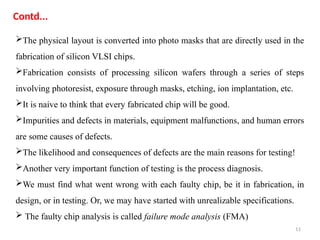
9
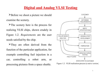
Before we shoota picture we should
examine the scenery.
The scenery here is the process for
realizing VLSI chips, shown crudely in
Figure 1.2. Requirements are the user
needs satisfied by the chip.
They are often derived from the
function of the particular application, for
example controlling fuel injection in a
car, controlling a robot arm, or
processing pictures from a space shuttle.
Digital and Analog VLSI Testing
Figure 1.2: VLSI realization process (a naive version.)
10.
10
One sets downthe specifications of various types, which include function
(input-output characteristics), operating characteristics (power, frequency,
noise, etc.), physical characteristics (packaging, etc.), environmental
characteristics (temperature, humidity, reliability, etc.), and other
characteristics (volume, cost, price, avail-ability, etc.)
The objective of design is to produce data necessary for the next steps of
fabrication and testing.
Design has several stages.
The first, known as architectural design, produces a system-level structure
of realizable blocks to implement the functional specification.
The second, called logic design, further decomposes blocks into logic
gates.
Finally, the gates are implemented as physical devices (e.g., transistors)
Contd...
11.
11
The physical layoutis converted into photo masks that are directly used in the
fabrication of silicon VLSI chips.
Fabrication consists of processing silicon wafers through a series of steps
involving photoresist, exposure through masks, etching, ion implantation, etc.
It is naive to think that every fabricated chip will be good.
Impurities and defects in materials, equipment malfunctions, and human errors
are some causes of defects.
The likelihood and consequences of defects are the main reasons for testing!
Another very important function of testing is the process diagnosis.
We must find what went wrong with each faulty chip, be it in fabrication, in
design, or in testing. Or, we may have started with unrealizable specifications.
The faulty chip analysis is called failure mode analysis (FMA)
Contd...
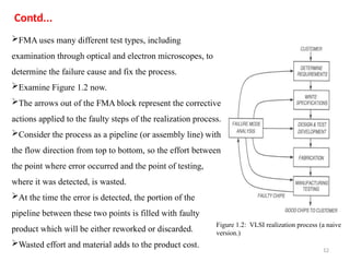
12.
12
FMA uses manydifferent test types, including
examination through optical and electron microscopes, to
determine the failure cause and fix the process.
Examine Figure 1.2 now.
The arrows out of the FMA block represent the corrective
actions applied to the faulty steps of the realization process.
Consider the process as a pipeline (or assembly line) with
the flow direction from top to bottom, so the effort between
the point where error occurred and the point of testing,
where it was detected, is wasted.
At the time the error is detected, the portion of the
pipeline between these two points is filled with faulty
product which will be either reworked or discarded.
Wasted effort and material adds to the product cost.
Figure 1.2: VLSI realization process (a naive
version.)
Contd...
13.
13
Testing should, therefore,be placed closest to the point of error.
Many companies emphasize on doing it right the first time, or pursuing the
goal of zero defects.
This does not mean that humans, or even machines, cannot make mistakes.
These goals are achievable in an error-prone environment, when errors are
detected and corrected before damage occurs.
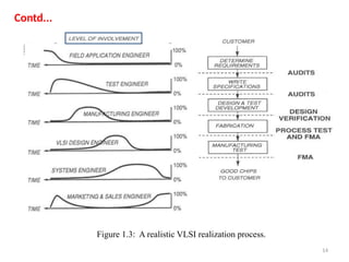
The VLSI realization process of Figure 1.3 has a distributed form of testing.
The dotted lines (representing screening) show testing.
Depending on the context, we give testing different names.
Requirements and specifications are audited, design and tests are verified,
and fabricated parts are tested.
Each testing level performs two functions, and involves different technical
personnel.
Contd...
15
Contd...
The first functionascertains that the work still conforms to the objectives of
previous levels and meets customer requirements.
The second ascertains that things have been done according to the capabilities
of the later process levels.
For example, verification of design and test procedures should ensure that the
design meets all functional and other specifications, and that it is also
manufacturable, testable, and repairable.
Figure 1.3 also shows the level of involvement of various types of engineering
personnel through the lifetime of a VLSI device.
While this figure is typical for an application specific integrated circuit
(ASIC), it applies to many other electronic devices as well.
The process begins with a dialogue between the customer and the marketing
engineer.
16.
16
Contd...
As specifications areprepared, some involvement of those responsible for later
activities (design, manufacture, and test) is advisable to ensure realizable specification.
The systems engineer then begins by constructing an architectural block diagram.
The architecture is verified by high-level simulation and each block is synthesized at
the logic-level.
The logic circuit is simulated for the same stimuli (often produced by testbenches) as
used for the high-level simulation.
A test-bench is hardware description language (HDL) code that, when executed,
produces stimuli for the designed circuit.
Vectors generated by testbenches are compacted or augmented and run through a
fault simulator to satisfy some specified fault coverage requirement.
The VLSI design engineer generates a layout and verifies the timing against the
specification.
17.
17
Contd...
Manufacturing and testengineers then fabricate and test wafers, and
package and test chips.
All through this process, any failure modes are identified and process
improvements are made to ensure a high yield of good devices.
Finally, the sales and field application engineers interact with the
customer.
As “verification and test” related activities are distributed throughout
the lifetime of the device, it is necessary that all engineering personnel have
the knowledge of test principles.
18.
18
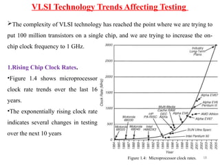
The complexity ofVLSI technology has reached the point where we are trying to
put 100 million transistors on a single chip, and we are trying to increase the on-
chip clock frequency to 1 GHz.
VLSI Technology Trends Affecting Testing
Figure 1.4: Microprocessor clock rates.
1.Rising Chip Clock Rates.
•Figure 1.4 shows microprocessor
clock rate trends over the last 16
years.
•The exponentially rising clock rate
indicates several changes in testing
over the next 10 years
19.
19
At-Speed Testing :It has been established that stuck-fault tests are more
effective when
applied at the circuit’s rated clock speed, rather than at a lower speed.
•Stuck-fault testing covers all (or most) circuit signals assuming that a faulty
signal may be permanently stuck-at logic 0 or 1.
•For a reliable high-speed test,the automatic test equipment (ATE) must
operate as fast as, or faster than, the circuit-under-test (CUT.)
2.ATE Cost
•In the year 2000, a state of the art ATE can apply vectors at a clock rate
of 1 GHz.
•The cost of such a tester rises roughly at the rate of $3,000 per pin.
•In addition, there is a fixed cost of function generators needed for mixed-
signal circuits that can range between 0.5–1.2 million dollars.
Contd...
20.
20
•Thus, devices withrated speed up to 1 GHz can be tested, though at a high
cost.
•The semiconductor industry, however, faces two types of problems.
•First, the installed test capability in many factories around the world still
allows only about a 100 MHz clock rate.
• By the time the present equipment is replaced by new systems, clock rates of
chips are likely to go beyond 1 GHz.
•Second, the microprocessor clock rate in the year 2000 has already approached
1 GHz, exceeding the present state of the art of the ATE.
Contd...
21.
21
3.Electro Magnetic Interference(EMI)
•A chip operating in the GHz frequency range must be tested for electromagnetic
interference (EMI).
•This is a problem because inductance in the wiring becomes active at these higher
frequencies, whereas it could be ignored at lower frequencies.
The inherent difficulties are:
1. Ringing in signal transitions along the wiring, because signal transitions are reflected
from the ends of a bus and bounce back to the source, where they are reflected again.
2. Interference with signal propagation through the wiring caused by the dielectric
permeability and the dielectric permittivity of the chip package.
3. Delay testing of paths requires propagation of sharp signal transitions, resulting in
high-frequency currents through interconnects, causing radiation coupling.
Contd...
22.
22
4.Increasing Transistor Density
Transistorfeature sizes on a VLSI chip reduce roughly by 10.5% per year,
resulting in a transistor density increase of roughly 22.1% every year.
1. Test complexity
Testing difficulty increases as the transistor density increases. This occurs
because the internal chip modules (particularly embedded memories)
become increasingly difficult to access.
2. Feature scaling and power dissipation
The power density (power dissipation per unit area) of a CMOS chip is
given by
Contd...
23.
23
1. Verification testingmust check for power buses overloaded by excessive
current. This causes a brown-out in the chip, just as overloading the electric
power distribution network in a city causes a drop in supply voltage. This
might cause the chip power bus lines to burn out due to metal migration, just
as an old-fashioned fuse burns out in a fuse box.
2. Application of the test vectors may cause excessive power dissipation on
the chip and burn it out, so the vectors must be adjusted to reduce power.
3. Shrinking features will eventually require the design of transistors with
reduced threshold voltage. These devices have higher leakage current, which
reduces the effectiveness of testing.
Contd...
24.
24
5.Current testing
•A verysuccessful recent approach to test chips is to check for elevated
quiescent current.
•This method is called IDDQ(quiescent Idd) testing.
•While switching, CMOS circuits exhibit an elevated current in the digital logic,
which dies out quickly to a small quiescent current (IDDQ) after the gate output
settles to a steady state.
•Faults, such as transistors stuck-on, shorted wires, shorts from transistor gates to
drains, etc., elevate the quiescent current. IDDQ testing marks the chip as faulty if the
measured quiescent current through ground busses of the chip exceeds a pre-specified
threshold.
6.Integration of Analog and Digital Devices onto One Chip
Integration onto one chip eliminates a significant delay, but brings new issues of
testing mixed-signal circuits on one chip.
Contd...
25.
25
Types of Testing
Characterizationtesting, design debug or verification testing Performed on new
designs -- determines if design is correct and meets ALL specifications -- labor
intensive.
AC, DC and functional tests performed. Probing of internal chip nodes may also be
performed.
Specialized tools are used, such as scanning electron microscopes (SEM) and
electron beam tests.
The process is designed to (1) diagnose and correct errors, (2) set the final
specifications and (3) is used to develop a production test program.
Less intensive characterization test performed during normal life-cycle of chip to
improve design and process yield.
Yield: Fraction of acceptable parts among all fabricated parts.
26.
26
Contd...
Production (go/no-gotest)
Shorter and less intensive test performed on every chip.
Enforces quality requirements by determining if chip specifications are met.
Main driver is cost -- test time MUST be minimized.
Tests must have high coverage of modeled faults.
No fault diagnosis, only an outgoing inspection test which verifies all relevant
specifications.
Some chips that pass production test will fail very quickly thereafter.
Burn-in ensures reliability by forcing failure in these "weak" chips. Key is to
accelerate the failure mechanisms by increasing temperature and/or voltage
while applying test patterns.
Burn-in or stress test
27.
27
Two types offailures are isolated by burn-in:
Infant mortality failures:
• Often caused by a combination of sensitive design and process variations.
• Short-term burn-in effective (10-30 hours).
Freak failures:
• Same failure mechanisms as reliable devices. Long burn-in time required (100-
1000 hours).
• Very expensive.
System manufacturers perform before incorporating chips into systems.
Once inserted, the cost of discovery can be much higher than cost of the
inspection test.
The rule of Ten: The cost of discovering a defective chip increases by an order of
magnitude at each successive level of integration, from die/package, board and
system.
Incoming Inspection
Contd...
28.
28
Can be similaror more comprehensive than production test.
Incoming inspection can be performed on a random sample of chips.
Contd...
DC parametric tests include shorts test, opens test, leakage test, etc.
AC parametric tests include delay test, setup and hold test, etc.
Input vectors and corresponding responses designed to check proper operation of a
verified design.
Structural tests that target specific faults on internal nodes of the chip. Often achieve
high coverage of the modelled faults (>95%).
Functional vectors, on the other hand, often refer to verification vectors designed to
determine if hardware matches specification.
Typically they have low fault coverage (<70%).
Parametric tests:
•Functional tests: