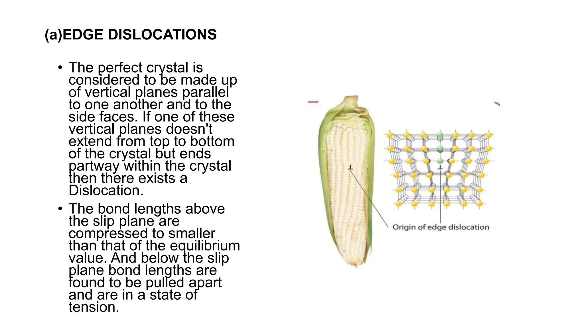
2. WHY SHOULD WE STUDY CRYSTAL
IMPERFECTIONS?
Technically important properties such as mechanical strength.
Ductility, Crystal growth, conduction in Semiconductors are
greatly affected by relatively minor changes in crystal Structure
caused by DEFECTS/ IMPERFECTIONS.
3. • Crystal Imperfections are the defects in the regular geometrical
arrangement of the atoms in a Crystalline solid.
• A Perfect Crystal is an idealization; there is no such thing in
nature.
• The defects may be the results of the crystal deformation or
rapid cooling from high temperature or high energy radiation
striking the solid.
• The defects influence the mechanical, electrical, and optical
behavior of the crystal.
4. • The imperfections may be classified widely as:
• Point Defects
• Line Defects
• Surface Defects
• Volume Defects
5. Point Defects
• These are the lattice errors at isolated points, takes place due
to the imperfect packing of atoms during crystallization or due to
the vibrations of atoms at high temperatures.
6. (a)VACANCIES
A simplest point defects
in a crystal. Refers to
missing atom or vacant
atomic site. Arise either
from imperfect packing
during original
crystallization or from
thermal vibrations at
high temperatures.
7. (b)FRENKEL DEFECT
• It is formed by a cat ion leaving its
normal position and moving into an
interstial site.
(c)SCHOTTKY DEFECT
It is formed by removing one cat ion
and one anion from the interior of
the crystal and then placing them
both at an external surface.
8. (d)COMPOSITIONAL
DEFECTS
• These arise from impurity
atoms during crystallisation.
They occur on lattice point as
a Substitutional impurity or as
an interstitial impurity.
• Substitutional impurity is
created when a foreign atom
substitutes for a parent atom
in the crystal lattice.
• Interstitial impurity is a small
sized foreign atom occupying
an interstitial position
between the regularly
positioned atoms.
9. (e) ELECTRONIC
DEFECTS
These are the errors in
charge distribution in
solids. These are primarily
necessary in electrical
conductivity & related
phenomenon
Prominent example is pn
junction formation and
transistor junction
formations.
10. 2. LINE IMPERFECTIONS/ DISLOCATIONS
• 1-D defects around which some of the atoms are misaligned.
• These are responsible for the useful property of ductility in metals,
ceramics and crystalline polymers.
• Types:- Edge Dislocations and Screw Dislocations.
11. (a)EDGE DISLOCATIONS
• The perfect crystal is
considered to be made up
of vertical planes parallel
to one another and to the
side faces. If one of these
vertical planes doesn't
extend from top to bottom
of the crystal but ends
partway within the crystal
then there exists a
Dislocation.
• The bond lengths above
the slip plane are
compressed to smaller
than that of the equilibrium
value. And below the slip
plane bond lengths are
found to be pulled apart
and are in a state of
tension.