Download to read offline
![International INTERNATIONAL Journal of Electronics and Communication JOURNAL Engineering OF ELECTRONICS & Technology (IJECET), AND
ISSN 0976 –
6464(Print), ISSN 0976 – 6472(Online), Volume 5, Issue 10, October (2014), pp. 74-79 © IAEME
COMMUNICATION ENGINEERING & TECHNOLOGY (IJECET)
ISSN 0976 – 6464(Print)
ISSN 0976 – 6472(Online)
Volume 5, Issue 10, October (2014), pp. 74-79
© IAEME: http://www.iaeme.com/IJECET.asp
Journal Impact Factor (2014): 7.2836 (Calculated by GISI)
www.jifactor.com
74
IJECET
© I A E M E
COPPER NANOFILM ANTENNA FOR WLAN
APPLICATIONS
Rajendra R. Patil1, Vani R.M2, P.V. Hunagund3
1,3Department of Applied Electronics, Gulbarga University, Gulbarga-585106 India
2University Science Instrumentation Center, Gulbarga University, 585106 India
ABSTRACT
In this article we investigate the reliability of copper nanofilm as radiating patch on FR4
substrate for radiation properties. Pure copper is deposited through RF-sputter system at room
temperature to a thickness around 100 nm on 1.6 mm height FR4 dielectric substrate to produce a 5.8
GHz nanofilm antenna. The effect of ultrathin copper metallization i.e. on antenna parameters such
as resonant frequency, return loss, bandwidth and gain are investigated. The nanofilm antenna is
compared with bulk copper patch of 17 micron thickness of antenna. It is found that nanofilm
antenna presents wide bandwidth, higher return loss and slightly decreased gain over bulk patch
antenna. The nanofilm antenna finds applications in, such as wireless LAN where short distance
higher data rate transmission is required. The results encourage incorporating metallic nanofilm as a
radiating element of an antenna for wide bandwidth improvement.
Keywords: Copper Nanofilm, Skin Depth, Patch Antenna, Wireless LAN.
1. INTRODUCTION
Microstrip patch antennas (MPAs) are widely used radio frequency/microwave passive
devices in cellular communications, wireless sensor networks (WSN), wireless local area networks
(WLAN), global positioning systems (GPS) etc. The MPAs have advantages such as low profile,
light weight, low cost etc. The limitations of MPAs are narrow bandwidth, low gain, low efficiency
and low power handling capacity. Nowadays, there is a continuous expansion of wireless system
applications that demands higher bandwidth for high data rate transmission. The aim of this research
is to discuss the usability of conducting ultra thin copper metal nanofilm (around 100 nm) radiating
patch of antenna for bandwidth enhancement in wireless communication.
In this work, our study originates from previous work done in [1], where aperture coupled
microstrip antenna with different nanofilm metals like Aluminum, Chromium, Titanium and Nickel
patch were used. In this paper, we have considered other antenna structure with different metal
nanofilm. We have designed, simulated, and fabricated bulk and nanofilm copper patch antennas](https://image.slidesharecdn.com/coppernanofilmantennaforwlanapplications-141110054228-conversion-gate01/85/Copper-nanofilm-antenna-for-wlan-applications-1-320.jpg)
![International INTERNATIONAL Journal of Electronics and Communication JOURNAL Engineering OF ELECTRONICS & Technology (IJECET), AND
ISSN 0976 –
6464(Print), ISSN 0976 – 6472(Online), Volume 5, Issue 10, October (2014), pp. 74-79 © IAEME
COMMUNICATION ENGINEERING & TECHNOLOGY (IJECET)
ISSN 0976 – 6464(Print)
ISSN 0976 – 6472(Online)
Volume 5, Issue 10, October (2014), pp. 74-79
© IAEME: http://www.iaeme.com/IJECET.asp
Journal Impact Factor (2014): 7.2836 (Calculated by GISI)
www.jifactor.com
74
IJECET
© I A E M E
COPPER NANOFILM ANTENNA FOR WLAN
APPLICATIONS
Rajendra R. Patil1, Vani R.M2, P.V. Hunagund3
1,3Department of Applied Electronics, Gulbarga University, Gulbarga-585106 India
2University Science Instrumentation Center, Gulbarga University, 585106 India
ABSTRACT
In this article we investigate the reliability of copper nanofilm as radiating patch on FR4
substrate for radiation properties. Pure copper is deposited through RF-sputter system at room
temperature to a thickness around 100 nm on 1.6 mm height FR4 dielectric substrate to produce a 5.8
GHz nanofilm antenna. The effect of ultrathin copper metallization i.e. on antenna parameters such
as resonant frequency, return loss, bandwidth and gain are investigated. The nanofilm antenna is
compared with bulk copper patch of 17 micron thickness of antenna. It is found that nanofilm
antenna presents wide bandwidth, higher return loss and slightly decreased gain over bulk patch
antenna. The nanofilm antenna finds applications in, such as wireless LAN where short distance
higher data rate transmission is required. The results encourage incorporating metallic nanofilm as a
radiating element of an antenna for wide bandwidth improvement.
Keywords: Copper Nanofilm, Skin Depth, Patch Antenna, Wireless LAN.
1. INTRODUCTION
Microstrip patch antennas (MPAs) are widely used radio frequency/microwave passive
devices in cellular communications, wireless sensor networks (WSN), wireless local area networks
(WLAN), global positioning systems (GPS) etc. The MPAs have advantages such as low profile,
light weight, low cost etc. The limitations of MPAs are narrow bandwidth, low gain, low efficiency
and low power handling capacity. Nowadays, there is a continuous expansion of wireless system
applications that demands higher bandwidth for high data rate transmission. The aim of this research
is to discuss the usability of conducting ultra thin copper metal nanofilm (around 100 nm) radiating
patch of antenna for bandwidth enhancement in wireless communication.
In this work, our study originates from previous work done in [1], where aperture coupled
microstrip antenna with different nanofilm metals like Aluminum, Chromium, Titanium and Nickel
patch were used. In this paper, we have considered other antenna structure with different metal
nanofilm. We have designed, simulated, and fabricated bulk and nanofilm copper patch antennas](https://image.slidesharecdn.com/coppernanofilmantennaforwlanapplications-141110054228-conversion-gate01/75/Copper-nanofilm-antenna-for-wlan-applications-1-2048.jpg)
![International Journal of Electronics and Communication Engineering Technolo
6464(Print), ISSN 0976 – 6472(Online), Volume 5, Issue 10, October (2014), pp.
gy –
9 © IAEME
with proximity feeding technique. This technique enables nanofilm metallic patch coupling to bulk
microstrip feed line through electromagnetic
reliable contact between bulk and nano t
proximity coupled antenna as described in [2], has the largest bandwidth as high as 13 percent, is
easy to model and has low spurious radiation. However its fabrication is somewhat more difficult.
The length and width of the feeding strip line, and width
the impedance match for a particular frequency resonance.
using IE3D simulator which is based on method of
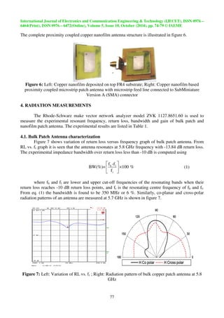
2. THE DESIGNED ANTENNA
radiation. This scheme also avoids
thickness metallic parts, like aperture coupled antenna
Figure 1: Geometry of 5.8 GHz
dimensions: 25251.6 mm3
FR4 substrates: 3.2 mm. Feedline dimensions
Rectangular patch dimensions
The proximity coupled antenna geometry is illustrated in figure 1
two layer substrate with the microstrip feed
patch antenna on the top substrate.
centre of the rectangular patch. The coupling between the patch and the microstrip line is capacitive
in nature [4]. Thus, this feeding technique is also
feed. The antenna dimensions shown in figure 1 are
IE3D simulator. The simulated result
30 dB, and a bandwidth of 582 MHz.
Figure 2: Left: Simulated return loss characteristics
Technology (IJECET), ISSN 0976
74-79
75
width-to-line ratio of the patch is used to control
The design and simulation was done by
moment (MoM) [3].
proximity coupled microstrip patch antenna
; bottom FR4 substrate: 35351.6 mm3.
wf f for 50 impedance match
Wp Lp: 1510 mm2
1. The antenna structure uses
line on the bottom substrate and the
The microstrip feed line terminates in an open end underneath the
known as “electromagnetically coupled
found by simulating the model ant
results shows antenna resonates at 5.79 GHz with a return loss of
Figure 2 illustrates simulated results.
characteristics; Right: Radiation pattern
having physical
antenna. The
antenna. Top FR4 substrate
The total height h of
match: mm2;
. rectangular metallic
coupled” microstrip
antenna using
-
at 5.79 GHz](https://image.slidesharecdn.com/coppernanofilmantennaforwlanapplications-141110054228-conversion-gate01/85/Copper-nanofilm-antenna-for-wlan-applications-2-320.jpg)
![International Journal of Electronics and Communication Engineering Technolo
6464(Print), ISSN 0976 – 6472(Online), Volume 5, Issue 10, October (2014), pp.
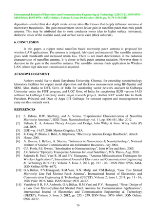
3. ANTENNA FABRICATION
3.1 Bulk Patch Antenna Fabrication
The bulk antenna is fabricated using photolithographic process. As per dimensions listed in
figure 1, the copper clad (17 micron t
ground. The bulk copper (17 micron thickness)
FR4 substrate. The fabricated antenna
thickness) FR4 PCB is etched for microstrip feed line and
is listed in figure 4.
Figure 4: Fabricated Proximity coupled
copper patch on top FR4 substrate
bulk patch antenna; Left: Bottom substrate;
substrate; Right: The antenna structure with SMA connector
3.2 Nanofilm Patch Antenna Fabrication
antenna of 15 mm2 is etched
Since, bottom FR4 substrate with bulk copper microstrip feed line and groun
is used for both bulk patch antenna and nanofilm patch antenna, we fabricate only nanofilm antenna
on FR4 substrate. The copper nanofilm patch antenna is fabricated by RF
pure copper for a thickness around 100 nm on FR4 substrate at room temperature.
thickness of the deposited copper nanofilm on FR4 substrate is about 104 nm
Scanning Electron Microscopy (SEM)
Figure 5: SEM micrograph showing deposited
Technology (IJECET), ISSN 0976
74-79
76
RF-sputtered deposition
[6] as shown in the figure 5.
copper in nanometer thickness
surface
gy –
9 © IAEME
hickness) on top of upper
; Centre: bulk
; ground metallization
(5) of
The average
nm, confirmed by
on FR4 substrate](https://image.slidesharecdn.com/coppernanofilmantennaforwlanapplications-141110054228-conversion-gate01/85/Copper-nanofilm-antenna-for-wlan-applications-3-320.jpg)
![International Journal of Electronics and Communication Engineering Technolo
6464(Print), ISSN 0976 – 6472(Online), Volume 5, Issue 10, October (2014), pp.
Technology (IJECET), ISSN 0976
gy –
9 © IAEME
74-79
The gain of the bulk thickness patch antenna is calculated using absolute method is given by
the relation [4]
P
r
0
P](https://image.slidesharecdn.com/coppernanofilmantennaforwlanapplications-141110054228-conversion-gate01/85/Copper-nanofilm-antenna-for-wlan-applications-5-320.jpg)

The document describes a study investigating copper nanofilm as a radiating patch for antenna applications. A 100nm thick copper nanofilm patch antenna and a 17micron thick bulk copper patch antenna were designed and fabricated on FR4 substrates. The nanofilm antenna was found to have a wider bandwidth (810MHz vs 350MHz for bulk antenna), higher return loss (-13.59dB vs -13.84dB for bulk antenna), and slightly lower gain. The increased bandwidth of the nanofilm antenna makes it suitable for applications requiring high data rate transmission such as wireless LAN. The results encourage the use of metallic nanofilms as radiating elements for antennas to improve bandwidth.