SlideShare a Scribd company logo
1 of 46
Download to read offline
1
FUNCTIONS OF COMBINATIONAL LOGIC
INTRODUCTION
‰ Digital systems obtain binary-coded data and
information that are continuously being operated on in
some manner.
‰ Many functions such as :
1) decoding and encoding-changing the data from one type of
code to another,
2) multiplexing-selecting one out of several groups of data,
3) demultiplexing- distributing data to one of several destinations,
4) comparing the magnitudes of two binary numbers,
5) parity checking- to detect data errors and,
6) performing arithmetic operation.
‰ All these operations and others have been facilitated by
the availability of numerous ICs in the MSI (medium-
scale-integration) category.
2
DECODER
DECODER
‰A decoder is a logic circuit that accepts a set of inputs that represents a
binary number and activates only the output that corresponds to that
input number.
‰In other words, a decoder circuit looks at its inputs, determines which
binary number is present there, and activates the one output that
corresponds to that number; all other outputs remain inactive.
M-1
2
1
0
3
‰ Many decoders are designed to produce active -LOW
outputs, where only the selected output is LOW while all
others are HIGH.
‰ This would be indicated by the presence of small circles
on the output lines in the decoder diagram.
‰ Some decoders do not utilize all of the 2N possible input
codes but only certain ones.
‰ For example, a BCD-to-decimal decoder has a 4-bit
input code and ten output lines that correspond to the
ten BCD code groups 0000 through 1001.
‰ Decoders of this type are often designed so that if any of
the unused codes are applied to the input, none of the
outputs will be activated.
‰ Figure below shows the circuitry for a decoder with three
inputs and 23 =8 outputs.
‰ It uses all AND gates, and so the outputs are active-
HIGH.
4
3-line-to-8-line Decoder
7
0
2
1
5
4
3
6
A
B
C
(MSB)
(LSB)
A
B
C
O0
=
A
B
C
O1
=
A
B
C
O2
=
BA
C
O3
=
A
B
C
O4
=
A
B
C
O5
=
A
CB
O6
=
CBA
O7
=
0
O
1
O
7
O
2
O
4
O
3
O
6
O
5
O
5
Verification 3-line-to-8-line decoder
Inputs Outputs
C B A O0 O1 O2 O3 O4 O5 O6 07
0
0
0 0
0
0
0
0
0
0
1
1
0
0 0
0
0
0
0
0
1
0
1
0
0
0
1
0 0
0
0
0
0
0
0
0
0
0
0
0
1
1
0 1
0
0
0
0
0
0
1 0
0
0
1
0
0
0
0
0
1
0
1 0
0
1
0
0
0
0
0
0 1 0
1
1
1
0
1
1
0
0
0
0
0
0
0 1
6
Enable Inputs
‰ Some decoders have one or more ENABLE inputs that
are used to control the operation of the decoder.
‰ For example, refer to the decoder in Figure 8.3 and
visualize having a common ENABLE line connected to a
fourth input of each gate.
‰ With this ENABLE line held HIGH the decoder will
function normally and the A, B, C input code will
determine which output is HIGH.
‰ With ENABLE held LOW, however, all the outputs will be
forced to the LOW state regardless of the levels at the A,
B, C inputs.
‰ Thus, the decoder is ENABLED only if ENABLE is HIGH.
Figure 8.3(a) shows the logic diagram for the 74LS138
decoder as it appears in the Fairchild TTL Data Book.
7
1
1-
-of
of-
-8
8-
-Decoder with Enable Inputs
Decoder with Enable Inputs
1
E 2
E 3
E
7
O 6
O 1
O
2
O
3
O
4
O
5
O 0
O
6
O
7
O 5
O 4
O 3
O 2
O 1
O 0
O
1
E 2
E 3
E
8
Truth table
3
E
2
E
1
E OUTPUTS
Respond To
Input Code
A2A1A0
1
0
0
Disabled-
all HIGH
X
X
1
Disabled-
all HIGH
X
1
X
Disabled-
all HIGH
0
X
X
9
BCD
BCD-
-to
to-
-Decimal
Decimal Decoder
Decoder
6
O
7
O
5
O
4
O
3
O
2
O
1
O
0
O
9
O
8
O
10
BCD-TO-7-SEGMENT DECODER/DRIVERS
‰ Most digital equipment has some means for displaying
information in a form that can be understood readily by the
user or operator.
‰ This information is often numerical data, but can also be
alphanumeric (numbers and letters).
‰ One of the simplest and most popular methods for
displaying numerical digits uses a 7-segnent configuration
[Figure 8.5(a)] to form the decimal characters 0 through 9
and sometimes the hex characters A through F.
11
a
b
c
d
f
e
g
BCD
BCD-
-TO
TO-
-7
7-
-SEGMENT DECODER
SEGMENT DECODER
b, c,
f & g
a, b, d,
e & g
a, b, c,
d, & g
a, b, c,
d, e & f
b & c
a, b, c, d,
e, f & g
a, b, c, f
& g
a, c, d,
f & g
c, d, e
f & g
a, b & c
12
7446/47 Seven
7446/47 Seven-
-Segment decoder/drivers
Segment decoder/drivers
a
b
c
d
e
f
g
‰ The 7446/47 decoder/drivers are
designed to activate specific
segments even for non-BCD input
codes (greater than 1001).
‰ Figure 8.6(b) shows the activated
segment patterns for all possible
input codes from 0000 to1111.
‰ Note that an input code of 1111 (15)
will blank out all the segments.
‰ Seven-segment decoder/drivers
such as the 7446/47 are exceptions
to the rule that decoder circuits
activate only one output for each
combination of inputs.
13
Logic diagram to activate segment b
‰ The function table for the BCD-to-
Seven segment decoder shown in
Figure (a).
‰ The K-map used to simplify the
logic expressions for driving
segment b is shown in Figure (b)
table below and logic diagram in
Figure (c). Entries 10-15 are
“don’t cares” as usual.
BCD Seven segment code
D C B A a b c d e f g
0 0 0 0 0 1 1 1 1 1 1 0
1 0 0 0 1 0 1 1 0 0 0 0
2 0 0 1 0 1 1 0 1 1 0 1
3 0 0 1 1 1 1 1 1 0 0 1
4 0 1 0 0 0 1 1 0 0 1 1
5 0 1 0 1 1 0 1 1 0 1 1
6 0 1 1 0 0 0 1 1 1 1 1
7 0 1 1 1 1 1 1 0 0 0 0
8 1 0 0 0 1 1 1 1 1 1 1
9 1 0 0 1 1 1 1 0 0 1 1
Decimal
digit
1
1
X
1
A
B A
B BA A
B
1
0
X
1
C
D 1
1
X
X
1
0
X
X
C
D
DC
C
D
(b)
(b)
∑
=
+
+
+
+
+
+
+
=
,7.8.9)
(0,1,2,3,4
m
A
B
C
D
A
B
C
D
CBA
D
A
B
C
D
BA
C
D
A
B
C
D
A
B
C
D
A
B
C
D
b
(a)
(a)
(c)
(c)
C
+
)
B
⊕
A
(
=
C
+
AB
+
B
A
=
b
B
A ⊕
C
)
B
A
(
Y +
⊕
=
14
a
b
c
d
e
f
g
15
a
b
c
d
e
f
g
16
a
b
c
d
e
f
g
17
a
b
c
d
e
f
g
18
a
b
c
d
e
f
g
19
a
b
c
d
e
f
g
20
Encoder
‰ Most decoders accept an input code and produce a HIGH (or LOW) at
one and only one output line.
‰ In other words, we can say that a decoder identifies, recognizes, or
detects a particular code.
‰ The opposite of this decoding process is called encoding and is
performed by a logic circuit called an encoder.
‰ An encoder has a number of input lines, only one of which is activated at
a given time, and produces an N-bit output code, depending on which
input is activated.
‰ Figure 8.15 is the general diagram for and encoder with M inputs and N
outputs. Here the inputs are active- HIGH, which means they are normally
LOW
21
8-line-to-3-line Encoder
Left
unconnected
0
O
1
O
2
O
0
A
1
A
2
A
4
A
5
A
6
A
7
A
3
A3
A
22
8-line-to-3-line Encoder
0
O
1
O
2
O
0
A
1
A
2
A
4
A
5
A
6
A
7
A
3
A3
A
23
8-line-to-3-line Encoder
0
O
1
O
2
O
0
A
1
A
2
A
4
A
5
A
6
A
7
A
3
A
5
A
24
8-line-to-3-line Encoder
0
O
1
O
2
O
0
A
1
A
2
A
4
A
5
A
6
A
7
A
5
A
3
A
25
Effect of activating two or more inputs
simultaneously
0
O
1
O
2
O
0
A
1
A
2
A
4
A
5
A
6
A
7
A
3
A
5
A
3
A
26
Truth table for 8
Truth table for 8-
-line
line-
-to
to-
-3
3-
-line
line
Encoder
Encoder
Inputs Outputs
O2 O1 O0
X
X 1 1 1 1 1 1 1 0 0 0
X
X 0 1 1 1 1 1 1 0 0 1
X
X 1 0 1 1 1 1 1 0 1 0
X
X 1 1 0 1 1 1 1 0 1 1
X
X 1 1 1 0 1 1 1 1 0 0
X
X 1 1 1 1 0 1 1 1 0 1
X
X 1 1 1 1 1 0 1 1 1 0
X
X 1 1 1 1 1 1 0 1 1 1
0
A 1
A 2
A 3
A 4
A 5
A 6
A 7
A
27
Effect of activating two or more simultaneously
0
O
1
O
2
O
0
A
1
A
2
A
4
A
6
A
7
A
5
A
3
A
28
Priority Encoder
Priority Encoder
2
A
1
A
8
A
9
A
1
O
0
O
3
O
2
O
29
Verification of Priority Encoder
1
A 2
A 3
A 4
A 5
A 6
A 7
A 8
A 9
A 3
O 2
O 1
O 0
O
Inputs Outputs
1 1 1 1 1 1 1 1 1 1 1 1 1
X X X X X X X X 0 0 1 1 0
X X X X X X X 0 1 0 1 1 1
X X X X X X 0 1 1 1 0 0 0
X X X X X 0 1 1 1 1 0 0 1
X X X X 0 1 1 1 1 1 0 1 0
X X X 0 1 1 1 1 1 1 0 1 1
X X 0 1 1 1 1 1 1 1 1 0 0
X 0 1 1 1 1 1 1 1 1 1 0 1
0 1 1 1 1 1 1 1 1 1 1 1 0
30
Verification of Priority Encoder
1
A 2
A 3
A 4
A 5
A 6
A 7
A 8
A 9
A 3
O 2
O 1
O 0
O
Inputs Outputs
1 1 1 1 1 1 1 1 1 1 1 1 1
X X X X X X X X 0 0 1 1 0
X X X X X X X 0 1 0 1 1 1
X X X X X X 0 1 1 1 0 0 0
X X X X X 0 1 1 1 1 0 0 1
X X X X 0 1 1 1 1 1 0 1 0
X X X 0 1 1 1 1 1 1 0 1 1
X X 0 1 1 1 1 1 1 1 1 0 0
X 0 1 1 1 1 1 1 1 1 1 0 1
0 1 1 1 1 1 1 1 1 1 1 1 0
31
Logic Diagram
32
MULTIPLEXERS (DATA SELECTORS)
‰ A modern home stereo system may have a switch that selects
music from one of four sources:
9a cassette tape,
9a compact disc (CD),
9a turntable, or
9a radio.
‰ The switch selects one of the electronic signals from one of these
four sources and sends it to the power amplifier and speakers.
‰ In simple terms, this is what a multiplexer does; it selects one of
several input signals and passes it onto the output.
‰ A digital multiplexer
digital multiplexer or data selector
data selector is logic circuit that
accepts several digital data inputs and selects one of them at any
given time to pass on to the output.
‰ The routing of the desired data input to the output is controlled by
SELECT inputs (often referred to as ADDRESS inputs).
33
Multiplexers (Data Selectors)
9 Figure above shows the functional diagram of a general digital multiplexer (MUX).
9 The multiplexer acts like a digitally controlled multi-position switch where the digital
code applied to the SELECT inputs controls which data inputs will be switched to the
output.
9 For example, output Z will equal data input I0 for some particular SELECT input code;
9 Z will equal I1 for another particular SELECT input code; and so on.
9 Stated another way, a multiplexer selects 1 out of N input data sources and transmits
the selected data to a single output channel.
9 This is called multiplexing.
34
Basic Two
Basic Two-
-Input Multiplexer
Input Multiplexer
9 An example of where a two- input MUX could be used is in a
computer system that uses two different MASTER CLOCK signals:
9 a high-speed clock( say 10 MHz ) for some programs, and
9 a slow-speed clock (say 4.77 MHz) for others.
9 Using the circuit of figure above, the 10-MHz clock would be tied to
I0 and the 4.77 MHz clock to I1.
9 A signal from the computer's control logic section would drive the
SELECT input to control which clock signal appears at output Z for
routing to the other computer circuits.
0
I
Z =
1
I
Z =
S Output
0
1
S
I
S
I
Z 1
0 ⋅
+
⋅
=
35
Four
Four-
-Input Multiplexer
Input Multiplexer
9 Here there are four inputs, which are selectively transmitted to the output
according to the four possible combinations of the S1S0 select inputs.
9 Each data input is gated with a different combination of select input levels.
9 I0 is gated with S1S0 so that I0 will pass through its AND gate to output Z only
when S1 = 0 and S0 = 0.
9 The table in the figure gives the outputs for the other three input select
codes.
0
I
Z =
1
I
Z =
2
I
Z =
3
I
Z =
S1 S0 Output
0 0
0 1
1 0
1 1
36
Eight
Eight-
- Input Multiplexer
Input Multiplexer
‰ This multiplexer has an enable input,
E, and provides both the normal and
inverted outputs.
‰ When E =0, the select inputs S2S1S0
will select one data input (from I0
through I7) for passage to output Z.
‰ when E=1, the multiplexer is
disabled so that Z= 0 regardless of
the select input code.
‰ This operation is summarized in
figure (b), and the 74151 logic
symbol is shown in figure (c).
Z Z
E
(b)
(c)
37
Example on Application of Multiplexer
Parallel-to-Serial Conversion
‰ One method for performing this parallel-to-serial
conversion uses a multiplexer, as illustrated in Figure (a).
‰ The data are present in parallel form at the outputs of the
X register and are to the eight-input multiplexer.
‰ A 3-bit (MOD-8) counter is used to provide the select code
bits S2S1S0 so that they cycle through from 000 to 111 as
clock pulses are applied.
‰ In this way, the output of the multiplexer will be X0
during the first clock period, X1 during the second clock
period, and so on.
‰ The output Z is a waveform which is a serial
representation of the parallel input data.
‰ The waveforms in the figure (b) are for the case where
X7X6X5X4X3X2X1X0 = 10110101.
‰ This conversion ­process takes a total of eight clock
cycles. Note that X0 (the LSB) is transmitted first and the
X7(MSB) is transmitted last. Figure (a) parallel-to-serial converter;
(b) waveforms X7X6X5X4X3X2X1X0 = 10110101
a)
a)
b)
b)
38
DEMULTIPLEXERS (DATA DISTRIBUTORS)
9 A multiplexer takes several inputs and transmits one of them to the output.
9 A Demultiplexer performs the reverse operation; it takes a single input and
distributes it over several outputs.
9 Figure above shows the functional diagram for a digital Demultiplexer (DEMUX).
9 The select input code determines to which output the DATA input will be
transmitted.
9 In other words, the Demultiplexer takes one input data source and selectively
distributes it to 1 of N output channels just like a multiposition switch.
39
1
1-
-Line
Line-
-to
to-
-4
4-
-Line Demultiplexer
Line Demultiplexer
‰Figure (a) shows a 1-line-to-4-line
demultiplexer circuits.
‰The input data line goes to all of the
AND gates.
‰The two select lines S0 and S1
enable only one gate at a time, and
the data appearing on the input line
will pass through the selected gate
to the associated output line.
0
1
0 S
S
I
O ⋅
⋅
=
0
1
1 S
S
I
O ⋅
⋅
=
0
1
2 S
S
I
O ⋅
⋅
=
0
1
3 S
S
I
O ⋅
⋅
=
SELECT
SELECT
Code
Code
OUTPUTS
OUTPUTS
S1 S0 O3 O2 O1 O0
0 0 0 0 0 I
0 1 0 0 I 0
1 0 0 I 0 0
1 1 I 0 0 0
(a)
1
1-
-Line
Line-
-to
to-
-8
8-
-Line Demultiplexer
Line Demultiplexer
40
9 The Demultiplexer circuit of figure above is very similar to the 3-line-to-8-line decoder circuit in figure of
1-of-8 decoder except that a fourth input (I) has been added to each gate.
9 It was pointed out earlier that many IC decoders have an ENABLE input, which is an extra input added to the
decoder gates.
9 This type of decoder chip can therefore be used as a Demultiplexer, with the binary code inputs (e.g., A, B,
C in figure of 1-of-8 decoder) serving as the SELECT inputs and the ENABLE input serving as the data input I.
9 For this reason, IC manufacturers often call this type of device a decoder/Demultiplexer, and it can be used
for either function.
( )
0
1
2
0
S
S
S
I
O ⋅
=
( )
0
1
2
1
S
S
S
I
O ⋅
=
( )
0
1
2
7
S
S
S
I
O ⋅
=
( )
0
1
2
6
S
S
S
I
O ⋅
=
( )
0
1
2
5
S
S
S
I
O ⋅
=
( )
0
1
2
4
S
S
S
I
O ⋅
=
( )
0
1
2
3
S
S
S
I
O ⋅
=
( )
0
2
2
S
S
S
I
O 1
⋅
=
6
O
7
O 5
O 4
O 3
O 2
O 1
O 0
O
1
E 2
E 3
E
41
Verification of 1
Verification of 1-
-line
line-
-to
to-
-8
8-
-line DEMULTIPLEXER
line DEMULTIPLEXER
SELECT Code OUTPUTS
S2 S1 S0 O7 O6 O5 O4 O3 O2 O1 0O
0 0 0 0 0 0 0 0 0 0 1
0 0 1 0 0 0 0 0 0 1 0
0 1 0 0 0 0 0 0 1 0 0
0 1 1 0 0 0 0 1 0 0 0
1 0 0 0 0 0 1 0 0 0 0
1 0 1 0 0 1 0 0 0 0 0
1 1 0 0 1 0 0 0 0 0 0
1 1 1 1 0 0 0 0 0 0 0
42
Cascading MUX and DEMUX
MUX DEMUX
Example # 1: on Application of Demultiplexer
Clock Demultiplexer
‰Many applications of the demultiplexing
principle are possible.
‰Figure below shows the 74LS138
demultiplexing being used as a clock
demultiplexer.
‰Under control of the SELECT lines, the clock
signal is routed to the desired destinations.
‰For example, with S2S1S0=000, the clock signal
applied to I will appear at output .
‰With S2S1S0=110, the clock will appear at .
6
O
7
O 5
O 4
O 3
O 2
O 1
O 0
O
0
O
6
O
Figure Clock Demultiplexer transmits clock
signal to a destination determined by select
code inputs
43
44
Security Monitoring System
‰Consider the case of a security monitoring system
in an industrial plant where the open/closed
status of many access door­s is to be monitored.
‰Each door controls the state of a switch, and it is
necessary to display ­the state of each switch on
LEDs that are mounted on a remote monitoring
panel at the security guard's station.
‰One way to do this would be to run a separate
signal from each door switch to an LED on the
monitoring panel.
‰This would require running many wires over a
long distance.
‰A better approach that would reduce the amount
of wiring to the monitoring panel uses a
multiplexer/demultiplexer combination.
‰Figure shows a system that can handle eight
doors, but the basic idea can be expanded to any
number.
Z
6
O
7
O
5
O
4
O
3
O
2
O
1
O
0
O
Ω
330
Example #2: on Application of Demultiplexer
45
Circuit Operation
Circuit Operation
‰ The eight door switches are the data inputs to the MUX; they produce a HIGH when a door is open and
a LOW when it is closed.
‰ The MOD-8 counter provides the select inputs to the MUX and also to the DEMUX on the remote
monitoring panel.
‰ Each DEMUX output is connected to an indicator LED that will be on when the output is LOW. Clock
pulses applied to the counter will cause the select in­puts to sequence through all of the possible
states 000 through 111. At each number of the counter, the switch status for the door of the same
number will be inverted by the MUX and passed to output. From there it is transmitted to the DEMUX
input, which passes it through to the output corresponding to the same number.
‰ For example, let's say that the counter is at the count of 110 (6). While the counter is in this state,
let's say that door 6 is closed. The LOW at I6 will pass through the MUX and be inverted to produce a
HIGH at .
‰ This HIGH will be passing through the DEMUX to output so that LED 6 will be off, indicating that
door 6 is closed.
‰ Now let's say that door 6 is open. A LOW will appear at and so that LED 6 will be on to signal
that door 6 is open.
‰ Of course, all other LEDs will be off during this time since is the only active output.
Z
6
O
6
O
Z
6
O
Circuit operation continued
46
‰As the counter is clocked through its eight states 000 through 111, the LEDs will
sequentially indicate the status of the eight doors.
‰If all the doors are closed, none of the LEDs will be on even when the
corresponding DEMUX output is selected.
‰If a door is open, its LED will turn on only during the time interval that the
counter is at the appropriate count; it will be off at all other counts.
‰Thus, the LED will be flashing on and off if its door is open.
‰The flashing rate can be adjusted by changing the frequency of the clock.
‰Note that there are only four signal lines going from the "door sensing" circuitry
to the remote monitoring panel: the output and the three select lines.
‰This is a saving of four lines when compared with the alternative of having one
line per door.
‰The MUX/DEMUX combination is used to transmit the status of each door to its
LED one at a time (serially) instead of all at once (parallel).
Z

More Related Content

Similar to 4,encoder & decoder MUX and DEMUX EEng - Copy.pdf

Electrónica digital: Display de 7 segmentos con compuertas lógicas
Electrónica digital: Display de 7 segmentos con compuertas lógicasElectrónica digital: Display de 7 segmentos con compuertas lógicas
Electrónica digital: Display de 7 segmentos con compuertas lógicasSANTIAGO PABLO ALBERTO
 
Decoders
DecodersDecoders
DecodersRe Man
 
Combinational and sequential logic
Combinational and sequential logicCombinational and sequential logic
Combinational and sequential logicDeepak John
 
Ceng232 Decoder Multiplexer Adder
Ceng232 Decoder Multiplexer AdderCeng232 Decoder Multiplexer Adder
Ceng232 Decoder Multiplexer Addergueste731a4
 
DLD Lecture No 22 Decoder Circuit and Types of Decoder.pptx
DLD Lecture No 22 Decoder Circuit and Types of Decoder.pptxDLD Lecture No 22 Decoder Circuit and Types of Decoder.pptx
DLD Lecture No 22 Decoder Circuit and Types of Decoder.pptxSaveraAyub2
 
UNIT - II.pptx
UNIT - II.pptxUNIT - II.pptx
UNIT - II.pptxamudhak10
 
CSLA and WTM using GDI Technique
CSLA and WTM using GDI TechniqueCSLA and WTM using GDI Technique
CSLA and WTM using GDI TechniqueNishant Yaduvanshi
 
Digital Electronics (EC8392) UNIT-II -PPT-S.SESHA VIDHYA/ ASP/ECE
Digital Electronics (EC8392) UNIT-II -PPT-S.SESHA VIDHYA/ ASP/ECEDigital Electronics (EC8392) UNIT-II -PPT-S.SESHA VIDHYA/ ASP/ECE
Digital Electronics (EC8392) UNIT-II -PPT-S.SESHA VIDHYA/ ASP/ECESeshaVidhyaS
 
Logic Design - Chapter 5: Part1 Combinattional Logic
Logic Design - Chapter 5: Part1 Combinattional LogicLogic Design - Chapter 5: Part1 Combinattional Logic
Logic Design - Chapter 5: Part1 Combinattional LogicGouda Mando
 
Introduction to embedded system & density based traffic light system
Introduction to embedded system & density based traffic light systemIntroduction to embedded system & density based traffic light system
Introduction to embedded system & density based traffic light systemRani Loganathan
 
Digital VLSI - Unit 2.pptx
Digital VLSI - Unit 2.pptxDigital VLSI - Unit 2.pptx
Digital VLSI - Unit 2.pptxSanjaiPrasad
 
I semester Unit 4 combinational circuits.pptx
I semester Unit 4 combinational circuits.pptxI semester Unit 4 combinational circuits.pptx
I semester Unit 4 combinational circuits.pptxMayank Pandey
 

Similar to 4,encoder & decoder MUX and DEMUX EEng - Copy.pdf (20)

Electrónica digital: Display de 7 segmentos con compuertas lógicas
Electrónica digital: Display de 7 segmentos con compuertas lógicasElectrónica digital: Display de 7 segmentos con compuertas lógicas
Electrónica digital: Display de 7 segmentos con compuertas lógicas
 
Decoders
DecodersDecoders
Decoders
 
microprocessors
microprocessorsmicroprocessors
microprocessors
 
Unit 4 dica
Unit 4 dicaUnit 4 dica
Unit 4 dica
 
Mcsl 17 ALP lab manual
Mcsl 17 ALP lab manualMcsl 17 ALP lab manual
Mcsl 17 ALP lab manual
 
Assignment#4b
Assignment#4bAssignment#4b
Assignment#4b
 
Combinational and sequential logic
Combinational and sequential logicCombinational and sequential logic
Combinational and sequential logic
 
The decoder
The decoderThe decoder
The decoder
 
Ceng232 Decoder Multiplexer Adder
Ceng232 Decoder Multiplexer AdderCeng232 Decoder Multiplexer Adder
Ceng232 Decoder Multiplexer Adder
 
DLD Lecture No 22 Decoder Circuit and Types of Decoder.pptx
DLD Lecture No 22 Decoder Circuit and Types of Decoder.pptxDLD Lecture No 22 Decoder Circuit and Types of Decoder.pptx
DLD Lecture No 22 Decoder Circuit and Types of Decoder.pptx
 
Combinational circuits
Combinational circuitsCombinational circuits
Combinational circuits
 
B sc3 unit 4 combi..lckt
B sc3 unit 4 combi..lcktB sc3 unit 4 combi..lckt
B sc3 unit 4 combi..lckt
 
Analog to Digital Converter
Analog to Digital ConverterAnalog to Digital Converter
Analog to Digital Converter
 
UNIT - II.pptx
UNIT - II.pptxUNIT - II.pptx
UNIT - II.pptx
 
CSLA and WTM using GDI Technique
CSLA and WTM using GDI TechniqueCSLA and WTM using GDI Technique
CSLA and WTM using GDI Technique
 
Digital Electronics (EC8392) UNIT-II -PPT-S.SESHA VIDHYA/ ASP/ECE
Digital Electronics (EC8392) UNIT-II -PPT-S.SESHA VIDHYA/ ASP/ECEDigital Electronics (EC8392) UNIT-II -PPT-S.SESHA VIDHYA/ ASP/ECE
Digital Electronics (EC8392) UNIT-II -PPT-S.SESHA VIDHYA/ ASP/ECE
 
Logic Design - Chapter 5: Part1 Combinattional Logic
Logic Design - Chapter 5: Part1 Combinattional LogicLogic Design - Chapter 5: Part1 Combinattional Logic
Logic Design - Chapter 5: Part1 Combinattional Logic
 
Introduction to embedded system & density based traffic light system
Introduction to embedded system & density based traffic light systemIntroduction to embedded system & density based traffic light system
Introduction to embedded system & density based traffic light system
 
Digital VLSI - Unit 2.pptx
Digital VLSI - Unit 2.pptxDigital VLSI - Unit 2.pptx
Digital VLSI - Unit 2.pptx
 
I semester Unit 4 combinational circuits.pptx
I semester Unit 4 combinational circuits.pptxI semester Unit 4 combinational circuits.pptx
I semester Unit 4 combinational circuits.pptx
 

Recently uploaded

Software and Systems Engineering Standards: Verification and Validation of Sy...
Software and Systems Engineering Standards: Verification and Validation of Sy...Software and Systems Engineering Standards: Verification and Validation of Sy...
Software and Systems Engineering Standards: Verification and Validation of Sy...VICTOR MAESTRE RAMIREZ
 
APPLICATIONS-AC/DC DRIVES-OPERATING CHARACTERISTICS
APPLICATIONS-AC/DC DRIVES-OPERATING CHARACTERISTICSAPPLICATIONS-AC/DC DRIVES-OPERATING CHARACTERISTICS
APPLICATIONS-AC/DC DRIVES-OPERATING CHARACTERISTICSKurinjimalarL3
 
Gfe Mayur Vihar Call Girls Service WhatsApp -> 9999965857 Available 24x7 ^ De...
Gfe Mayur Vihar Call Girls Service WhatsApp -> 9999965857 Available 24x7 ^ De...Gfe Mayur Vihar Call Girls Service WhatsApp -> 9999965857 Available 24x7 ^ De...
Gfe Mayur Vihar Call Girls Service WhatsApp -> 9999965857 Available 24x7 ^ De...srsj9000
 
Oxy acetylene welding presentation note.
Oxy acetylene welding presentation note.Oxy acetylene welding presentation note.
Oxy acetylene welding presentation note.eptoze12
 
VIP Call Girls Service Kondapur Hyderabad Call +91-8250192130
VIP Call Girls Service Kondapur Hyderabad Call +91-8250192130VIP Call Girls Service Kondapur Hyderabad Call +91-8250192130
VIP Call Girls Service Kondapur Hyderabad Call +91-8250192130Suhani Kapoor
 
Biology for Computer Engineers Course Handout.pptx
Biology for Computer Engineers Course Handout.pptxBiology for Computer Engineers Course Handout.pptx
Biology for Computer Engineers Course Handout.pptxDeepakSakkari2
 
Past, Present and Future of Generative AI
Past, Present and Future of Generative AIPast, Present and Future of Generative AI
Past, Present and Future of Generative AIabhishek36461
 
High Profile Call Girls Nagpur Isha Call 7001035870 Meet With Nagpur Escorts
High Profile Call Girls Nagpur Isha Call 7001035870 Meet With Nagpur EscortsHigh Profile Call Girls Nagpur Isha Call 7001035870 Meet With Nagpur Escorts
High Profile Call Girls Nagpur Isha Call 7001035870 Meet With Nagpur Escortsranjana rawat
 
ZXCTN 5804 / ZTE PTN / ZTE POTN / ZTE 5804 PTN / ZTE POTN 5804 ( 100/200 GE Z...
ZXCTN 5804 / ZTE PTN / ZTE POTN / ZTE 5804 PTN / ZTE POTN 5804 ( 100/200 GE Z...ZXCTN 5804 / ZTE PTN / ZTE POTN / ZTE 5804 PTN / ZTE POTN 5804 ( 100/200 GE Z...
ZXCTN 5804 / ZTE PTN / ZTE POTN / ZTE 5804 PTN / ZTE POTN 5804 ( 100/200 GE Z...ZTE
 
CCS355 Neural Network & Deep Learning Unit II Notes with Question bank .pdf
CCS355 Neural Network & Deep Learning Unit II Notes with Question bank .pdfCCS355 Neural Network & Deep Learning Unit II Notes with Question bank .pdf
CCS355 Neural Network & Deep Learning Unit II Notes with Question bank .pdfAsst.prof M.Gokilavani
 
IVE Industry Focused Event - Defence Sector 2024
IVE Industry Focused Event - Defence Sector 2024IVE Industry Focused Event - Defence Sector 2024
IVE Industry Focused Event - Defence Sector 2024Mark Billinghurst
 
(ANVI) Koregaon Park Call Girls Just Call 7001035870 [ Cash on Delivery ] Pun...
(ANVI) Koregaon Park Call Girls Just Call 7001035870 [ Cash on Delivery ] Pun...(ANVI) Koregaon Park Call Girls Just Call 7001035870 [ Cash on Delivery ] Pun...
(ANVI) Koregaon Park Call Girls Just Call 7001035870 [ Cash on Delivery ] Pun...ranjana rawat
 
Artificial-Intelligence-in-Electronics (K).pptx
Artificial-Intelligence-in-Electronics (K).pptxArtificial-Intelligence-in-Electronics (K).pptx
Artificial-Intelligence-in-Electronics (K).pptxbritheesh05
 
College Call Girls Nashik Nehal 7001305949 Independent Escort Service Nashik
College Call Girls Nashik Nehal 7001305949 Independent Escort Service NashikCollege Call Girls Nashik Nehal 7001305949 Independent Escort Service Nashik
College Call Girls Nashik Nehal 7001305949 Independent Escort Service NashikCall Girls in Nagpur High Profile
 
Microscopic Analysis of Ceramic Materials.pptx
Microscopic Analysis of Ceramic Materials.pptxMicroscopic Analysis of Ceramic Materials.pptx
Microscopic Analysis of Ceramic Materials.pptxpurnimasatapathy1234
 
Model Call Girl in Narela Delhi reach out to us at 🔝8264348440🔝
Model Call Girl in Narela Delhi reach out to us at 🔝8264348440🔝Model Call Girl in Narela Delhi reach out to us at 🔝8264348440🔝
Model Call Girl in Narela Delhi reach out to us at 🔝8264348440🔝soniya singh
 
OSVC_Meta-Data based Simulation Automation to overcome Verification Challenge...
OSVC_Meta-Data based Simulation Automation to overcome Verification Challenge...OSVC_Meta-Data based Simulation Automation to overcome Verification Challenge...
OSVC_Meta-Data based Simulation Automation to overcome Verification Challenge...Soham Mondal
 
Call Girls Narol 7397865700 Independent Call Girls
Call Girls Narol 7397865700 Independent Call GirlsCall Girls Narol 7397865700 Independent Call Girls
Call Girls Narol 7397865700 Independent Call Girlsssuser7cb4ff
 
Gurgaon ✡️9711147426✨Call In girls Gurgaon Sector 51 escort service
Gurgaon ✡️9711147426✨Call In girls Gurgaon Sector 51 escort serviceGurgaon ✡️9711147426✨Call In girls Gurgaon Sector 51 escort service
Gurgaon ✡️9711147426✨Call In girls Gurgaon Sector 51 escort servicejennyeacort
 

Recently uploaded (20)

Software and Systems Engineering Standards: Verification and Validation of Sy...
Software and Systems Engineering Standards: Verification and Validation of Sy...Software and Systems Engineering Standards: Verification and Validation of Sy...
Software and Systems Engineering Standards: Verification and Validation of Sy...
 
APPLICATIONS-AC/DC DRIVES-OPERATING CHARACTERISTICS
APPLICATIONS-AC/DC DRIVES-OPERATING CHARACTERISTICSAPPLICATIONS-AC/DC DRIVES-OPERATING CHARACTERISTICS
APPLICATIONS-AC/DC DRIVES-OPERATING CHARACTERISTICS
 
Gfe Mayur Vihar Call Girls Service WhatsApp -> 9999965857 Available 24x7 ^ De...
Gfe Mayur Vihar Call Girls Service WhatsApp -> 9999965857 Available 24x7 ^ De...Gfe Mayur Vihar Call Girls Service WhatsApp -> 9999965857 Available 24x7 ^ De...
Gfe Mayur Vihar Call Girls Service WhatsApp -> 9999965857 Available 24x7 ^ De...
 
Oxy acetylene welding presentation note.
Oxy acetylene welding presentation note.Oxy acetylene welding presentation note.
Oxy acetylene welding presentation note.
 
VIP Call Girls Service Kondapur Hyderabad Call +91-8250192130
VIP Call Girls Service Kondapur Hyderabad Call +91-8250192130VIP Call Girls Service Kondapur Hyderabad Call +91-8250192130
VIP Call Girls Service Kondapur Hyderabad Call +91-8250192130
 
Biology for Computer Engineers Course Handout.pptx
Biology for Computer Engineers Course Handout.pptxBiology for Computer Engineers Course Handout.pptx
Biology for Computer Engineers Course Handout.pptx
 
Past, Present and Future of Generative AI
Past, Present and Future of Generative AIPast, Present and Future of Generative AI
Past, Present and Future of Generative AI
 
High Profile Call Girls Nagpur Isha Call 7001035870 Meet With Nagpur Escorts
High Profile Call Girls Nagpur Isha Call 7001035870 Meet With Nagpur EscortsHigh Profile Call Girls Nagpur Isha Call 7001035870 Meet With Nagpur Escorts
High Profile Call Girls Nagpur Isha Call 7001035870 Meet With Nagpur Escorts
 
ZXCTN 5804 / ZTE PTN / ZTE POTN / ZTE 5804 PTN / ZTE POTN 5804 ( 100/200 GE Z...
ZXCTN 5804 / ZTE PTN / ZTE POTN / ZTE 5804 PTN / ZTE POTN 5804 ( 100/200 GE Z...ZXCTN 5804 / ZTE PTN / ZTE POTN / ZTE 5804 PTN / ZTE POTN 5804 ( 100/200 GE Z...
ZXCTN 5804 / ZTE PTN / ZTE POTN / ZTE 5804 PTN / ZTE POTN 5804 ( 100/200 GE Z...
 
CCS355 Neural Network & Deep Learning Unit II Notes with Question bank .pdf
CCS355 Neural Network & Deep Learning Unit II Notes with Question bank .pdfCCS355 Neural Network & Deep Learning Unit II Notes with Question bank .pdf
CCS355 Neural Network & Deep Learning Unit II Notes with Question bank .pdf
 
IVE Industry Focused Event - Defence Sector 2024
IVE Industry Focused Event - Defence Sector 2024IVE Industry Focused Event - Defence Sector 2024
IVE Industry Focused Event - Defence Sector 2024
 
(ANVI) Koregaon Park Call Girls Just Call 7001035870 [ Cash on Delivery ] Pun...
(ANVI) Koregaon Park Call Girls Just Call 7001035870 [ Cash on Delivery ] Pun...(ANVI) Koregaon Park Call Girls Just Call 7001035870 [ Cash on Delivery ] Pun...
(ANVI) Koregaon Park Call Girls Just Call 7001035870 [ Cash on Delivery ] Pun...
 
Artificial-Intelligence-in-Electronics (K).pptx
Artificial-Intelligence-in-Electronics (K).pptxArtificial-Intelligence-in-Electronics (K).pptx
Artificial-Intelligence-in-Electronics (K).pptx
 
College Call Girls Nashik Nehal 7001305949 Independent Escort Service Nashik
College Call Girls Nashik Nehal 7001305949 Independent Escort Service NashikCollege Call Girls Nashik Nehal 7001305949 Independent Escort Service Nashik
College Call Girls Nashik Nehal 7001305949 Independent Escort Service Nashik
 
Microscopic Analysis of Ceramic Materials.pptx
Microscopic Analysis of Ceramic Materials.pptxMicroscopic Analysis of Ceramic Materials.pptx
Microscopic Analysis of Ceramic Materials.pptx
 
Model Call Girl in Narela Delhi reach out to us at 🔝8264348440🔝
Model Call Girl in Narela Delhi reach out to us at 🔝8264348440🔝Model Call Girl in Narela Delhi reach out to us at 🔝8264348440🔝
Model Call Girl in Narela Delhi reach out to us at 🔝8264348440🔝
 
OSVC_Meta-Data based Simulation Automation to overcome Verification Challenge...
OSVC_Meta-Data based Simulation Automation to overcome Verification Challenge...OSVC_Meta-Data based Simulation Automation to overcome Verification Challenge...
OSVC_Meta-Data based Simulation Automation to overcome Verification Challenge...
 
Exploring_Network_Security_with_JA3_by_Rakesh Seal.pptx
Exploring_Network_Security_with_JA3_by_Rakesh Seal.pptxExploring_Network_Security_with_JA3_by_Rakesh Seal.pptx
Exploring_Network_Security_with_JA3_by_Rakesh Seal.pptx
 
Call Girls Narol 7397865700 Independent Call Girls
Call Girls Narol 7397865700 Independent Call GirlsCall Girls Narol 7397865700 Independent Call Girls
Call Girls Narol 7397865700 Independent Call Girls
 
Gurgaon ✡️9711147426✨Call In girls Gurgaon Sector 51 escort service
Gurgaon ✡️9711147426✨Call In girls Gurgaon Sector 51 escort serviceGurgaon ✡️9711147426✨Call In girls Gurgaon Sector 51 escort service
Gurgaon ✡️9711147426✨Call In girls Gurgaon Sector 51 escort service
 

4,encoder & decoder MUX and DEMUX EEng - Copy.pdf

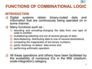
  • 1. 1 FUNCTIONS OF COMBINATIONAL LOGIC INTRODUCTION ‰ Digital systems obtain binary-coded data and information that are continuously being operated on in some manner. ‰ Many functions such as : 1) decoding and encoding-changing the data from one type of code to another, 2) multiplexing-selecting one out of several groups of data, 3) demultiplexing- distributing data to one of several destinations, 4) comparing the magnitudes of two binary numbers, 5) parity checking- to detect data errors and, 6) performing arithmetic operation. ‰ All these operations and others have been facilitated by the availability of numerous ICs in the MSI (medium- scale-integration) category.
  • 2. 2 DECODER DECODER ‰A decoder is a logic circuit that accepts a set of inputs that represents a binary number and activates only the output that corresponds to that input number. ‰In other words, a decoder circuit looks at its inputs, determines which binary number is present there, and activates the one output that corresponds to that number; all other outputs remain inactive. M-1 2 1 0
  • 3. 3 ‰ Many decoders are designed to produce active -LOW outputs, where only the selected output is LOW while all others are HIGH. ‰ This would be indicated by the presence of small circles on the output lines in the decoder diagram. ‰ Some decoders do not utilize all of the 2N possible input codes but only certain ones. ‰ For example, a BCD-to-decimal decoder has a 4-bit input code and ten output lines that correspond to the ten BCD code groups 0000 through 1001. ‰ Decoders of this type are often designed so that if any of the unused codes are applied to the input, none of the outputs will be activated. ‰ Figure below shows the circuitry for a decoder with three inputs and 23 =8 outputs. ‰ It uses all AND gates, and so the outputs are active- HIGH.
  • 5. 5 Verification 3-line-to-8-line decoder Inputs Outputs C B A O0 O1 O2 O3 O4 O5 O6 07 0 0 0 0 0 0 0 0 0 0 1 1 0 0 0 0 0 0 0 0 1 0 1 0 0 0 1 0 0 0 0 0 0 0 0 0 0 0 0 0 1 1 0 1 0 0 0 0 0 0 1 0 0 0 1 0 0 0 0 0 1 0 1 0 0 1 0 0 0 0 0 0 1 0 1 1 1 0 1 1 0 0 0 0 0 0 0 1
  • 6. 6 Enable Inputs ‰ Some decoders have one or more ENABLE inputs that are used to control the operation of the decoder. ‰ For example, refer to the decoder in Figure 8.3 and visualize having a common ENABLE line connected to a fourth input of each gate. ‰ With this ENABLE line held HIGH the decoder will function normally and the A, B, C input code will determine which output is HIGH. ‰ With ENABLE held LOW, however, all the outputs will be forced to the LOW state regardless of the levels at the A, B, C inputs. ‰ Thus, the decoder is ENABLED only if ENABLE is HIGH. Figure 8.3(a) shows the logic diagram for the 74LS138 decoder as it appears in the Fairchild TTL Data Book.
  • 7. 7 1 1- -of of- -8 8- -Decoder with Enable Inputs Decoder with Enable Inputs 1 E 2 E 3 E 7 O 6 O 1 O 2 O 3 O 4 O 5 O 0 O 6 O 7 O 5 O 4 O 3 O 2 O 1 O 0 O 1 E 2 E 3 E
  • 8. 8 Truth table 3 E 2 E 1 E OUTPUTS Respond To Input Code A2A1A0 1 0 0 Disabled- all HIGH X X 1 Disabled- all HIGH X 1 X Disabled- all HIGH 0 X X
  • 10. 10 BCD-TO-7-SEGMENT DECODER/DRIVERS ‰ Most digital equipment has some means for displaying information in a form that can be understood readily by the user or operator. ‰ This information is often numerical data, but can also be alphanumeric (numbers and letters). ‰ One of the simplest and most popular methods for displaying numerical digits uses a 7-segnent configuration [Figure 8.5(a)] to form the decimal characters 0 through 9 and sometimes the hex characters A through F.
  • 11. 11 a b c d f e g BCD BCD- -TO TO- -7 7- -SEGMENT DECODER SEGMENT DECODER b, c, f & g a, b, d, e & g a, b, c, d, & g a, b, c, d, e & f b & c a, b, c, d, e, f & g a, b, c, f & g a, c, d, f & g c, d, e f & g a, b & c
  • 12. 12 7446/47 Seven 7446/47 Seven- -Segment decoder/drivers Segment decoder/drivers a b c d e f g ‰ The 7446/47 decoder/drivers are designed to activate specific segments even for non-BCD input codes (greater than 1001). ‰ Figure 8.6(b) shows the activated segment patterns for all possible input codes from 0000 to1111. ‰ Note that an input code of 1111 (15) will blank out all the segments. ‰ Seven-segment decoder/drivers such as the 7446/47 are exceptions to the rule that decoder circuits activate only one output for each combination of inputs.
  • 13. 13 Logic diagram to activate segment b Logic diagram to activate segment b ‰ The function table for the BCD-to- Seven segment decoder shown in Figure (a). ‰ The K-map used to simplify the logic expressions for driving segment b is shown in Figure (b) table below and logic diagram in Figure (c). Entries 10-15 are “don’t cares” as usual. BCD Seven segment code D C B A a b c d e f g 0 0 0 0 0 1 1 1 1 1 1 0 1 0 0 0 1 0 1 1 0 0 0 0 2 0 0 1 0 1 1 0 1 1 0 1 3 0 0 1 1 1 1 1 1 0 0 1 4 0 1 0 0 0 1 1 0 0 1 1 5 0 1 0 1 1 0 1 1 0 1 1 6 0 1 1 0 0 0 1 1 1 1 1 7 0 1 1 1 1 1 1 0 0 0 0 8 1 0 0 0 1 1 1 1 1 1 1 9 1 0 0 1 1 1 1 0 0 1 1 Decimal digit 1 1 X 1 A B A B BA A B 1 0 X 1 C D 1 1 X X 1 0 X X C D DC C D (b) (b) ∑ = + + + + + + + = ,7.8.9) (0,1,2,3,4 m A B C D A B C D CBA D A B C D BA C D A B C D A B C D A B C D b (a) (a) (c) (c) C + ) B ⊕ A ( = C + AB + B A = b B A ⊕ C ) B A ( Y + ⊕ =
  • 20. 20 Encoder ‰ Most decoders accept an input code and produce a HIGH (or LOW) at one and only one output line. ‰ In other words, we can say that a decoder identifies, recognizes, or detects a particular code. ‰ The opposite of this decoding process is called encoding and is performed by a logic circuit called an encoder. ‰ An encoder has a number of input lines, only one of which is activated at a given time, and produces an N-bit output code, depending on which input is activated. ‰ Figure 8.15 is the general diagram for and encoder with M inputs and N outputs. Here the inputs are active- HIGH, which means they are normally LOW
  • 25. 25 Effect of activating two or more inputs simultaneously 0 O 1 O 2 O 0 A 1 A 2 A 4 A 5 A 6 A 7 A 3 A 5 A 3 A
  • 26. 26 Truth table for 8 Truth table for 8- -line line- -to to- -3 3- -line line Encoder Encoder Inputs Outputs O2 O1 O0 X X 1 1 1 1 1 1 1 0 0 0 X X 0 1 1 1 1 1 1 0 0 1 X X 1 0 1 1 1 1 1 0 1 0 X X 1 1 0 1 1 1 1 0 1 1 X X 1 1 1 0 1 1 1 1 0 0 X X 1 1 1 1 0 1 1 1 0 1 X X 1 1 1 1 1 0 1 1 1 0 X X 1 1 1 1 1 1 0 1 1 1 0 A 1 A 2 A 3 A 4 A 5 A 6 A 7 A
  • 27. 27 Effect of activating two or more simultaneously 0 O 1 O 2 O 0 A 1 A 2 A 4 A 6 A 7 A 5 A 3 A
  • 29. 29 Verification of Priority Encoder Verification of Priority Encoder 1 A 2 A 3 A 4 A 5 A 6 A 7 A 8 A 9 A 3 O 2 O 1 O 0 O Inputs Outputs 1 1 1 1 1 1 1 1 1 1 1 1 1 X X X X X X X X 0 0 1 1 0 X X X X X X X 0 1 0 1 1 1 X X X X X X 0 1 1 1 0 0 0 X X X X X 0 1 1 1 1 0 0 1 X X X X 0 1 1 1 1 1 0 1 0 X X X 0 1 1 1 1 1 1 0 1 1 X X 0 1 1 1 1 1 1 1 1 0 0 X 0 1 1 1 1 1 1 1 1 1 0 1 0 1 1 1 1 1 1 1 1 1 1 1 0
  • 30. 30 Verification of Priority Encoder 1 A 2 A 3 A 4 A 5 A 6 A 7 A 8 A 9 A 3 O 2 O 1 O 0 O Inputs Outputs 1 1 1 1 1 1 1 1 1 1 1 1 1 X X X X X X X X 0 0 1 1 0 X X X X X X X 0 1 0 1 1 1 X X X X X X 0 1 1 1 0 0 0 X X X X X 0 1 1 1 1 0 0 1 X X X X 0 1 1 1 1 1 0 1 0 X X X 0 1 1 1 1 1 1 0 1 1 X X 0 1 1 1 1 1 1 1 1 0 0 X 0 1 1 1 1 1 1 1 1 1 0 1 0 1 1 1 1 1 1 1 1 1 1 1 0
  • 32. 32 MULTIPLEXERS (DATA SELECTORS) MULTIPLEXERS (DATA SELECTORS) ‰ A modern home stereo system may have a switch that selects music from one of four sources: 9a cassette tape, 9a compact disc (CD), 9a turntable, or 9a radio. ‰ The switch selects one of the electronic signals from one of these four sources and sends it to the power amplifier and speakers. ‰ In simple terms, this is what a multiplexer does; it selects one of several input signals and passes it onto the output. ‰ A digital multiplexer digital multiplexer or data selector data selector is logic circuit that accepts several digital data inputs and selects one of them at any given time to pass on to the output. ‰ The routing of the desired data input to the output is controlled by SELECT inputs (often referred to as ADDRESS inputs).
  • 33. 33 Multiplexers (Data Selectors) Multiplexers (Data Selectors) 9 Figure above shows the functional diagram of a general digital multiplexer (MUX). 9 The multiplexer acts like a digitally controlled multi-position switch where the digital code applied to the SELECT inputs controls which data inputs will be switched to the output. 9 For example, output Z will equal data input I0 for some particular SELECT input code; 9 Z will equal I1 for another particular SELECT input code; and so on. 9 Stated another way, a multiplexer selects 1 out of N input data sources and transmits the selected data to a single output channel. 9 This is called multiplexing.
  • 34. 34 Basic Two Basic Two- -Input Multiplexer Input Multiplexer 9 An example of where a two- input MUX could be used is in a computer system that uses two different MASTER CLOCK signals: 9 a high-speed clock( say 10 MHz ) for some programs, and 9 a slow-speed clock (say 4.77 MHz) for others. 9 Using the circuit of figure above, the 10-MHz clock would be tied to I0 and the 4.77 MHz clock to I1. 9 A signal from the computer's control logic section would drive the SELECT input to control which clock signal appears at output Z for routing to the other computer circuits. 0 I Z = 1 I Z = S Output 0 1 S I S I Z 1 0 ⋅ + ⋅ =
  • 35. 35 Four Four- -Input Multiplexer Input Multiplexer 9 Here there are four inputs, which are selectively transmitted to the output according to the four possible combinations of the S1S0 select inputs. 9 Each data input is gated with a different combination of select input levels. 9 I0 is gated with S1S0 so that I0 will pass through its AND gate to output Z only when S1 = 0 and S0 = 0. 9 The table in the figure gives the outputs for the other three input select codes. 0 I Z = 1 I Z = 2 I Z = 3 I Z = S1 S0 Output 0 0 0 1 1 0 1 1
  • 36. 36 Eight Eight- - Input Multiplexer Input Multiplexer ‰ This multiplexer has an enable input, E, and provides both the normal and inverted outputs. ‰ When E =0, the select inputs S2S1S0 will select one data input (from I0 through I7) for passage to output Z. ‰ when E=1, the multiplexer is disabled so that Z= 0 regardless of the select input code. ‰ This operation is summarized in figure (b), and the 74151 logic symbol is shown in figure (c). Z Z E (b) (c)
  • 37. 37 Example on Application of Multiplexer Example on Application of Multiplexer Parallel-to-Serial Conversion ‰ One method for performing this parallel-to-serial conversion uses a multiplexer, as illustrated in Figure (a). ‰ The data are present in parallel form at the outputs of the X register and are to the eight-input multiplexer. ‰ A 3-bit (MOD-8) counter is used to provide the select code bits S2S1S0 so that they cycle through from 000 to 111 as clock pulses are applied. ‰ In this way, the output of the multiplexer will be X0 during the first clock period, X1 during the second clock period, and so on. ‰ The output Z is a waveform which is a serial representation of the parallel input data. ‰ The waveforms in the figure (b) are for the case where X7X6X5X4X3X2X1X0 = 10110101. ‰ This conversion ­process takes a total of eight clock cycles. Note that X0 (the LSB) is transmitted first and the X7(MSB) is transmitted last. Figure (a) parallel-to-serial converter; (b) waveforms X7X6X5X4X3X2X1X0 = 10110101 a) a) b) b)
  • 38. 38 DEMULTIPLEXERS (DATA DISTRIBUTORS) DEMULTIPLEXERS (DATA DISTRIBUTORS) 9 A multiplexer takes several inputs and transmits one of them to the output. 9 A Demultiplexer performs the reverse operation; it takes a single input and distributes it over several outputs. 9 Figure above shows the functional diagram for a digital Demultiplexer (DEMUX). 9 The select input code determines to which output the DATA input will be transmitted. 9 In other words, the Demultiplexer takes one input data source and selectively distributes it to 1 of N output channels just like a multiposition switch.
  • 39. 39 1 1- -Line Line- -to to- -4 4- -Line Demultiplexer Line Demultiplexer ‰Figure (a) shows a 1-line-to-4-line demultiplexer circuits. ‰The input data line goes to all of the AND gates. ‰The two select lines S0 and S1 enable only one gate at a time, and the data appearing on the input line will pass through the selected gate to the associated output line. 0 1 0 S S I O ⋅ ⋅ = 0 1 1 S S I O ⋅ ⋅ = 0 1 2 S S I O ⋅ ⋅ = 0 1 3 S S I O ⋅ ⋅ = SELECT SELECT Code Code OUTPUTS OUTPUTS S1 S0 O3 O2 O1 O0 0 0 0 0 0 I 0 1 0 0 I 0 1 0 0 I 0 0 1 1 I 0 0 0 (a)
  • 40. 1 1- -Line Line- -to to- -8 8- -Line Demultiplexer Line Demultiplexer 40 9 The Demultiplexer circuit of figure above is very similar to the 3-line-to-8-line decoder circuit in figure of 1-of-8 decoder except that a fourth input (I) has been added to each gate. 9 It was pointed out earlier that many IC decoders have an ENABLE input, which is an extra input added to the decoder gates. 9 This type of decoder chip can therefore be used as a Demultiplexer, with the binary code inputs (e.g., A, B, C in figure of 1-of-8 decoder) serving as the SELECT inputs and the ENABLE input serving as the data input I. 9 For this reason, IC manufacturers often call this type of device a decoder/Demultiplexer, and it can be used for either function. ( ) 0 1 2 0 S S S I O ⋅ = ( ) 0 1 2 1 S S S I O ⋅ = ( ) 0 1 2 7 S S S I O ⋅ = ( ) 0 1 2 6 S S S I O ⋅ = ( ) 0 1 2 5 S S S I O ⋅ = ( ) 0 1 2 4 S S S I O ⋅ = ( ) 0 1 2 3 S S S I O ⋅ = ( ) 0 2 2 S S S I O 1 ⋅ = 6 O 7 O 5 O 4 O 3 O 2 O 1 O 0 O 1 E 2 E 3 E
  • 41. 41 Verification of 1 Verification of 1- -line line- -to to- -8 8- -line DEMULTIPLEXER line DEMULTIPLEXER SELECT Code OUTPUTS S2 S1 S0 O7 O6 O5 O4 O3 O2 O1 0O 0 0 0 0 0 0 0 0 0 0 1 0 0 1 0 0 0 0 0 0 1 0 0 1 0 0 0 0 0 0 1 0 0 0 1 1 0 0 0 0 1 0 0 0 1 0 0 0 0 0 1 0 0 0 0 1 0 1 0 0 1 0 0 0 0 0 1 1 0 0 1 0 0 0 0 0 0 1 1 1 1 0 0 0 0 0 0 0
  • 42. 42 Cascading MUX and DEMUX Cascading MUX and DEMUX MUX DEMUX
  • 43. Example # 1: on Application of Demultiplexer Example # 1: on Application of Demultiplexer Clock Demultiplexer ‰Many applications of the demultiplexing principle are possible. ‰Figure below shows the 74LS138 demultiplexing being used as a clock demultiplexer. ‰Under control of the SELECT lines, the clock signal is routed to the desired destinations. ‰For example, with S2S1S0=000, the clock signal applied to I will appear at output . ‰With S2S1S0=110, the clock will appear at . 6 O 7 O 5 O 4 O 3 O 2 O 1 O 0 O 0 O 6 O Figure Clock Demultiplexer transmits clock signal to a destination determined by select code inputs 43
  • 44. 44 Security Monitoring System Security Monitoring System ‰Consider the case of a security monitoring system in an industrial plant where the open/closed status of many access door­s is to be monitored. ‰Each door controls the state of a switch, and it is necessary to display ­the state of each switch on LEDs that are mounted on a remote monitoring panel at the security guard's station. ‰One way to do this would be to run a separate signal from each door switch to an LED on the monitoring panel. ‰This would require running many wires over a long distance. ‰A better approach that would reduce the amount of wiring to the monitoring panel uses a multiplexer/demultiplexer combination. ‰Figure shows a system that can handle eight doors, but the basic idea can be expanded to any number. Z 6 O 7 O 5 O 4 O 3 O 2 O 1 O 0 O Ω 330
  • 45. Example #2: on Application of Demultiplexer Example #2: on Application of Demultiplexer 45 Circuit Operation Circuit Operation ‰ The eight door switches are the data inputs to the MUX; they produce a HIGH when a door is open and a LOW when it is closed. ‰ The MOD-8 counter provides the select inputs to the MUX and also to the DEMUX on the remote monitoring panel. ‰ Each DEMUX output is connected to an indicator LED that will be on when the output is LOW. Clock pulses applied to the counter will cause the select in­puts to sequence through all of the possible states 000 through 111. At each number of the counter, the switch status for the door of the same number will be inverted by the MUX and passed to output. From there it is transmitted to the DEMUX input, which passes it through to the output corresponding to the same number. ‰ For example, let's say that the counter is at the count of 110 (6). While the counter is in this state, let's say that door 6 is closed. The LOW at I6 will pass through the MUX and be inverted to produce a HIGH at . ‰ This HIGH will be passing through the DEMUX to output so that LED 6 will be off, indicating that door 6 is closed. ‰ Now let's say that door 6 is open. A LOW will appear at and so that LED 6 will be on to signal that door 6 is open. ‰ Of course, all other LEDs will be off during this time since is the only active output. Z 6 O 6 O Z 6 O
  • 46. Circuit operation continued 46 ‰As the counter is clocked through its eight states 000 through 111, the LEDs will sequentially indicate the status of the eight doors. ‰If all the doors are closed, none of the LEDs will be on even when the corresponding DEMUX output is selected. ‰If a door is open, its LED will turn on only during the time interval that the counter is at the appropriate count; it will be off at all other counts. ‰Thus, the LED will be flashing on and off if its door is open. ‰The flashing rate can be adjusted by changing the frequency of the clock. ‰Note that there are only four signal lines going from the "door sensing" circuitry to the remote monitoring panel: the output and the three select lines. ‰This is a saving of four lines when compared with the alternative of having one line per door. ‰The MUX/DEMUX combination is used to transmit the status of each door to its LED one at a time (serially) instead of all at once (parallel). Z