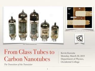
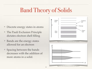
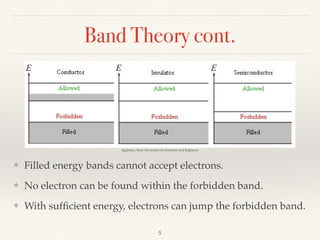
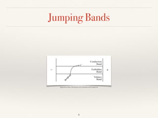
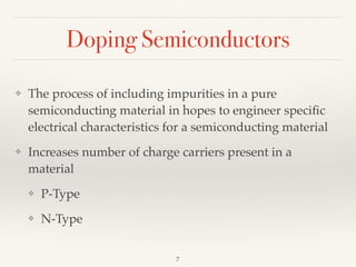
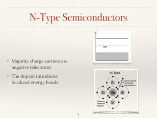
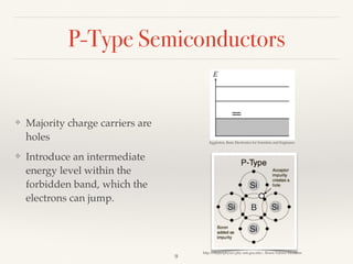
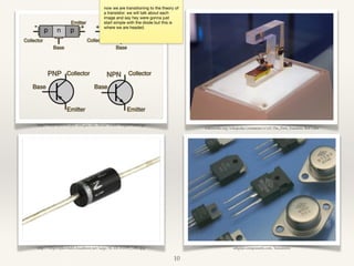
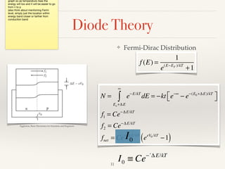
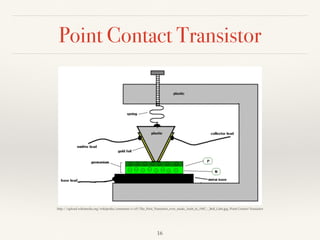
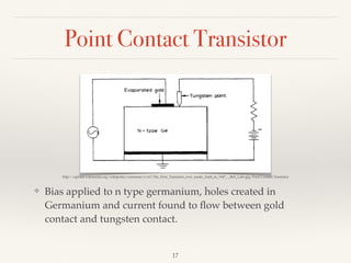
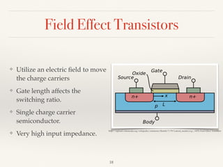
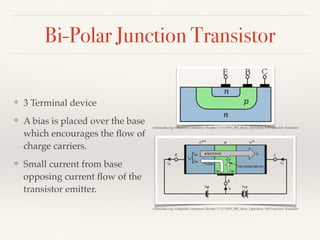
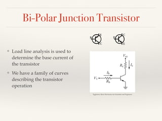
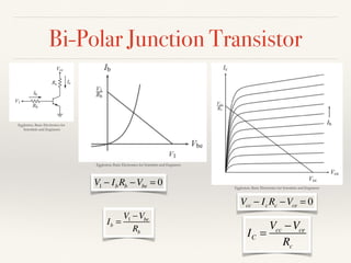
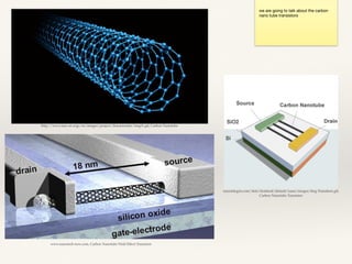
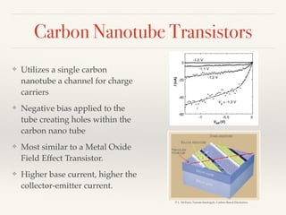
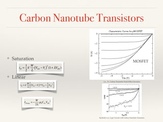
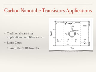
From Glass Tubes to
Carbon Nanotubes
Kevin Kuwata
Monday, March 30, 2015
Department of Physics,
Occidental College
The Transition of the Transistor
1
http://thumbs.dreamstime.com/
Bachtold et al., Science, Logic Circuits with Carbon Nanotube Transistors
Overview
❖ What is a Transistor?
❖ Band Theory
❖ History
❖ Breakthrough Applications
2
What is a Transistor?
❖ Electrical Switch
❖ Signal Amplifier
❖ Voltage Rectifier
❖ Temperature Sensor
3
tandyonline.co.uk, 2n2222
Band Theory of Solids
❖ Discrete energy states in atoms
❖ The Pauli Exclusion Principle
dictates electron shell filling
❖ Bands are the energy states
allowed for an electron
❖ Spacing between the bands
decreases with the addition of
more atoms in a solid.
4
Eggleston, Basic Electronics for Scientists and Engineers
Band Theory cont.
5
❖ Filled energy bands cannot accept electrons.
❖ No electron can be found within the forbidden band.
❖ With sufficient energy, electrons can jump the forbidden band.
Eggleston, Basic Electronics for Scientists and Engineers
Jumping Bands
6
Eggleston, Basic Electronics for Scientists and Engineers
Doping Semiconductors
❖ The process of including impurities in a pure
semiconducting material in hopes to engineer specific
electrical characteristics for a semiconducting material
❖ Increases number of charge carriers present in a
material
❖ P-Type
❖ N-Type
7
N-Type Semiconductors
❖ Majority charge carriers are
negative (electrons)
❖ The dopant introduces
localized energy bands
8
Eggleston, Basic Electronics for Scientists and Engineers
http://hyperphysics.phy-astr.gsu.edu/, Antimony Valence Electrons
P-Type Semiconductors
❖ Majority charge carriers are
holes
❖ Introduce an intermediate
energy level within the
forbidden band, which the
electrons can jump.
http://hyperphysics.phy-astr.gsu.edu/, Boron Valence Electrons
Eggleston, Basic Electronics for Scientists and Engineers
9
now we are transitioning to the theory of
a transistor. we will talk about each
image and say hey were gonna just
start simple with the diode but this is
where we are headed.
sdigital-components.com, Transistors
wikimedia.org/wikipedia/commons/e/e5/The_First_Transisto, Bell Labs
http://d1gsvnjtkwr6dd.cloudfront.net/large/SC-DI-1N5391_LRG.jpg
http://hyperphysics.phy-astr.gsu.edu/hbase/solids/imgsol/tran1.gif
10
Diode Theory
❖ Fermi-Dirac Distribution
f (E) =
1
e(E−EF )/kT
+1
N = e−E/kT
Eo+∆ E
∞
∫ dE = −kt e−∞
− e−(E0 +∆ E)/kT
⎡⎣ ⎤⎦
f1 = Ce−∆ E/kT
f2 = Ce−∆ E/kT
fnet = Ce−´∆ E/kT
eeV0 /kT
−1( )
I0 ≡ Ce−´∆ E/kT
I0
graph so as temperature rises the
energy will too and it will be easier to go
from n to p

(also think about mentioning Fermi
level, simply just the location within
energy band closer or farther from
conduction band

Eggleston, Basic Electronics for Scientists and Engineers
11
V0 − IRL −Vd = 0
Diode Theory
❖ Model the voltage drop over a
diode as 0.6 volts under
forward bias operation.
❖ Kirchhoff Voltage Loop:
I = I0 (eeVd /kT
−1)
Eggleston, Basic Electronics for Scientists and Engineers
http://d1gsvnjtkwr6dd.cloudfront.net/large/SC-DI-1N5391_LRG.jpg
12
V0 − IRL −Vd = 0
Diode Theory
I = I0 (eeVd /kT
−1)
I =
Vo −Vd
RL Leakage Current
Eggleston, Basic Electronics for Scientists and Engineers
figure out a way to link this to
mathematica. may just exit show.
13
NOW we are talking about the top right
picture going to discuss the transistor
inplimentation of third lead, called the
base
sdigital-components.com, Transistors
wikimedia.org/wikipedia/commons/e/e5/The_First_Transisto, Bell Labs
http://d1gsvnjtkwr6dd.cloudfront.net/large/SC-DI-1N5391_LRG.jpg
http://hyperphysics.phy-astr.gsu.edu/hbase/solids/imgsol/tran1.gif
14
Transistors Basics
❖ A transistor is basically a
switch or valve.
❖ Characterized by an IV curve
similar to the diode, but a
family of curves.
❖ Beta
❖ Follow’s Moore’s Law.
wikimedia.org/wikipedia/commons/e/e5/The_First_Transisto, Bell Labs
15
Point Contact Transistor
http://upload.wikimedia.org/wikipedia/commons/e/e5/The_First_Transistor_ever_made,_built_in_1947_-_Bell_Labs.jpg, Point Contact Transistor
16
Point Contact Transistor
❖ Bias applied to n type germanium, holes created in
Germanium and current found to flow between gold
contact and tungsten contact.
17
http://upload.wikimedia.org/wikipedia/commons/e/e5/The_First_Transistor_ever_made,_built_in_1947_-_Bell_Labs.jpg, Point Contact Transistor
Field Effect Transistors
❖ Utilize an electric field to move
the charge carriers
❖ Gate length affects the
switching ratio.
❖ Single charge carrier
semiconductor.
❖ Very high input impedance.
http://upload.wikimedia.org/wikipedia/commons/thumb/7/79/Lateral_mosfet.svg/, NPN Field Effect Transistor
18
Bi-Polar Junction Transistor
❖ 3 Terminal device
❖ A bias is placed over the base
which encourages the flow of
charge carriers.
❖ Small current from base
opposing current flow of the
transistor emitter.
wikimedia.org/wikipedia/commons/thumb/1/13/NPN_BJT_Basic_Operation, NPN junction Transistor
Bi-Polar Junction Transistor
❖ Load line analysis is used to
determine the base current of
the transistor
❖ We have a family of curves
describing the transistor
operation
Eggleston, Basic Electronics for Scientists and Engineers
Bi-Polar Junction Transistor
IC =
Vcc −Vce
Rc
Vcc − IcRc −Vce = 0
Ib =
V1 −Vbe
Rb
V1 − IbRb −Vbe = 0
Eggleston, Basic Electronics for
Scientists and Engineers
Eggleston, Basic Electronics for Scientists and Engineers
www.nanotech-now.com, Carbon Nanotube Field Effect Transistor
we are going to talk about the carbon
nano tube transistors
nanointegris.com/skin/frontend/default/nano/images/Img-Transitors.gif,
Carbon Nanotube Transistor
http://www.tasc-nt.or.jp/en/images/project/characteristic/img01.gif, Carbon Nanotube
Carbon Nanotube Transistors
❖ Utilizes a single carbon
nanotube a channel for charge
carriers
❖ Negative bias applied to the
tube creating holes within the
carbon nano tube
❖ Most similar to a Metal Oxide
Field Effect Transistor.
❖ Higher base current, higher the
collector-emitter current.
P. L. McEuen, Nanotechnologyh, Carbon-Based Electronics
Carbon Nanotube Transistors
❖ Saturation
❖ Linear
iD =
1
2
k'
W
L
VGS −Vt( )2
(1+ λVDS )
iD = k'
W
L
VGS −Vt( )*VDS −
1
2
VDS
2⎡
⎣⎢
⎤
⎦⎥
IDmax = −
W
2L
µ0C0xVDS
2
MOSFET
Bachtold et al., Logic Circuits with Carbon Nanotube Transistors
Liu , X. Carbon Nanotube Field-Effect Inverters
Carbon Nanotube Transistors Applications
❖ Traditional transistor
applications: amplifier, switch
❖ Logic Gates
❖ And, Or, NOR, Inverter
Liu , X. Carbon Nanotube Field-Effect Inverters
Carbon Nanotube Transistors
❖ Hard to place single carbon
nanotubes
❖ Carbon Nanotubes degrade
quickly when exposed to
oxygen
❖ Better flexibility of actual
bonds (flexible electronics)
❖ Heat dissipation
❖ Small temperature
dependence on device
operation
❖ Smaller electronic devices,
easily scalable
❖ Some predict it will help re-
establish Moore’s Law.
Q & A

Comps #2

  • 1.
    From Glass Tubesto Carbon Nanotubes Kevin Kuwata Monday, March 30, 2015 Department of Physics, Occidental College The Transition of the Transistor 1 http://thumbs.dreamstime.com/ Bachtold et al., Science, Logic Circuits with Carbon Nanotube Transistors
  • 2.
    Overview ❖ What isa Transistor? ❖ Band Theory ❖ History ❖ Breakthrough Applications 2
  • 3.
    What is aTransistor? ❖ Electrical Switch ❖ Signal Amplifier ❖ Voltage Rectifier ❖ Temperature Sensor 3 tandyonline.co.uk, 2n2222
  • 4.
    Band Theory ofSolids ❖ Discrete energy states in atoms ❖ The Pauli Exclusion Principle dictates electron shell filling ❖ Bands are the energy states allowed for an electron ❖ Spacing between the bands decreases with the addition of more atoms in a solid. 4 Eggleston, Basic Electronics for Scientists and Engineers Eggleston, Basic Electronics for Scientists and Engineers
  • 5.
    Band Theory cont. 5 ❖Filled energy bands cannot accept electrons. ❖ No electron can be found within the forbidden band. ❖ With sufficient energy, electrons can jump the forbidden band. Eggleston, Basic Electronics for Scientists and Engineers
  • 6.
    Jumping Bands 6 Eggleston, BasicElectronics for Scientists and Engineers
  • 7.
    Doping Semiconductors ❖ Theprocess of including impurities in a pure semiconducting material in hopes to engineer specific electrical characteristics for a semiconducting material ❖ Increases number of charge carriers present in a material ❖ P-Type ❖ N-Type 7
  • 8.
    N-Type Semiconductors ❖ Majoritycharge carriers are negative (electrons) ❖ The dopant introduces localized energy bands 8 Eggleston, Basic Electronics for Scientists and Engineers http://hyperphysics.phy-astr.gsu.edu/, Antimony Valence Electrons
  • 9.
    P-Type Semiconductors ❖ Majoritycharge carriers are holes ❖ Introduce an intermediate energy level within the forbidden band, which the electrons can jump. http://hyperphysics.phy-astr.gsu.edu/, Boron Valence Electrons Eggleston, Basic Electronics for Scientists and Engineers 9
  • 10.
    now we aretransitioning to the theory of a transistor. we will talk about each image and say hey were gonna just start simple with the diode but this is where we are headed. sdigital-components.com, Transistors wikimedia.org/wikipedia/commons/e/e5/The_First_Transisto, Bell Labs http://d1gsvnjtkwr6dd.cloudfront.net/large/SC-DI-1N5391_LRG.jpg http://hyperphysics.phy-astr.gsu.edu/hbase/solids/imgsol/tran1.gif 10
  • 11.
    Diode Theory ❖ Fermi-DiracDistribution f (E) = 1 e(E−EF )/kT +1 N = e−E/kT Eo+∆ E ∞ ∫ dE = −kt e−∞ − e−(E0 +∆ E)/kT ⎡⎣ ⎤⎦ f1 = Ce−∆ E/kT f2 = Ce−∆ E/kT fnet = Ce−´∆ E/kT eeV0 /kT −1( ) I0 ≡ Ce−´∆ E/kT I0 graph so as temperature rises the energy will too and it will be easier to go from n to p (also think about mentioning Fermi level, simply just the location within energy band closer or farther from conduction band Eggleston, Basic Electronics for Scientists and Engineers 11
  • 12.
    V0 − IRL−Vd = 0 Diode Theory ❖ Model the voltage drop over a diode as 0.6 volts under forward bias operation. ❖ Kirchhoff Voltage Loop: I = I0 (eeVd /kT −1) Eggleston, Basic Electronics for Scientists and Engineers Eggleston, Basic Electronics for Scientists and Engineers http://d1gsvnjtkwr6dd.cloudfront.net/large/SC-DI-1N5391_LRG.jpg 12
  • 13.
    V0 − IRL−Vd = 0 Diode Theory I = I0 (eeVd /kT −1) I = Vo −Vd RL Leakage Current Eggleston, Basic Electronics for Scientists and Engineers Eggleston, Basic Electronics for Scientists and Engineers figure out a way to link this to mathematica. may just exit show. 13
  • 14.
    NOW we aretalking about the top right picture going to discuss the transistor inplimentation of third lead, called the base sdigital-components.com, Transistors wikimedia.org/wikipedia/commons/e/e5/The_First_Transisto, Bell Labs http://d1gsvnjtkwr6dd.cloudfront.net/large/SC-DI-1N5391_LRG.jpg http://hyperphysics.phy-astr.gsu.edu/hbase/solids/imgsol/tran1.gif 14
  • 15.
    Transistors Basics ❖ Atransistor is basically a switch or valve. ❖ Characterized by an IV curve similar to the diode, but a family of curves. ❖ Beta ❖ Follow’s Moore’s Law. wikimedia.org/wikipedia/commons/e/e5/The_First_Transisto, Bell Labs 15
  • 16.
  • 17.
    Point Contact Transistor ❖Bias applied to n type germanium, holes created in Germanium and current found to flow between gold contact and tungsten contact. 17 http://upload.wikimedia.org/wikipedia/commons/e/e5/The_First_Transistor_ever_made,_built_in_1947_-_Bell_Labs.jpg, Point Contact Transistor
  • 18.
    Field Effect Transistors ❖Utilize an electric field to move the charge carriers ❖ Gate length affects the switching ratio. ❖ Single charge carrier semiconductor. ❖ Very high input impedance. http://upload.wikimedia.org/wikipedia/commons/thumb/7/79/Lateral_mosfet.svg/, NPN Field Effect Transistor 18
  • 19.
    Bi-Polar Junction Transistor ❖3 Terminal device ❖ A bias is placed over the base which encourages the flow of charge carriers. ❖ Small current from base opposing current flow of the transistor emitter. wikimedia.org/wikipedia/commons/thumb/1/13/NPN_BJT_Basic_Operation, NPN junction Transistor wikimedia.org/wikipedia/commons/thumb/1/13/NPN_BJT_Basic_Operation, NPN junction Transistor
  • 20.
    Bi-Polar Junction Transistor ❖Load line analysis is used to determine the base current of the transistor ❖ We have a family of curves describing the transistor operation Eggleston, Basic Electronics for Scientists and Engineers
  • 21.
    Bi-Polar Junction Transistor IC= Vcc −Vce Rc Vcc − IcRc −Vce = 0 Ib = V1 −Vbe Rb V1 − IbRb −Vbe = 0 Eggleston, Basic Electronics for Scientists and Engineers Eggleston, Basic Electronics for Scientists and Engineers Eggleston, Basic Electronics for Scientists and Engineers
  • 22.
    www.nanotech-now.com, Carbon NanotubeField Effect Transistor we are going to talk about the carbon nano tube transistors nanointegris.com/skin/frontend/default/nano/images/Img-Transitors.gif, Carbon Nanotube Transistor http://www.tasc-nt.or.jp/en/images/project/characteristic/img01.gif, Carbon Nanotube
  • 23.
    Carbon Nanotube Transistors ❖Utilizes a single carbon nanotube a channel for charge carriers ❖ Negative bias applied to the tube creating holes within the carbon nano tube ❖ Most similar to a Metal Oxide Field Effect Transistor. ❖ Higher base current, higher the collector-emitter current. P. L. McEuen, Nanotechnologyh, Carbon-Based Electronics
  • 24.
    Carbon Nanotube Transistors ❖Saturation ❖ Linear iD = 1 2 k' W L VGS −Vt( )2 (1+ λVDS ) iD = k' W L VGS −Vt( )*VDS − 1 2 VDS 2⎡ ⎣⎢ ⎤ ⎦⎥ IDmax = − W 2L µ0C0xVDS 2 MOSFET Bachtold et al., Logic Circuits with Carbon Nanotube Transistors Liu , X. Carbon Nanotube Field-Effect Inverters
  • 25.
    Carbon Nanotube TransistorsApplications ❖ Traditional transistor applications: amplifier, switch ❖ Logic Gates ❖ And, Or, NOR, Inverter Liu , X. Carbon Nanotube Field-Effect Inverters
  • 26.
    Carbon Nanotube Transistors ❖Hard to place single carbon nanotubes ❖ Carbon Nanotubes degrade quickly when exposed to oxygen ❖ Better flexibility of actual bonds (flexible electronics) ❖ Heat dissipation ❖ Small temperature dependence on device operation ❖ Smaller electronic devices, easily scalable ❖ Some predict it will help re- establish Moore’s Law.
  • 27.