Bipolar Junction Transistor
Thetransistor was invented by a team of three scientists at Bell Laboratories, USA in 1947.
Although the first transistor was not a bipolar junction device, yet it was the beginning of a
technological revolution that is still continuing in the twenty first century. All of the complex
electronic devices and systems developed or in use today, are an outgrowth of early
developments in semiconductor transistors.
There are two basic types of transistors : (1) the bipolar junction transistor (BJT) and the
field-effect transistor (FET). The bipolar junction transistor is used in two broad areas of
electronics : (1) as a linear amplifier to boost an electrical signal and (2) as an electronic
switch.
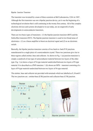
Basically, the bipolar junction transistor consists of two back-to- back P-N junctions
manufactured in a single piece of a semiconductor crystal. These two junctions give rise to
three regions called emitter, base and collector. As shown in Fig. 1 (a) junction transistor is
simply a sandwich of one type of semiconductor material between two layers of the other
type. Fig. 1 (a) shows a layer of N-type material sandwiched between two layers of P-type
material. It is described as a PNP transistor. 1 (b) shown an NPN – transistor consisting of a
layer of P-type material sandwiched between two layers of N-type material.
The emitter, base and collector are provided with terminals which are labelled as E, B and C.
The two junctions are : emitter-base (E/B) junction and collector-base (C/B) junction.
2.
Fig. 1
1. Emitter
Itis more heavily doped than any of the other regions because its main function is to supply
majority charge carries (either electrons or holes) to the base.
2. Base
It forms the middle section of the transistor. It is very thin as compared to either the emitter
or collector and is very lightly-doped.
3. Collector
Its main function (as indicated by its name) is to collect majority charge carriers coming from
the emitter and passing through the base.
Transistor Biasing
For proper working of a transistor, it is essential to apply voltages of correct polarity across
its two junctions. It is worthwhile to remember that for normal operation;
1. emitter-base junction is always forward- biased and
2. collector-base junction is always re- verse-biased.
4.
Summing Up
The fourbasic guideposts about all transistor circuits are :
1. conventional current flows along the arrow whereas electrons flow against it;
2. E/B junction is always forward-biased;
3. C/B junction is always reverse-biased;
4. IE = IB + IC.
Transistor Circuit Configurations
Basically, there are three types of circuit connections (called configurations) for operating a
transistor.
1. common-base (CB), 2. common-emitter (CE), 3. common-collector (CC).
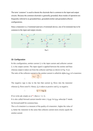
5.
The term ‘common’is used to denote the electrode that is common to the input and output
circuits. Because the common electrode is generally grounded, these modes of operation are
frequently referred to as grounded-base, grounded-emitter and grounded-collector
configurations.
Since a transistor is a 3-terminal (and not a 4-terminal) device, one of its terminals has to be
common to the input and output circuits.
Fig. 4
CB Configuration
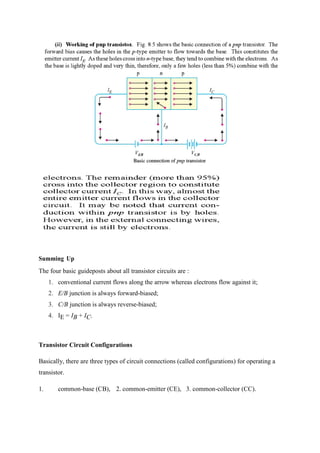
In this configuration, emitter current IE is the input current and collector current
IC is the output current. The input signal is applied between the emitter and base
whereas output is taken out from the collector and base as shown in Fig. 4 (a).
The ratio of the collector current to the emitter current is called dc alpha (dc) of a transistor.
The negative sign is due to the fact that current IE flows into the transistor
whereas IC flows outof it. Hence, IE is taken as positive and IC as negative.
IC = – dc.IE
If we write adc simply as **, then = IC /IE
It is also called forward current transfer ratio (–hFB). In hFB, subscript F stands
for forward andB for common-base.
The of a tranistor is a measure of the quality of a transistor ; higher the value of
, better the transistor in the sense that collector current more closely equals the
emitter current
–IC
dc
IE
6.
CE Configuration
Here, inputsignal is applied between the base and emitter and output signal is
taken out from the collector and emitter circuit. As seen from Fig. 4 (b), IB is the
input current and IC is the output current.
The ratio of the d.c. collector current to dc base current is called dc beta (dc) or just of
the transistor.
= –IC /–IB = IC /IB
or IC = IB
It is also called common-emitter d.c. forward transfer ratio and is written as hFE. It is
possiblefor to have as high a value as 500.
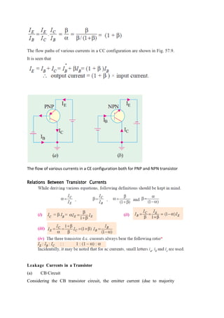
The flow of various currents in a CE configuration both for PNP and NPN transistor is shown
in the figure below. As seen
IE = IB + IC = IB + IB = (1 + ) IB
The flow of various currents in a CE configuration both for PNP and NPN transistor
CC Configuration
In this case, input signal is applied between base and collector and output signal is taken out from emitter-
collector circuit [Fig. 4 (c)]. Conventionally speaking, here IB is the input current and IE is the output current as
shown in Fig. 57.9. The current gain of the circuit is
7.
The flow pathsof various currents in a CC configuration are shown in Fig. 57.9.
It is seen that
The flow of various currents in a CE configuration both for PNP and NPN transistor
Relations Between Transistor Currents
Leakage Currents in a Transistor
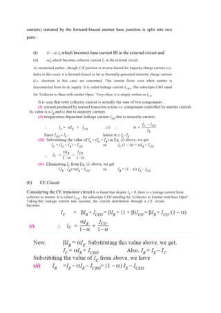
(a) CB Circuit
Considering the CB transistor circuit, the emitter current (due to majority
8.
carriers) initiated bythe forward-biased emitter base junction is split into two
parts :
(i) (1 – ) IE which becomes base current IB in the external circuit and
(ii) IE which becomes collector current IC in the external circuit.
As mentioned earlier , though C/B junction is reverse-biased for majority charge carriers (i.e.
holes in this case), it is forward-biased so far as thermally-generated minority charge carriers
(i.e. electrons in this case) are concerned. This current flows even when emitter is
disconnected from its dc supply. It is called leakage current ICBO. The subscripts CBO stand
for ‘Collector to Base with emitter Open.’ Very often, it is simply written as ICO
(b) CE Circuit
Considering the CE transistor circuit It is found that despite IB = 0, there is a leakage current from
collector to emitter. It is called ICEO , the subscripts CEO standing for ‘Collector to Emitter with base Open’.
Taking this leakage current into account, the current distribution through a CE circuit
becomes
![CE Configuration
Here, input signal is applied between the base and emitter and output signal is
taken out from the collector and emitter circuit. As seen from Fig. 4 (b), IB is the
input current and IC is the output current.
The ratio of the d.c. collector current to dc base current is called dc beta (dc) or just of
the transistor.
= –IC /–IB = IC /IB
or IC = IB
It is also called common-emitter d.c. forward transfer ratio and is written as hFE. It is
possiblefor to have as high a value as 500.
The flow of various currents in a CE configuration both for PNP and NPN transistor is shown
in the figure below. As seen
IE = IB + IC = IB + IB = (1 + ) IB
The flow of various currents in a CE configuration both for PNP and NPN transistor
CC Configuration
In this case, input signal is applied between base and collector and output signal is taken out from emitter-
collector circuit [Fig. 4 (c)]. Conventionally speaking, here IB is the input current and IE is the output current as
shown in Fig. 57.9. The current gain of the circuit is](https://image.slidesharecdn.com/bipolarjunctiontransistorlecturenote092456-250322001120-8f1243a8/85/Bipolar-Junction-Transistor-lecture-note_092456-pdf-6-320.jpg)