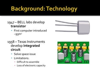
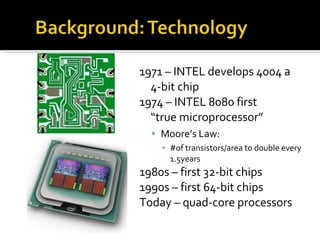
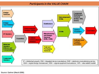
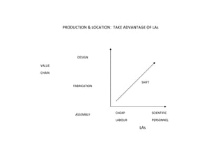
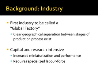
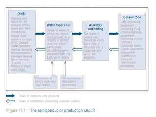
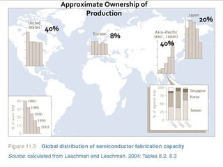
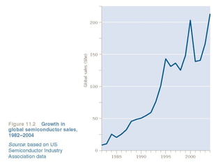
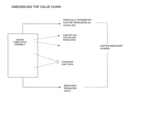
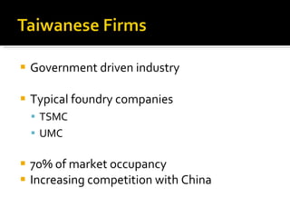
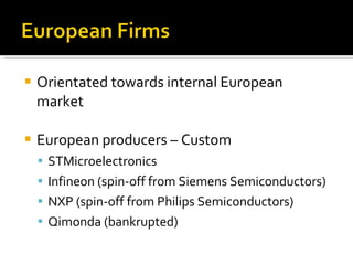
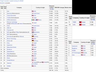
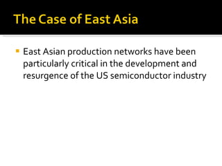
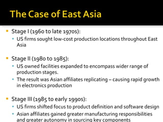
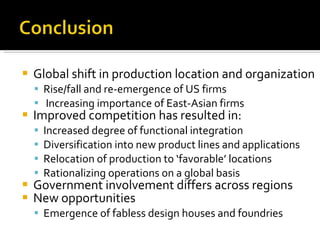
The Global Semiconductor Industry
(Computer Chips)
::TABLE OF CONTENTS::
Overview & Background
Global Shifts & Patterns of Consumption
Production Costs & Technology Development
The Role of the State
Corporate Strategies
Case of East Asia
Discussion
The worldwide semiconductor industry: Trends and opportunities 2016 The Broker Forum
The worldwide semiconductor industry: Trends and opportunities 2016
Today, the rapid pace of innovation and ever-expending use of technologically advanced devices including smartphones, tablets, flat-screen monitors, smart connected cars and medical devices is multiplying the number of semiconductor components being used around us every day. Digitization, connectivity and the internet of things (IOT) now promise solid growth for the global semiconductor market.
Discover how you can develop your business by looking at this market infographic from The Broker Forum.
MicroLED Displays - Market, Industry and Technology Trends 2021Yole Developpement
Strong momentum for MicroLED with progress on all fronts. Cost is the biggest challenge, but Apple and Samsung are carving paths toward the consumer.
More information; https://www.i-micronews.com/products/microled-displays-market-industry-and-technology-trends-2021/
GaAs Wafer and Epiwafer Market: RF, Photonics, LED, Display and PV Applicatio...Yole Developpement
Photonics applications boost the GaAs wafer and epiwafer market with double digit growth.
Learn more about the report here: https://www.i-micronews.com/products/gaas-wafer-and-epiwafer-market-rf-photonics-led-display-and-pv-applications-2020/
Epitaxy Growth Equipment for More Than Moore Devices Technology and Market Tr...Yole Developpement
Driven by microLED displays and power devices, epitaxy equipment shipment volumes will multiply more than threefold over the next five years.
More info on: https://www.i-micronews.com/products/epitaxy-growth-equipment-for-more-than-moore-devices-technology-and-market-trends-2020/
Are you looking to buy Si Wafer? We are a leading supplier of Silicon wafers across six continents in over 45 countries. Call (561) 842-4441 or Shop at our website.
This paper evaluates the diversification opportunities for Indian corporates keen on entering the solar PV manufacturing sector. This includes both crystalline silicon and thin film technologies.
The white paper is divided into three sections. The first section examines the global market dynamics of the solar PV sector and the opportunities and challenges for this sector. This section also provides an introduction to the prominent technologies used in solar PV. Some of the key questions answered in this section include
• What are the global solar PV installation trends?
• Which is the largest solar market in the world?
• What are the various solar PV technologies available?
• What are the key differences between crystalline silicon and thin film technologies?
System-in-Package Technology and Market Trends 2020 report by Yole DéveloppementYole Developpement
How is System-in-Package capably meeting the stringent requirements of consumer applications?
More info here: https://www.i-micronews.com/products/system-in-package-technology-and-market-trends-2020/
Discrete Power Device Packaging: Materials Market and Technology Trends 2019 ...Yole Developpement
Despite the transition to SiP, SoC, and power modules, discrete device packaging still represents a big opportunity especially for materials suppliers.
More information on https://www.i-micronews.com/products/discrete-power-device-packaging-materials-market-and-technology-trends-2019/
Thin wafer processing and Dicing equipment market - 2016 Report by Yole Devel...Yole Developpement
Strong demand for thinner wafers and smaller die is driving the evolution of dicing technologies
Demand for thinned wafers is growing strongly!
Driven by consumer applications such as smartphones, smart cards and stacked packages, the demand for thinned wafers has increased over recent years.
We estimate that the number of thinned wafers used for MEMS devices, CMOS Image Sensors, memory and logic devices, including those with TSVs, as well as and Power devices exceeded the equivalent of 16.5 million 8-inch wafer starts per year (WSPY) in 2015. This is mainly supported by CMOS Image Sensors, followed by Power devices. We expect that this number of thinned wafers will peak at the equivalent of almost 32 million 8-inch WSPY by 2020. This would represent a 14% compound annual growth rate (CAGR) from 2015 to 2020.
Thinner wafers bring several benefits, including enabling very thin packaging, and therefore better form factors, improved electrical performance and high heat dissipation.
Miniaturization towards smaller, higher-performing, lower-cost device configurations has thinned wafers below 100 µm or even 50 µm for some applications, such as memory and power devices.
Forecasts for the number of thinned wafers by thickness and by application are analyzed in this report. It also includes insights on the number of thinning tools, breakdowns by wafer size, and technological highlights affecting the applications mentioned above...
SiC & GaN - Technology & market knowledge updatePntPower.com
Wide Band Gap semiconductor are more and more used in power electronics. Silicon Carbide and Gallium Nitride are now involved in the race to replace silicon. With huge R&D investments and start-ups facing historical players, market and technology knowledge becomes key. Point The Gap presented a SiC & GaN market knowledge update. All the information needed to understand this market, gathered in a few slides by a power electronics market intelligence specialist. Also available on www.PointThePower.com.
Including company names like Transphorm, Infineon, EPC corp., Cambridge electronics, Rohm, Cree, Toyota, Finsix, Zolt, Avogy, etc...
Fan-Out Packaging: Technologies and Market Trends 2019 report by Yole Dévelop...Yole Developpement
Samsung and PTI, with panel-level packaging, have entered the Fan-Out battlefield.
More information on that report at : https://www.i-micronews.com/report/product/fan-out-packaging-technologies-and-market-trends-2019.htm
Status of the Power Electronics Industry 2019 by Yole DéveloppementYole Developpement
Long term growth of the power electronics market is driving 300mm wafer-based production.
More information on: https://www.i-micronews.com/products/status-of-the-power-electronics-industry-2019/
Status of the MEMS Industry 2018 Market and technology Report by Yole Dévelop...Yole Developpement
Megatrends are invigorating the MEMS industry.
More information on : https://www.i-micronews.com/category-listing/product/status-of-the-mems-industry-2018.html
The Semi-Conductor Industry: A Small Guide for Investors & Start- Ups- Semi C...UPE Alliance Group
Since the 1960’s, semiconductor manufacturers in Malaysia have contributed to the production of high-quality semiconductor chips. Malaysian semiconductor manufacturers have supplied some of the world’s largest MNCs from around the world (Germany, US, etc.), including Infineon Technologies, X-Fab and ON Semiconductor. Here is a brief analysis of the Semi Condcutor Industry in Malaysia and it's impact on investors and start ups.
Driven by application diversification, IPDs (integrated passive devices) continue their promising
growth.
Today, miniaturization and integration are key drivers in electronic devices. This is even more critical in several consumer applications, where thinner devices mean higher integration levels, necessitating low-profile components.
More information on that report at http://www.i-micronews.com/reports.html
Detail Project Report (DPR) Li ion assembling unit and Manufacturing SourceAdvisoryServic
Contact at www.sourceadvisory.in for Report. DPR for the Lithium-Ion Manufacturing and assembly unit. Experts in preparation of DPR, Market research Report, Feasibility Report.
Ecosystem Environment for Starting a Semiconductor CompanySteve Szirom
Management presentation on the complex ecosystem necessary for a successful semiconductor startup. Covers key issues: marketing, finacial, legal, PR, funding, and technology.
Lessons for MEMS Test Engineers - Ira Feldman 111020Ira Feldman
Semiconductor Wafer Test Technology and Trends: Lessons for MEMS Test Engineers presentation at MEMS Testing and Reliability 3rd Annual Conference (October 20, 2011) by Ira Feldman (www.hightechbizdev.com)
LED Lighting Market Trends & ON Semiconductor LED Solutions Overview - 1 of 7ON Semiconductor
The LED Lighting revolution is here:
• Global government regulations combined with market forces are the drivers
The opportunity is real and large:
• The retrofit lamps will be the volume driver in the near term
• “Smart Lighting” presents a significant opportunity
ON Semiconductor is well positioned to win with:
• Strong product portfolio
• Complete turn-key solutions
• Breadth of offering
Ultrasonic level sensor Eurosens Dizzi is used for non-contact (non-invasive) level measurement of acoustically transparent liquids. Measurement is done by external echolocation through the bottom of the tank.Innovative design, no tank drilling is required.
This ppt is done by my dear classmate Sap, almost each ppt I have uploaded is copied from net and other sources.I hope this will b a little useful for students..
People looking out for International Trade theories, This Porters Diamond will be a useful presentation for you!... If requested on mail i will send you any particular Topic in International Business.
All the Best!
This was presented by Micheal Khan at the Innovation Festival at Spier Wine Estate on 8 and 9 March 2010. The sponsor was Cape Biotech Trust to raise funds for the Southern African Innovation Network (SAINe).
ITIF Senior Analyst Stephen Ezell presented on the future of advanced manufacturing at the AAAS annual conference. His presentation argued for the correct policies to support a robust advanced manufacturing climate in the United States.
Announcement of interim report by the Information Economy Committee of the Industrial Structure Council
The Information Economy Committee of the Industrial Structure Council (chaired by Mr. Jun Murai, Professor, Fuculty of Environment and Information Studies, Keio University) compiled and released action plans on six priority areas and five cross-sectional policy challenges aiming at the creation of new industries linked to information technologies.
http://www.meti.go.jp/english/press/2011/0811_01.html
GraphRAG is All You need? LLM & Knowledge GraphGuy Korland
Guy Korland, CEO and Co-founder of FalkorDB, will review two articles on the integration of language models with knowledge graphs.
1. Unifying Large Language Models and Knowledge Graphs: A Roadmap.
https://arxiv.org/abs/2306.08302
2. Microsoft Research's GraphRAG paper and a review paper on various uses of knowledge graphs:
https://www.microsoft.com/en-us/research/blog/graphrag-unlocking-llm-discovery-on-narrative-private-data/
Generating a custom Ruby SDK for your web service or Rails API using Smithyg2nightmarescribd
Have you ever wanted a Ruby client API to communicate with your web service? Smithy is a protocol-agnostic language for defining services and SDKs. Smithy Ruby is an implementation of Smithy that generates a Ruby SDK using a Smithy model. In this talk, we will explore Smithy and Smithy Ruby to learn how to generate custom feature-rich SDKs that can communicate with any web service, such as a Rails JSON API.
Encryption in Microsoft 365 - ExpertsLive Netherlands 2024Albert Hoitingh
In this session I delve into the encryption technology used in Microsoft 365 and Microsoft Purview. Including the concepts of Customer Key and Double Key Encryption.
Accelerate your Kubernetes clusters with Varnish CachingThijs Feryn
A presentation about the usage and availability of Varnish on Kubernetes. This talk explores the capabilities of Varnish caching and shows how to use the Varnish Helm chart to deploy it to Kubernetes.
This presentation was delivered at K8SUG Singapore. See https://feryn.eu/presentations/accelerate-your-kubernetes-clusters-with-varnish-caching-k8sug-singapore-28-2024 for more details.
Smart TV Buyer Insights Survey 2024 by 91mobiles.pdf91mobiles
91mobiles recently conducted a Smart TV Buyer Insights Survey in which we asked over 3,000 respondents about the TV they own, aspects they look at on a new TV, and their TV buying preferences.
State of ICS and IoT Cyber Threat Landscape Report 2024 previewPrayukth K V
The IoT and OT threat landscape report has been prepared by the Threat Research Team at Sectrio using data from Sectrio, cyber threat intelligence farming facilities spread across over 85 cities around the world. In addition, Sectrio also runs AI-based advanced threat and payload engagement facilities that serve as sinks to attract and engage sophisticated threat actors, and newer malware including new variants and latent threats that are at an earlier stage of development.
The latest edition of the OT/ICS and IoT security Threat Landscape Report 2024 also covers:
State of global ICS asset and network exposure
Sectoral targets and attacks as well as the cost of ransom
Global APT activity, AI usage, actor and tactic profiles, and implications
Rise in volumes of AI-powered cyberattacks
Major cyber events in 2024
Malware and malicious payload trends
Cyberattack types and targets
Vulnerability exploit attempts on CVEs
Attacks on counties – USA
Expansion of bot farms – how, where, and why
In-depth analysis of the cyber threat landscape across North America, South America, Europe, APAC, and the Middle East
Why are attacks on smart factories rising?
Cyber risk predictions
Axis of attacks – Europe
Systemic attacks in the Middle East
Download the full report from here:
https://sectrio.com/resources/ot-threat-landscape-reports/sectrio-releases-ot-ics-and-iot-security-threat-landscape-report-2024/
Neuro-symbolic is not enough, we need neuro-*semantic*Frank van Harmelen
Neuro-symbolic (NeSy) AI is on the rise. However, simply machine learning on just any symbolic structure is not sufficient to really harvest the gains of NeSy. These will only be gained when the symbolic structures have an actual semantics. I give an operational definition of semantics as “predictable inference”.
All of this illustrated with link prediction over knowledge graphs, but the argument is general.
Securing your Kubernetes cluster_ a step-by-step guide to success !KatiaHIMEUR1
Today, after several years of existence, an extremely active community and an ultra-dynamic ecosystem, Kubernetes has established itself as the de facto standard in container orchestration. Thanks to a wide range of managed services, it has never been so easy to set up a ready-to-use Kubernetes cluster.
However, this ease of use means that the subject of security in Kubernetes is often left for later, or even neglected. This exposes companies to significant risks.
In this talk, I'll show you step-by-step how to secure your Kubernetes cluster for greater peace of mind and reliability.
UiPath Test Automation using UiPath Test Suite series, part 4DianaGray10
Welcome to UiPath Test Automation using UiPath Test Suite series part 4. In this session, we will cover Test Manager overview along with SAP heatmap.
The UiPath Test Manager overview with SAP heatmap webinar offers a concise yet comprehensive exploration of the role of a Test Manager within SAP environments, coupled with the utilization of heatmaps for effective testing strategies.
Participants will gain insights into the responsibilities, challenges, and best practices associated with test management in SAP projects. Additionally, the webinar delves into the significance of heatmaps as a visual aid for identifying testing priorities, areas of risk, and resource allocation within SAP landscapes. Through this session, attendees can expect to enhance their understanding of test management principles while learning practical approaches to optimize testing processes in SAP environments using heatmap visualization techniques
What will you get from this session?
1. Insights into SAP testing best practices
2. Heatmap utilization for testing
3. Optimization of testing processes
4. Demo
Topics covered:
Execution from the test manager
Orchestrator execution result
Defect reporting
SAP heatmap example with demo
Speaker:
Deepak Rai, Automation Practice Lead, Boundaryless Group and UiPath MVP
Dev Dives: Train smarter, not harder – active learning and UiPath LLMs for do...UiPathCommunity
💥 Speed, accuracy, and scaling – discover the superpowers of GenAI in action with UiPath Document Understanding and Communications Mining™:
See how to accelerate model training and optimize model performance with active learning
Learn about the latest enhancements to out-of-the-box document processing – with little to no training required
Get an exclusive demo of the new family of UiPath LLMs – GenAI models specialized for processing different types of documents and messages
This is a hands-on session specifically designed for automation developers and AI enthusiasts seeking to enhance their knowledge in leveraging the latest intelligent document processing capabilities offered by UiPath.
Speakers:
👨🏫 Andras Palfi, Senior Product Manager, UiPath
👩🏫 Lenka Dulovicova, Product Program Manager, UiPath
7. PRODUCTION & LOCATION: TAKE ADVANTAGE OF LAs VALUE CHAIN DESIGN FABRICATION ASSEMBLY CHEAP LABOUR SCIENTIFIC PERSONNEL LAs SHIFT
8.
9.
10.
11.
12.
13.
14. 40% 8% 40% 20% Approximate Ownership of Production
15.
16.
17.
18.
19.
20.
21.
22.
23. UNBUNDLING THE VALUE CHAIN DESIGN FABRICATION ASSEMBLY FABLESS (US) SPECIALIZED PRODUCERS FOUNDRIES (EAST ASIA) VERTICALLY INTEGRATED CAPTIVE PRODUCERS ( IN-HOUSE USE ) CAPTIVE-MERCHANT (HYBRID) MERCHANT PRODUCER (SALE)
24.
25.
26.
27.
28.
29.
30.
31.
32.
33.
34.
35.
36.
37.
38.
39.
40.
41.
42.
43.
44.
45.
46.
47.
48.
49.
50.
51.
52.
Editor's Notes
In 1947, John Bardeen and Walter Brattain, working at Bell Telephone Laboratories, were trying to understand the nature of the electrons at the interface between a metal and a semiconductor three terminal character of the transistor is what allows us to make an amplifier for electrical signals, like the one in our radio. With the three-terminal transistor we can also make an electric switch, which can be controlled by another electrical switch. By cascading these switches (switches that control switches that control switches, etc.) we can build up very complicated logic circuits. These logic circuits can be built very compact on a silicon chip with 1,000,000 transistors per square centimeter. We can turn them on and off very rapidly by switching every 0.000000001 seconds. Such logic chips are at the heart of your personal computer and many other gadgets you use today. In the late 1940‘s, big computers were built with over 10,000 vacuum tubes and occupied over 93 square meters of space. In 1958 and 1959, Jack Kilby at Texas Instruments and Robert Noyce at Fairchild Camera, came up with a solution to the problem of large numbers of components, and the integrated circuit was developed. Instead of making transistors one-by-one, several transistors could be made at the same time, on the same piece of semiconductor. Not only transistors, but other electric components such as resistors, capacitors and diodes could be made by the same process with the same materials. .
For more than 30 years, since the 1960's, the number of transistors per unit area has been doubling every 1.5 years. This fantastic progression of circuit fabrication is known as Moore's law, after Gordon Moore, one of the early integrated circuit pioneers and founders of Intel Corporation mostly the pure elements silicon (Si) and sometimes germanium (Ge) are being used Silicon is a grey colored element with crystalline structure. It is the second most abundant element in the earth's crust, after oxygen. Silicon is always found in combined form in nature, often with oxygen as quartz, and is found in rocks and silica sand http://nobelprize.org/educational_games/physics/transistor/history/
Korea/Taiwan emerge through 1980s/90s,
Much less widespread compared to other industries (ie: automobiles) TODAY approx. ownership of production: **overlap in manufacturing facilities Asia-Pacific – 40% USA – 40% Japan – 20% Europe – 8%
INVISIBLE:: Most people don’t shop for them Importance of military stimulation to industry Japan and Europe, military is less important – demand stimulated by consumer segment new firms that had entered the personal computer market since the second half of the 1970s—Computer, Radio Shack, and Commodore first, and a stream of new start ups later—were all specialized computer firms. These firms preferred to buy advanced semiconductor devices from large capable and innovative microprocessor firms, rather than try to vertically integrate. Thus, Intel became the de-facto leader for the microprocessor market. Communications equipment Internet, mobile phones Digital consumer goods TV, Cameras, Music, PDAs, Video games, etc.
Evident correlation between computer sales and semiconductor suppliers With greater sales to communications equipment suppliers – demand is also connected to NETWORK SERVICE PROVIDERS
New generation effect = as new semi-conductors are produced that are faster and smaller which in turn drops demand for older generations More competitors, with differing operating environments
$200B semiconductor industry generates over $1,200B in electronics systems business and $5,000 billion in services, representing close to 10% of world GDP
In 2005, the semiconductor industry made over 90 million transistors for every man, woman and child on Earth, and by 2010, this number should be 1 billion transistors. Global sales of semiconductors fell 2.8 per cent in 2008 compared with the previous year, the first year-on-year drop since 2001, the Semiconductor Industry Association (SIA) reported on Monday. China – 20%/year growth $42billion to be purchased from chinese designed manufacture
Silverthorne" processor for ultramobile devices Intel's new chip is a tiny 25mm 2 . At only 47 million transistors (about 40 percent of that is a 512K, 8-way set associative L2 cache), it's also quite lean
3 ways for gov’t to help develop industry: 1. Building indigenous production capacity based upon domestically owned firms 2. Attracting foreign semiconductor firms to establish production units 3. Purchasing semi conductors on the open market and contracting on developing the end uses Choice depends on government’s abilities and situation
US-Japan Semiconductor Trade Agreement 1986: allowed American semiconductor manufacturers access to the Japanese market US attempts to solve issue of illegal subsidization of Hynix semiconductors out of Korea has been unsuccessful US attempts to gain fair access to Chinese market also unresolved
VSLI = Very Large Scale Integration
Planning and coordinating semiconductor R&D, import assimilating, disseminating foreign technologies, providing technical assistance to Korean firms and undertaking market research Invariably it was governments, rather than markets, that kick-started the move into chip-making. In some countries, such as Taiwan, the involvement was direct and temporary: both TSMC and UMC were spun off from government-funded research projects into publicly listed companies. In other cases, the involvement was indirect and open-ended: in South Korea, for instance, the government leaned--and continues to lean--on commercial banks to finance the move into chip making by the country's family-controlled conglomerates. The benefits for economic development seemed to justify this approach, and Singapore and Malaysia, too, accepted the idea without question. Source Citation: &quot;The great chip glut; Semiconductor manufacturers.&quot; The Economist (US) (August 11, 2001): N/A. Academic OneFile . Gale. University of Lethbridge. 6 Feb. 2009 <http://0-find.galegroup.com.darius.uleth.ca/itx/start.do?prodId=AONE>. Gale Document Number: A78563321
Taiwanese government has instigated mainly joint-venture spin-off projects by combining local firms with foreign firms and investment Hsinchu Science-Based Industrial Park near Taipei, AKA “silicon valley of the east” Taiwan is now that world’s 3 rd largest semiconductor producer
Almost all firms are foreign, their continued presence proves the kind of supportive environment provided by the government
An integrated device manufacturer (IDM) is a semiconductor company which designs, manufactures, and sells integrated circuit (IC) products. Cypress Semiconductor, Fujitsu, Hitachi, IBM, IDT, Intel, LSI Corporation, Matsushita, Mitsubishi, Freescale, NEC, Philips, NXP, Samsung, STMicroelectronics, Infineon, Sony, National Semiconductor, Texas Instruments, and Toshiba. Vertical integrated captive producers manufacture for in-house use. Vertical integrated captive-merchant producers manufacture semiconductors partly for their own use and partly for sale. Merchant producers are companies making semiconductors only for sale. A fabless semiconductor company specializes in the design and sale of hardware devices implemented on semiconductor chips but do not manufacture them. Nvidia Today most major IDMs including Freescale, Infineon, Texas Instruments and Cypress Semiconductor have adopted the practice of outsourcing chip manufacturing as a significant manufacturing strategy. Foundries manufacture semiconductors to customer specifications but do not design them UMC (United Microelectronics Corporation) which was founded as Taiwan's first semiconductor company in 1980 Taiwan Semiconductor Manufacturing Company (TSMC)
The commercial production of semiconductors began in the U.S. in the 1950s. US firms dominated world semiconductor market for almost three decades until Japanese firms entered to the market and overtaken US firms. Most semiconductor companies, especially IDMs, focused on producing DRAMs, because they could take advantages of mass production to dominate semiconductor market. US firms were overtaken by Japanese firms which entered market with low price and high quality. To recover their market dominance, they had to move our DRAM market into more sophisticated semiconductor devices. Wintelism helped intel positioned in the top semiconductor companies. From that point, U.S. firms settled downed as merchant producer selling semiconductor devices to end users. Although most of US plants are located within the US, they also moved their factories to abroad. Since the early 1960s, US firms have started built assembly plants in Asian country seeking low-labor cost. Fairchild was the first case. In 1962, they build the first plant in HK, and in 1964, General Instruments transferred assembly line to Taiwan. The model has been further validated by the conversion of major IDMs to a completely fabless model, including (for example) Conexant Systems, Semtech, and most recently, LSI Logic.
VLSI project (Very Large Scale Integration) NEC, Fujitsu, Hitachi, Toshiba ,Mitsubishi Japanese government funded 40% of total cost between 1976 and 1979. As us firms did, Japanese firms concentrate on DRAM producing to take advantages of mass production. Japanese firms are typical vertical integrated captive producers, producing chips for in-house use. BUT, the lead of Japanese firms didn’t last long. b/c they were squeezed between reviving US firms targeting non memory semiconductors and Korean firms aiming DRAM industry Contrast to the US, Japanese firms tended to remain in the DRAM market. However, They under-estimated the influence Korean companies. Japan overtaken by a Korean company, Samsung. . To over come this trouble, Japanese firms find new strategies. In 1987, Toshiba invented NAND flash memory, and they diversified their production in flash memory sector. But, it also was overtaken by Samsung in a decade. second solution was increase of outsourcing to reduce the producing cost, which oppose Japanese strategy that keeping their production in-house to control quality Third one was massive merges and joint ventures. In 2002, Mitsubishi and Hitachi were spun off and merged to form a new separate legal entity named Renesas. In 2003, AMD and Fujitsu created a joint-venture company named Spansion.
Like a Japanese semiconductor industry development, Korean government strive to establish a semiconductor industry. Korean government supported 3 major companies, Samsung, LG, and hyundai which are hynix today. Korea also targeted DRAM industry with cheap labor cost, but they invested a huge amount of money on R&D to takeover other developed companies. Korean firms were imitator at the first time. They depended on technology abandoned by US and Japanese firms But their R&D in silicon belly was impressive. Since Samsung invented 64MB DRAM at the first time in 1992, their technology in DRAM manufacturing was ahead of any other company To those firms who rely heavily on a DRAM industry, the rapid decrease of DRAM price is bid damage Due to the decreasing price, Korean firms had to find a breakthrough One was a new target in NAND flash field which was invented by a Japanese firm In 2006, Samsung occupied 48.7% of NAND flash market followed by Toshiba which was 24.6% Recently, Samsung is considering merging the Sandisk, if it happened, it is expected that Samsung solidify their top position in flash memory market The other was diversifying into non-memory market like Application possessors for mobile devices.
Similar to Korea and Japan, there was a intervention of government. Two representative Taiwanese semiconductor companies are state owned companies, which are TSMC (Taiwan Semiconductor Manufacturing Company) and UMC (United Microelectronics Corporation) Joint ventured with qualcomm, solely running two runners In 2006, both companies occupied 70% of foundry market. People question that Chinese SMIC can overtake these two Taiwanese companies Taiwanese experts believe it is not possible Chinese companies could save money on R&D through joint venture with infineon, elpida, toshiba, fujitsu They have only technnique to make memory chips, not logic IC Even though they are willing to invest on R&D, I will be tremendous amount.
STMicroelectronics is an Italian-French electronics and semiconductor manufacturer headquartered in Geneva, Switzerland. On May 1, 2006, Infineon's Memory Products division was carved out as a distinct company called Qimonda AG. In 2006, the semiconductor operations of the parent company, Philips were sold to a consortium of private equity firms through an LBO to form a new separate legal entity named NXP Semiconductors. On May 1, 2006, Infineon's Memory Products division was carved out as a distinct company called Qimonda AG. 2009,JAN,28 Qimonda was bankrupted and impact European silicon Valley
the division of labor between the US and Asia, and within Asia between affiliates and local producers, deepened significantly Now designing and producing
3 ways for gov’t to help develop industry: 1. Building indigenous production capacity based upon domestically owned firms 2. Attracting foreign semiconductor firms to establish production units 3. Purchasing semi conductors on the open market and contracting on developing the end uses