
Recommended
More Related Content
What's hot
What's hot (20)
Similar to ORCAD pcb design
Similar to ORCAD pcb design (20)
More from JHALAKNIHALANI
Recently uploaded
Recently uploaded (20)
ORCAD pcb design
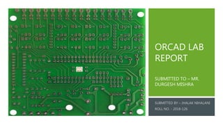
- 1. ORCAD LAB REPORT SUBMITTED TO – MR. DURGESH MISHRA
- 2. WHAT IS ORCAD? OrCAD is a software tool primarily used for electronic design automation(EDA). The software is mainly used by electronic design engineers to create electronic schematics, perform simulations and make prints for manufacturing a PCB. OrCAD Capture - OrCAD Capture is a schematic capture application used for circuit design and PCB editing. editing. Capture doesn’t contain in built simulation feature but exports netlist data to the simulator. It can also export a hardware description of the schematic circuit. EDA - EDA stands for Electronic Design Automation or ECAD Electronic Computer Aided Design. It is a category category of software tools used for designing electronic system such as ICs or PCBs.
- 3. SCHEMATIC DIAGRAM Schematic diagram is the graphical representation of a circuit . All the symbols in the library are standard . Schematic diagram of a CE amplifier -
- 4. PCB LAYOUT A PCB stands for Printed Circuit Board. It mechanically supports and electrically connects electronic components using conductive tracks and pads. PCBs can be single sided (one copper layer) , double sided (two copper layer) or multi layered. Components are generally soldered onto the PCB and it can be either through hole or surface mounted. A PCB layout design is transferred interpretation of schematic diagram. The terms are different between layout and schematic which are shown below- SCHEMAIC DIAGRAM PCB LAYOUT Symbol Footprint Pin Pads Line or Wire Track or Route Drawing connections Routing
- 9. DESIGN RULES AND DESIGN RULE CHECK PCB is the base of electronic products and it is very important to make the PCB with all the rules. Therefore while designing the PCB the designer must create some rules so that the design can effectively solve the functions w.r.t. standard requirements. There are three types of design rules – Electrical Design rules Physical rules Rules of layout versus schematic
- 10. Electrical Design Rules : The electrical path property are important depending on its purpose and type of connection. Some depends the electrical width and the thickness of the path Physical Rules : Mechanical limitations are the factor here as manufacturing maximum height requirement, what type of PCB, amount of components , single or double mounted PCB etc. Rules of Layout versus Schematic: It is important to verify that schematic netlist corresponds to the physical netlist in the layout since missing or extra connections can cause major damage to the design. It is needed to verify if footprint matches physical components.
- 11. HOW TO CREATE A NEW PROJECT From the File menu, choose New, then choose Project. The New Project dialogue box appears. Type a name for your new project in the Name text box. Use the Browse button to select the location. From the File menu, choose New, then choose Design. The design opens in a new PCB project manager and a new schematic page displays. The first time you save a new design, the Save As dialog box appears, giving you the opportunity to specify a drive and replace the system-generated name. HOW TO CREATE A NEW DESIGN
- 12. EXAMPLE : NON INVERTING AMPLIFIER STEPS In the right most tool bar select place part , in the libraries select add library press Ctrl+A and select all the libraries. Now in the search bar type LM741 select the opam Now search R and place 2 resistor, give them value 1K and 10K All the components will be added with .OBL extension Press R to rotate Now connect the wires according to the diagram. For connecting wire press W
- 13. HOW TO DRAW A NEW COMPONENT Select File , then New , in new choose Library A dialogue box will appear select new project , OK Right click on the library , select new part A dialogue box will appear write the name of the component as 555IC Part reference prefix LM555, click OK A new library page will open
- 14. HOW TO DRAW A NEW COMPONENT Now turn the snap to grid on Place > Rectangle draw the body of IC Place > Pins. Enter the name and number of pin Once the component is made, right click on the library Save As, choose the location and Save Now again open schematic page , place part>add library choose the library you made, select the component
- 15. HIGH PASS RC FILTER:
- 16. HOW TO GENERATE BILL OF MATERIAL A bill of materials (BOM) is a centralized source of information used to manufacture a product. It is a list of the items needed to create a product as well as the instructions on how to assemble that product.After the placement of all the components Tools > bill of materials Dialogue box will appear, choose the location Select open to excel if required click OK Design.bom will appear in PCB> output BOM will open, containing information like date, time, Item, Quantity and Reference Part.
- 17. HOW TO GENERATE NETLIST: Netlist gives information about the nets of the circuit . A netlist is simply a list of the electrical connections that describe a circuit ,every component connected to each other have with different nets. It will be a random number . Every net has a unique number .components have net too. Draw the schematic drawing. To assign footprints to the components right click .dsn file > edit object properties Enter the required footprints Now select tools > create netlist Dialogue box will appear, choose the location and click OK
- 18. DESIGN RULE CHECK (DRC) A design rule check (DRC) is simply a set of rules a designer can use to ensure their schematic matches all the dimensional tolerances and manufacturing considerations they set for a board. Select PCB > design rule check Design rule check dialogue box will appear Run If there is no error no green circle will appear But green circle will appear showing error in the circuit
- 19. PCB DESIGN After performing DRC > open PCB editor Setup > design parameter > select grid > OK Now Place > manually A dialogue box will appear which will show all the components of circuit required for designing the PCB All the components will be in components by refdes , select all the components NOTE: as the components were not visible in dialogue box we cannot continue to make the PCB.
- 20. FILE EXTENSIONS FOR ORCAD .OPJ:- project .DSN :- design .DBK :- backup .OLB :- symbol library .UPD :- property update file .DRC :- design rule check .BOM :-bill of materials .EXP :- property export file .MLN :-layout netlist .SWP :-layout back annotation .VHD/.VHO VHDL :-source .EDF / .EDN EDIF :- netlist or back annotation .X.RF :- cross reference .NET :-other netlist
- 21. SOME IMPORTANT UNIT FOR PCB DESIGN 1 mil = 0.001 inch 1 mil = 0.0254mm 1 mm =0.0393 inch 1 mm =39.37mil 1 inch =1000mil
- 22. TYPES OF PCB Single-sided PCB: has a single conductive copper layer above the substrate. The electrical components are soldered or placed on one side of the board. Double-sided PCB: A thin layer of conducting material, such as copper, is added to both the top and bottom sides of the board. Holes in the circuit board allow metal parts to be connected from one side to the other. Multilayer PCB: Multilayer PCBs have more than two copper layers. Multilayer PCBs are designed in a ‘sandwich’ fashion, with several double-sided conductive layers divided by an equal number of insulating material sheets.
- 23. VIA A VIA hole in a PCB consist of two pads in corresponding positions on different layers of the board, that are electrically connected by a hole through the board. The hole is made conducive by electroplating. Types of VIAs Through-hole vias The whole penetrates from the top layer to the bottom layer. They can be either PTH or NPTH. For the PTH the bottom connection is established from the top to the bottom layer. Blind vias The hole penetrates from an exterior layer and ends at an interior layer. Here, the hold doesn’t penetrate through the entire board but connect the PCB’s exterior layer to add one interior layer. Either connection is from the top layer to a layer in the centre or from the bottom layer to some layer in the interior region. The other end of the hole cannot be seen once the lamination is done. Hence, they are called blind vias
- 24. SILK SCREEN: Let’s start with an ordinary bare-bones circuit select the top copper layer and draw text, pad, and traces if you etch the board at home, the element will have a similar look of the image below. Notice that text, pads, and traces are all made out of the same material (copper). They all have a reddish brown metallic color. In your layout program, you can place the text and part outlines on the silk screen layer instead of copper. In the photo below, see how to text and part outlines are now a different color than the traces and pads. The silk screen layer is just ink. The ink is non-conductive add can be placed on top of traces without interference.
- 25. SILK SCREEN: Besides making better use of board space the silkscreen layer is brighter, providing better contrast for faster hand assembly. part outlines indicates part orientation, and makes it obvious when you’ve forgotten to insert a part. below is an example of different silkscreen appearance of a part outline, as produced by various manufacturers.
- 26. SOLDER MASK Solder mask is a thin layer of polymer that is usually applied to the copper traces of the PCB for protection against oxidation, add prevent solder bridges from forming around or between solder pads. A solder bridge is an unintended electrical connection between the 2 conductors with a small blob of solder, and the boards can prevent this from happening with solder masks.
- 27. THERMAL RELIEF Thermal relief is a technique used by print circuit board(PCB) designer to thermally the couple soldering pads from large copper areas in order to avoid excessive heat transfer from the pads during the soldering process, which would result in late melting or even no melting at all of the soldering alloy
- 28. ANTIPAD The end the pad is the void area (shown as the blue annular ring in diagram below) between the pad and a copper of the plane. It should be designed so that it maintains the impedance of a transmission line as it passes through the plane.
- 29. GERBER FILE Gerber files are files of PCB fabrication data that we provide to manufacturer containing information regarding PCB Components like copper traces, drill holes, etc. instead of sending actual PCB design file to manufacturer. The Gerber format is an open ASCII vector format for printed circuit board designs. It is the de facto standard used by PCB industry software to describe the printed circuit board images: copper layers, solder mask, legend, drill data, etc.
- 30. NC DRILL FILE NC drill file(numeric control drill file), refers to a file regulating all the information concerning hole or via drilling requirement including tooling size, hole size and location. It’s important for PCB design engineers to create NC drill files since a lot of trouble can be avoided when PCB files are converted into NC drill files and Gerber files.
- 31. THANKYOU