SlideShare a Scribd company logo
1 of 17
Download to read offline
IOSR Journal of Electrical and Electronics Engineering (IOSR-JEEE)
e-ISSN: 2278-1676,p-ISSN: 2320-3331, Volume 10, Issue 4 Ver. II (July – Aug. 2015), PP 01-17
www.iosrjournals.org
DOI: 10.9790/1676-10420117 www.iosrjournals.org 1 | Page
Study and Design, Simulation of PWM based Buck converter for
Low Power Application
Mr. Sanjay Murmu, Mr.SSPM Sharma B
M.Tech Student,
Department of Electrical Engineering, Mewar University Chittorgarh(Raj) 312901
Asst.Proff, Department of Electrical Engineering, Mewar University Chittorgarh(Raj) 312901
Abstract: Now a day’s dc-dc switching converters are widely used for sophisticated application. By using these
converters with given dc input voltage a stabilised output voltage can be obtained by using Buck (lower), Boost
(higher) or Buck –Boost (generic) topology which improves the efficiency of dc-dc converter as compared to
linear regulators. Most used technique to control switching power supply is pulse width modulation (PWM). In
this way a particular dc-dc converter is designed by keeping the typical application in mind. A properly
designed dc-dc converter provide low ripple, better noise rejection, reliable and efficient converter. For some
typical application like powering LED needs constant current supply for constant illumination, hence feedback
based closed loop converters becomes better choice. In the present thesis for low power application a PWM
based closed loop dc-dc buck converter has been designed, analysed and simulated. A MOSEFET has been used
as switching device and components has been designed for low ripple and low noise. With variation in load and
variation in input power supply output supply voltage has been obtained as constant value by using PID
controller. The performance of PID controller and switching frequency has been adjusted such that the output
voltage maintain at 8 V. By rigorous simulation procedure it has been obtained that for load resistance in the
range of 10Ω to 35Ω and with the value of P = 8, I = 20 and at a switching frequency of 100 KHz, the output
voltage provides a constant value at 7.995 V approximately. The maximum ripple value obtained is 4%.
MATLAB has been used as a tool for simulation. The performance of converter has been analysed by
controlling PID controller.
Keyword: - Linear Regulator, Switching Regulator, Ripple/Noise, Converter, transistor switch, capacitor,
diode, inductor, pulse-width modulating controller etc.
I. Introduction
Linear regulators are great for powering very low powered devices. They are easy to use and cheap,
and therefore are very popular. However, due to the way they work, they are extremely inefficient.
A linear regulator works by taking the difference between the input and output voltages, and just
burning it up as waste heat. The larger the difference between the input and output voltage, the more heat is
produced. In most cases, a linear regulator wastes more power stepping down the voltage than it actually ends
up delivering to the target device. With typical efficiencies of 40%, and reaching as low as 14%, linear voltage
regulation generates a lot of waste heat which must be dissipated with bulky and expensive heat sinks. This also
means reduced battery life for your projects. A switching regulator works by taking small chunks of energy, bit
by bit, from the input voltage source, and moving them to the output. This is accomplished with the help of an
electrical switch and a controller which regulates the rate at which energy is transferred to the output. The
energy losses involved in moving chunks of energy around in this way are relatively small, and the result is that
a switching regulator can typically have 85% efficiency. Since their efficiency is less dependent on input
voltage, they can power useful loads from higher voltage sources.
Linear Regulator
Study and Design, Simulation of PWM basedBuck converter for Low Power Application
DOI: 10.9790/1676-10420117 www.iosrjournals.org 2 | Page
A simple Linear Regulator. If we consider an example, where Vin= 12V and we want to have a Vout=
8V. In this case we need to drop 4 volts across the regulator.
Using standard power equation: P = V*I
If the output current = 10A, this will result in 10 A * 4 V = 40 W.
Now the regulator must dissipate 40 W of heat energy. This results in a mere 66.6% efficiency for the
linear regulator and a lot of wasted power which is normally transformed into heat. Provision for heat sinks for
cooling makes the regulator bulky and large. Hence, where size and efficiency are critical, linear voltage
regulators cannot be used.
Figure 2 is a very basic switching regulator. The switching regulator is a simple switch (and hence
ideally no resistance or very low resistance). This switch goes on and off at a fixed rate (usually between 50
KHz to 100 KHz) as show
Switching Regulator
The Duty Cycle for the switch is determined by the Eq.
Duty Cycle =
Vout
Vin
The time that the switch remains closed during each switch cycle is varied to maintain a constant
output voltage. The switching regulator is much more efficient than the linear regulator achieving efficiencies as
high as 80% to 95% in some circuits. In contrast, the linear regulator usually exhibits only 50% to 60%
efficiency. With higher efficiency smaller heat sinks will be required because lesser heat is dissipated.
Comparison between Linear Regulator and Switching Regulator
Linear Switching
Function Only step down; input voltage must be
greater than output.
Step up, Step down, or inverts
Complexity Low, which usually requires only the
regulator and low value bypass capacitors.
Medium to high, which usually requires
inductor, diode, an filter caps in addition
to the IC; for high power circuits, external
FFTs are needed
Ripple/Noise Low; no ripple, better noise rejection. Medium to high, due to ripple at switching
rate.
Efficiency Low to medium, But actual battery life
depends on load current and battery
voltage over time; high if Vin-Vout
difference is small.
High, except at very low load
currents(µA), where switch mode
quiescent current is usually higher
Size Small to medium in portable designs, but
may be larger if heat sinking is needed
Larger than linear at low power, but
smaller at power levels for which linear
requires a heat sink.
Total cost Low Medium to high, largely due to external
components.
Waste heat High, if average load and/or input/output
voltage difference are high.
Low as components usually run cool for
power levels below 12W
DC-DC Converter
DC-DC converters are electronic devices that are used whenever we want to change DC electrical
power efficiently from one voltage level to another. In the previous chapter we mentioned the drawbacks of
doing this with a linear regulator.
Types of Converters
Currently, dc/dc converters can be divided into two broad categories:
• Non-isolated dc/dc converters
• Isolated dc/dc converters
Study and Design, Simulation of PWM basedBuck converter for Low Power Application
DOI: 10.9790/1676-10420117 www.iosrjournals.org 3 | Page
Non-Isolated DC/DC Converters
The non-isolated converter usually employs an inductor, and there is no dc voltage isolation between
the input and the output. The vast majority of applications do not require dc isolation between input and output
voltages. The non-isolated dc-dc converter has a dc path between its input and output. Battery-based systems
that don’t use the ac power line represent a major application for non-isolated dc-dc converters. Point-of-load
dc-dc converters that draw input power from an isolated dc-dc converter, such as a bus converter, represent
another widely used non-isolated application. Most of these dc-dc converter ICs use either an internal or
external synchronous rectifier. Their only magnetic component is usually an output inductor and thus less
susceptible to generating electromagnetic interference. For the same power and voltage levels, it usually has
lower cost and fewer components while requiring less pc-board area than an isolated dc-dc converter. For lower
voltages (12V) non-isolated buck converters can be used.
Isolated DC/DC Converters
For safety considerations, there must be isolation between an electronic system’s ac input and dc
output. Isolation requirements cover all systems operating from the ac power line, which can include an isolated
front-end ac-dc power supply followed by an isolated “brick” dc-dc converter, followed by a non-isolated point-
of-load converter. Typical isolation voltages for ac-dc and dc-dc power supplies run from 1500 to 4000V,
depending on the application. An isolated converter employs a transformer to provide dc isolation between the
input and output voltage which eliminates the dc path between the two.
Isolated dc-dc converters use a switching transformer whose secondary is either diode-or synchronous-
rectified to produce a dc output voltage using an inductor capacitor output filter. This configuration has the
advantage of producing multiple output voltages by adding secondary transformer windings. For higher input
voltages (48V) transformer isolated converters are more viable
Buck Converter – Theory of Operation
The name “Buck Converter” presumably evolves from the fact that the input voltage is
bucked/chopped or attenuated, in amplitude and a lower amplitude voltage appears at the output. A buck
converter, or step-down voltage regulator, provides non-isolated, switch-mode dc-dc conversion with the
advantages of simplicity and low cost. Figure 3 shows a simplified non-isolated buck converter that accepts a dc
input and uses pulse-width modulation (PWM) of switching frequency to control the output of an internal power
MOSFET. An external diode, together with external inductor and output capacitor, produces the regulated dc
output.
.
Non isolated Buck Regulator
The buck converter here onwards is introduced using the evolutionary approach. Let us consider the
circuit in Figure 4(a), containing a single pole double-throw switch.
Study and Design, Simulation of PWM basedBuck converter for Low Power Application
DOI: 10.9790/1676-10420117 www.iosrjournals.org 4 | Page
Buck Converter
The output voltage equals the input voltage when the switch is in position 1 and it is zero when the
switch is in position 2. By varying the duration for which the switch is in position 1 and 2, it can be seen that the
average output voltage can be varied, but the output voltage is not pure dc. The circuit in (a) can be modified as
shown in belwo by adding an inductor in series with the load resistor. An inductor reduces ripple in current
passing through it and the output voltage would contain less ripple content since the current through the load
resistor is the same as that of the inductor. When the switch is in position A, the current through the inductor
increases and the energy stored in the inductor increases. When the switch is in position 2, the inductor acts as a
source and maintains the current through the load resistor. During this period, the energy stored in the inductor
decreases and its current falls. It is important to note that there is continuous conduction through the load for this
circuit. If the time constant due to the inductor and load resistor is relatively large compared with the period for
which the switch is in position 1 or 2, then the rise and fall of current through inductor is more or less linear, as
shown in Figure 5.
Effect of an Inductor
A capacitor reduces the ripple content in voltage across it, whereas an inductor smoothes the current
passing through it. The combined action of LC filter reduces the ripple in output to a very low level.
Circuit with an LC Filter
With the circuit in Figurer it is possible to have a power semiconductor switch to correspond to the
switch in position 1 and a diode in position 2. The circuit that results is shown in Figure 7. When the switch is in
position 2, the current will pass through the diode. The important thing now is the controlling of the power
semiconductor switch.
Study and Design, Simulation of PWM basedBuck converter for Low Power Application
DOI: 10.9790/1676-10420117 www.iosrjournals.org 5 | Page
Buck converter without feedback
The circuit in Figure Bulk converter without feedback can be regarded as the most elementary buck
converter without a feedback. The Buck Converter transfers small packets of energy with the help of a power
switch, a diode, and an inductor and is accompanied by an output filter capacitor and input filter. All the other
topologies such as the Boost, Buck-Boost Converter etc, vary by the different arrangement of these basic
components.
This circuit can be further modified by adding the feedback part which is integral for a stabilizes the
output. Such a circuit is shown in the Figurers below.
Step down Buck Converter with feedback
The PWM Controller above figure compares a portion of the rectified dc output with a voltage
reference (Vref) and varies the PWM duty cycle to maintain a constant dc output voltage. If the output voltage
wants to increase, the PWM lowers its duty cycle to reduce the regulated output, keeping it at its proper voltage
level. Conversely, if the output voltage tends to go down, the feedback causes the PWM duty cycle to increase
and maintain the proper output. A buck converter or step-down switch mode power supply can also be called a
switch mode regulator
Different components in the Buck Converter
Buck converter consists of five standard components:
 transistor switch (active switch)
 capacitor
 diode (passive switch)
 inductor
 pulse-width modulating controller
Switch
In its crudest form a switch can be a toggle switch which switches between supply voltage and ground.
But for all practical applications which we shall consider we will deal with transistors. Transistors chosen for
use in switching power supplies must have fast switching times and should be able to withstand the voltage
spikes produced by the inductor. The input on the gate of the transistor is normally a Pulse Width Modulated
(PWM) signal which will determine the ON and OFF time. Sizing of the power switch is determined by the load
current and off-state voltage capability.
Operating Frequency
The operating frequency determines the performance of the switch. Switching frequency selection is
typically determined by efficiency requirements. There is now a growing trend in research work and new power
supply designs in increasing the switching frequencies. The higher is the switching frequency, the smaller the
physical size and component value. The reason for this is to reduce even further the overall size of the power
supply in line with miniaturisation trends in electronic and computer systems.
Capacitor
Capacitor provides the filtering action by providing a path for the harmonic currents away from the
load. Output capacitance (across the load) is required to minimize the voltage overshoot and ripple present at the
output of a step-down converter. The capacitor is large enough so that its voltage does not have any noticeable
change during the time the switch is off. Large overshoots are caused by insufficient output capacitance, and
Study and Design, Simulation of PWM basedBuck converter for Low Power Application
DOI: 10.9790/1676-10420117 www.iosrjournals.org 6 | Page
large voltage ripple is caused by insufficient capacitance as well as a high equivalent-series resistance (ESR) in
the output capacitor. The maximum allowed output voltage overshoot and ripple are usually specified at the time
of design. Thus, to meet the ripple specification for a step-down converter circuit, we must include an output
capacitor with ample capacitance and low ESR.
Inductor
The function of the inductor is to limit the current slew rate (limit the current in rush) through the
power switch when the circuit is ON. The current through the inductor cannot change suddenly. When the
current through an inductor tends to fall, the inductor tends to maintain the current by acting as a source. This
limits the otherwise high-peak current that would be limited by the switch resistance alone. The key advantage
is when the inductor is used to drop voltage, it stores energy. Also the inductor controls the percent of the ripple
and determines whether or not the circuit is operating in the continuous mode.
Pulse-width modulating controller
Pulse Width Modulation (PWM)
Design and analysis of Buck Converter
The buck converter is used for step down operation. A buck converter with its output filter area
Open loop buck converter
When the switch S1 is on and S2 is off, the input voltage appears across the inductor and current in
inductor increases linearly. In the same cycle the capacitor is charged. When the switch S1 is on and S2 is off,
the voltage across the inductor is reversed. However, current in the inductor cannot change instantaneously and
the current starts decreasing linearly. In this cycle also the capacitor is also charged with the energy stored in the
inductor.
Continuous Mode / Discontinuous Mode
During the ON state and then the subsequent OFF state the Buck Converter can operate in Continuous
Mode or Discontinuous Mode. The difference between the two is that in CCM the current in the inductor does
not fall to zero.
(a) Continuous mode (b) Discontinuous mode
Study and Design, Simulation of PWM basedBuck converter for Low Power Application
DOI: 10.9790/1676-10420117 www.iosrjournals.org 7 | Page
Calculation for Duty Ratio
For calculation of the duty ratio we will first of all assume that the converter is in steady state. The
switches are treated as being ideal, and the losses in the inductive and the capacitive elements are neglected.
Also it is important to point out that the following analysis does not include any parasitic resistances (all ideal
case). The analysis also has the assumption that the converter is operating in Continuous conduction mode only
i.e. iL(t) > 0.When the switch is on for time duration ton , the switch conducts the inductor current and the diode
becomes reverse biased. This results in a positive voltage vL=Vd-Vo across the inductor in Figure 12 (a). This
voltage causes a linear increase in the inductor current iL. When the switch is turned off, because of the
inductive energy storage, iL continues to flow. This current now flows through the diode, and vL = −Vo in Figure.
Since in steady-state operation waveform must repeat from one time period to the next, the integral of the
inductor voltage L v over one time period must be zero, where Ts = ton+ toff .
𝑣𝐿
𝑇𝑠
0
𝑑𝑡 = 𝑣𝐿
𝑡𝑜𝑛
0
𝑑𝑡 + 𝑣𝐿
𝑇𝑠
𝑡𝑜𝑛
𝑑𝑡 = 0
It implies that areas A and B must be equal. Therefore,
𝑉𝑑 − 𝑉𝑜 𝑡 𝑜𝑛 = 𝑉𝑜 𝑇𝑠 − 𝑡 𝑜𝑛
or
𝑉𝑜
𝑉𝑑
=
𝑡 𝑜𝑛
𝑇𝑠
= 𝐷 𝐷𝑢𝑡𝑦 𝑅𝑎𝑡𝑖𝑜
Hence in this mode, the voltage output varies linearly with the duty ratio of the switch for a given input
voltage and does not depend on any other circuit parameter.
Step down converter circuit states for CCM mode: (a) Switch on; (b) Switch off
Calculation for Inductor
We can derive a simplified differential equation based on the assumption that the voltage across the
load, and thereby across the capacitor, is fairly constant. The differential equation in terms of the current
through the inductor, when the switch is closed, may now be written as
𝐿𝑖 𝐿 𝑡
𝑑𝑡
= 𝑉𝑑 − 𝑉𝑜 − − − − − − − − − − − − − (1)
Assuming that the circuit has assumed steady state hence there may already be some current in the
inductor, ILmin , just prior to the closing of switch S. Hence for a time interval 0 ≤t ≤ Ton = DT , gives:
𝑖 𝐿 𝑡 =
𝑉𝑑 − 𝑉𝑜
𝐿
𝑡 + 𝐼𝐿,𝑚𝑖𝑛 − − − − − − − − − − − −(2)
The inductor current increases linearly with time and attains its maximum value
Il,max as t→TON =DT such that
Study and Design, Simulation of PWM basedBuck converter for Low Power Application
DOI: 10.9790/1676-10420117 www.iosrjournals.org 8 | Page
𝐼𝐿,𝑚𝑎𝑥 =
𝑉𝑑 − 𝑉𝑜
𝐿
𝐷𝑇 + 𝐼𝐿,𝑚𝑖𝑛 − − − − − − − − − − − (3)
Defining the change in the current from its minimum to maximum value as the peak-to-peak current
ripple ΔIL , the equation 4-6 yields an expression for ΔIL ,as
𝛥𝐼𝐿 = 𝐼𝐿,𝑚𝑎𝑥 − 𝐼𝐿,𝑚𝑖𝑛 =
𝑉𝑑 − 𝑉𝑜
𝐿
𝐷𝑇 − − − − − − − − − − − −(4)
Note that the current ripple is directly proportional to D, the duty cycle, upon which we may not have
any control because of the output voltage requirement. However, it is inversely proportional to the inductance L
upon which we can exert some control. Thus, the current ripple can be controlled by a proper selection of the
inductor.
Let us now analyze the circuit when the switch is in its open position. The inductor current completes
its path through the lower side MOSFET and the corresponding differential equation, for OFF 0 ≤ t ≤ TOFF, is
𝐿
𝑑𝑖 𝐿 t
𝑑𝑡
= −𝑉𝑜 − − − − − − − − − − − − − (5)
From the solution of the above first-order differential equation, we obtain
𝑖 𝐿 𝑡 = −
𝑉𝑜
𝐿
𝑡 + 𝐼𝐿,𝑚𝑎𝑥 − − − − − − − − − (6)
Where IL,max is the maximum value of the current in the inductor at the opening of the switch or the
beginning of the off period. As t →Toff = (1−D )T, the inductor current decreases to its minimum value IL,min
such that
𝐼𝐿,𝑚𝑖𝑛 = −
𝑉𝑜
𝐿
1 − 𝐷 𝑇 + 𝐼𝐿,𝑚𝑎𝑥 − − − − − − − −(7)
The Eq. 7 yields another expression for the peak-to-peak current ripple as
∆𝐼𝐿 = 𝐼𝐿,𝑚𝑎𝑥 − 𝐼𝐿,𝑚𝑖𝑛 =
𝑉𝑜
𝐿
1 − 𝐷 𝑇 − − − − − − − −(8)
Inductor Current
The current through the inductor as given by Eq. 2 during the on time and by Eq. 6 during the off time
is sketched in the Figure 13. The average current in the inductor must be equal to the dc current through the
load. That is,
𝐼𝐿,𝑎𝑣𝑔 = 𝐼𝑜 =
𝑉𝑜
𝑅
− − − − − − − −(9)
The expressions for the maximum and minimum currents through the inductor may now be written as
𝐼𝐿,𝑚𝑎𝑥 = 𝐼𝐿,𝑎𝑣𝑔 +
∆𝐼𝐿
2
=
𝑉𝑜
𝑅
+
𝑉𝑜
2𝐿
1 − 𝐷 𝑇 − − − − − − − (10)
𝐼𝐿,𝑚𝑖𝑛 = 𝐼𝐿,𝑎𝑣𝑔 −
∆𝐼𝐿
2
=
𝑉𝑜
𝑅
−
𝑉𝑜
2𝐿
1 − 𝐷 𝑇 − − − − − (11)
The current supplied by the source varies from IL,min to IL,max during the time the switch is closed and
is zero otherwise as shown in Figure 14.
Study and Design, Simulation of PWM basedBuck converter for Low Power Application
DOI: 10.9790/1676-10420117 www.iosrjournals.org 9 | Page
Source Current
When the switch, the inductor, and the capacitor are treated as ideal elements, the average power
dissipated by them is zero. Consequently, the average power supplied by the source must be equal to the average
power delivered to the load. That is,
𝑉𝑑 𝐼 𝑑 = 𝑉𝑜 𝐼𝑜 = 𝐷𝑉𝑠 𝐼𝑠 − − − − − −(12)
This equation helps us express the average source current in terms of the average load current as
𝐼𝑠 = 𝐷𝐼𝑜 the current through the lower side MOSFET is shown in Figure 15. Its average value is
𝐼𝐿𝑠 = 1 − 𝐷 𝐼𝑜 − − − − − − − − 13
Current through low side of Mosefet
We know the fact that the buck converter can either operate in its continuous conduction mode or
discontinuous mode. When it operates in the continuous conduction mode, there is always a current in the
inductor. The minimum current in the continuous conduction mode can be zero. Consequently, there is a
minimum value of the inductor that ensures its continuous conduction mode. It can be obtained from Eq. 11 by
setting IL min to zero as
𝑉𝑜
𝑅
−
𝑉𝑜
2𝐿 𝑚𝑖𝑛
1 − 𝐷 𝑇 = 0 − − − − − − − (14)
Hence,
𝐿 𝑚𝑖𝑛 =
1 − 𝐷
2
𝑅𝑇 =
1 − 𝐷
2𝑓
𝑅 − − − −(15)
Calculation for Capacitor
The output capacitor is assumed to be so large as to yield vo(t)=Vo . However, the ripple in the output
voltage with a practical value of capacitance can be calculated by considering the waveforms shown in Figure
16 for a continuous conduction mode of operation. Assuming that all of the ripple component in iL flows
through the capacitor and its average component flow through the load resistor, the shaded area in Figure 16
represents an additional charge ΔQ.
Output Voltage ripple in a step down Converter
Study and Design, Simulation of PWM basedBuck converter for Low Power Application
DOI: 10.9790/1676-10420117 www.iosrjournals.org 10 | Page
Therefore, the peak-to-peak voltage ripple ∆𝑉𝑜 can be written as
∆𝑉𝑜 =
∆𝑄
𝐶
=
1
𝐶
1
2
𝛻𝐼𝐿
2
𝑇𝑠
2
− − − − − − − − − (16)
From Figure 16 during toff
∆𝐼𝐿 =
𝑉𝑜
𝐿
1 − 𝐷 𝑇𝑠 − − − − − − − −(17)
Therefore, substituting ΔIL from Eq. 17 into the Eq. 16 gives
∆𝑉𝑜 =
𝑇𝑠
8𝐶
𝑉𝑜
𝐿
1 − 𝐷 𝑇𝑠 − − − − − − − (18)
∆𝑉𝑜
𝑉𝑜
=
1
8
𝑇𝑠
2
1 − 𝐷
𝐿𝐶
=
𝜋2
2
1 − 𝐷
𝑓𝑐
𝑓𝑠
2
− − − − − − − (19)
Where switching frequency fs =1/T and
𝑓𝑐 =
1
2𝜋 𝐿𝐶
− − − − − (20)
Equation 19 shows that the voltage ripple can be minimized by selecting a corner frequency fc of the
low pass filter at the output such that fc <<fs. Also, the ripple is independent of the output load power, so long
as the converter operates in the continuous-conduction mode. We should note that in switch-mode dc power
supplies, the percentage ripple in the output voltage are usually specified to be less than, for instance, 1%.
The analysis carried out above assumes ideal components and if we were to make the analysis using all
the non-ideal components it would make the derivation a bit more complex with a lot of other parameters
included in the final equation. But for the calculation of initial values of the components the above
approximations does result in reasonable values. It is also important to realize here that the ESR and ESL are
also important and can even dominate. More about how the non-ideality can affect the overall system can be
found on [6].
PWM Controller
The heart of a switching power supply is its switch control circuit (controller). One of the key
objectives in designing a controller for the power converter is to obtain tight output voltage regulation under
different line and load conditions [7]. Often, the control circuit is a negative-feedback control loop connected to
the switch through a comparator and a Pulse Width Modulator (PWM). The switch control signal (PWM),
controls the state (on or off) of the switch. This control circuit regulates the output voltage against changes in
the load and the Input voltage.
PWM
PWM is the method of choice to control modern power electronics circuits. The basic idea is to control
the duty cycle of a switch such that a load sees a controllable average voltage. To achieve this, the switching
frequency (repetition frequency for the PWM signal) is chosen high enough that the load cannot follow the
individual switching events and they appear just a “blur” to the load, which reacts only to the average state of
the switch.
With pulse-width modulation control, the regulation of output voltage is achieved by varying the duty
cycle of the switch, keeping the frequency of operation constant. Duty cycle refers to the ratio of the period for
which the power semiconductor is kept ON to the cycle period.
Study and Design, Simulation of PWM basedBuck converter for Low Power Application
DOI: 10.9790/1676-10420117 www.iosrjournals.org 11 | Page
Comparator and Voltage to PWM Converter
Switching power supplies rely on negative feedback to maintain the output voltages at their specified
value. To accomplish this, a differential amplifier is used to sense the difference between an ideal voltage (the
reference voltage) and the actual output voltage to establish a small error signal (v control).
Voltage Reference Controller
The PWM switching at a constant switching frequency is generated by comparing a signal-level control
voltage v control with a repetitive waveform as shown in Figure 18.
PWM Comparator Signals
The frequency of the repetitive waveform with a constant peak, which is shown to be a saw tooth,
establishes the switching frequency. This frequency is kept constant in a PWM control and is chosen to be in a
few hundred kilohertz range. When the amplified error signal, which varies very slowly with time relative to the
switching frequency, is greater than the saw tooth waveform, the switch control signal becomes HIGH, causing
the switch to turn on. Otherwise, the switch is off. So when the circuit output voltage changes, v control also
changes causing the comparator threshold to change. Consequently, the output pulse width also changes. This
duty cycle change then moves the output voltage to reduce to error signal to zero, thus completing the control
loop. In terms of, v control and the peak of the saw tooth waveform Vst in the switch duty ratio can be expressed
as
D =
ton
Ts
=
Vcontrol
Vst
− − − − − − − 21
PID Controller
A proportional–integral–derivative controller (PID controller) is a generic control loop feedback
mechanism (controller) widely used in industrial control systems – a PID is the most commonly used feedback
controller. A PID controller calculates an "error" value as the difference between a measured process
variable and a desired set point. The controller attempts to minimize the error by adjusting the process control
inputs.
With the use of PI controller the output voltage of the buck converter set to a desired value. In this
chapter we vary the value of P and I so that our desired output will be achieved. For this first we set the value of
P=0, and then vary the value of I=0, 10, 20, 30, 40 and so on. Then change the value of P=3, and then vary the
value of I=0, 10, 20, 30, 40 and so on. Similar process will be repeated such that our desired value will not
achieve.
Study and Design, Simulation of PWM basedBuck converter for Low Power Application
DOI: 10.9790/1676-10420117 www.iosrjournals.org 12 | Page
Closed loop Buck Converter Shim Power Simulation Diagram
Waveform of VL, IL, VC, IC, VO, IO when P=0 and I=10
Study and Design, Simulation of PWM basedBuck converter for Low Power Application
DOI: 10.9790/1676-10420117 www.iosrjournals.org 13 | Page
Waveform of VL, IL, VC, IC, VO, IO when P=0 and I=20
Waveform of VL, IL, VC, IC, VO, IO when P=0 and I=30
Study and Design, Simulation of PWM basedBuck converter for Low Power Application
DOI: 10.9790/1676-10420117 www.iosrjournals.org 14 | Page
Waveform of VL, IL, VC, IC, VO, IO when P=3 and I=0
Different Values of VL, IL, VC, IC, VO, IO when P=0 and I=10 to 40
I VO IO VL IL VC IC
10 7.298 0.7298 0.8606 0.2055 7.298 0.5243
20 7.699 0.7699 1.05 0.213 7.699 0.5569
30 7.833 0.7833 0.7386 0.2154 7.833 0.5679
40 7.896 0.7896 1.205 0.2183 7.896 0.5714
Simulation of dc-dc buck converter for open loop :-
Simulate the open loop dc-dc buck converter and getting the output response.first we vary the load
resistance keeping the supply voltage constant and then vary the supply voltage by keeping the load resistance
constant.the output response is show.
Open loop Buck Converter SimPower Simulation Diagram
Study and Design, Simulation of PWM basedBuck converter for Low Power Application
DOI: 10.9790/1676-10420117 www.iosrjournals.org 15 | Page
Waveform of VL, IL, VC, IC, VO, IO when Load=10Ω
Waveform of VL, IL, VC, IC, VO, IO when Load =15Ω
Waveform of VL, IL, VC, IC, VO, IO when Supply Voltage VS=12V
Study and Design, Simulation of PWM basedBuck converter for Low Power Application
DOI: 10.9790/1676-10420117 www.iosrjournals.org 16 | Page
Open loop Buck Converter Simulated Values vs. Load Resistance R
R VO IO VL IL VC IC
10 5.232 0.5233 1.879 0.09876 5.232 0.4244
15 8.662 0.5775 1.26 0.09143 8.662 0.4861
20 9.108 0.4554 4.013 0.1036 9.108 0.3518
25 9.433 0.3773 3.969 0.09374 9.433 0.2836
30 9.677 0.3226 4.046 0.08731 9.677 0.2352
35 9.863 0.2818 3.859 0.08169 9.863 0.2001
40 10.03 0.2508 3.756 0.07387 10.03 0.1769
45 10.15 0.2256 3.828 0.06937 10.15 0.1562
50 10.24 0.2047 3.871 0.06758 10.24 0.1371
Open loop Buck Converter Simulated Values vs. Supply Voltage VS
VS VO IO VL IL VC IC
8 5.232 0.5232 1.879 0.09876 5.232 0.4244
8.5 5.566 0.5566 1.101 0.09785 5.566 0.4588
9 5.91 0.591 0.1577 0.08391 5.91 0.5071
9.5 6.239 0.6239 0.5234 0.0916 6.239 0.5323
10 6.568 0.6568 0.4543 0.09439 6.568 0.5625
Closed loop Buck Converter Sims Power Simulation Diagram
Closed loop Buck Converter Simulated Values v/s. Load Resistance R
R VO IO VL IL VC IC
10 7.955 0.7955 1.188 0.04656 7.955 0.7489
15 7.969 0.5312 1.262 0.03165 7.969 0.4996
20 7.978 0.3989 1.093 0.02438 7.978 0.3745
25 7.986 0.3194 1.236 0.02064 7.986 0.2988
30 7.992 0.2664 1.316 0.01675 7.992 0.2496
35 7.998 0.2285 1.299 0.01505 7.998 0.2135
40 8.003 0.2001 1.294 0.01318 8.003 0.1869
45 8.007 0.1779 1.257 0.01227 8.007 0.1657
50 8.012 0.1602 1.332 0.01127 8.012 0.140
Closed loop Buck Converter Simulated Values v/s Supply Voltage
VS VO IO VL IL VC IC
8 7.743 0.7743 0.1186 1.364 7.743 0.5901
8.5 7.888 0.7888 0.4903 0.1228 7.888 0.666
9 7.893 0.7893 0.06857 0.08389 7.893 0.7055
9.5 7.911 0.7911 0.135 0.05655 7.911 0.7345
10 7.922 0.7922 0.2823 0.04702 7.922 0.7452
Figure 58 Graph for Output voltage and reference Voltage vs Load
7.92
7.93
7.94
7.95
7.96
7.97
7.98
7.99
8
8.01
8.02
10 15 20 25 30 35 40 45 50
Output Voltage
ReferenceVoltge
Study and Design, Simulation of PWM basedBuck converter for Low Power Application
DOI: 10.9790/1676-10420117 www.iosrjournals.org 17 | Page
Graph for Output voltage and reference Voltage vs Supply Voltag
II. Result and Conclusion
Of variation of load as well as variation in supply voltage. The simulation result shows that the output
voltage vary only maximum up to 3% if we vary increase the load resistance by 250% and lower the supply
voltage by 66.6%. The converter can be utilised for low power application such as to drive light
Future scope
1. In the present thesis we use asynchronous buck converter, by using the synchronous buck converter
efficiency can be improved.
2. Here we design for low power applications, by changing the parameter of buck converter, high power
application can be done.
3. By the variation of supply voltage, load and constant parameter (P & I) output voltage can be set for a
particular application where it is desired.
References
[1]. http://www.rason.org/Projects/swregdes/swregdes.htm
[2]. http://services.eng.uts.edu.au/~venkat/pe_html/ch07s1/ch07s1p1.htm
[3]. http://www.maxim-ic.com/appnotes.cfm/appnote_number/751
[4]. Michael D. Mulligan, Bill Broach, and Thomas H. Lee, “A Constant Frequency Method for Improving Light-Load Efficiency in
Synchronous Buck Converters”, Power Electronics Letters, IEEE Volume 3, Issue 1, March 2005 Page(s): 24 – 29
[5]. R.D. Middlebrook and S. Cuk, "A General Unified Approach To Modelling Switching Converter Power Stages", IEEE Power
Electronics Specialists Conference, 1976 Record, pp 18-34.
[6]. http://en.wikipedia.org/wiki/Buck_converter
[7]. http://www.irf.com/technical-info/appnotes/mosfet.pdf
[8]. "History and Development of Switched-Mode Power Supplies Pre 1987" Available at: http://www.steve-
w.dircon.co.uk/fleadh/mphil/history.htm
[9]. http://www.planetanalog.com/features/power/showArticle.jhtml?articleID=193402327
[10]. SWITCHMODE Power Supplies, Reference Manual and Design Guide, ON Semiconductor. Available at:
http://www.onsemi.com/pub/Collateral/SMPSRM-D.PDF
[11]. Chin Chang, “Robust Control of DC-DC Converters: The Buck Converter”, Power Electronics Specialists Conference, 1995. 26th
Annual IEEE Volume 2, Issue , 18-22 Jun 1995 Page(s):1094 - 1097 vol.2
[12]. M. H. Rashid, Power Electronics: Circuits, Devices and Applications (3rd Edition), Prentice Hall, 2003.
[13]. N. Mohan , T. M. Undeland, W. P. Robbins, Power Electronics: Converters, Applications, and Design, 3rd Bk&Cdr edition, Wiley,
2002.
[14]. R.D Middlebrook and S Cuk , “A general unified approach to modeling switching Converter Power stages,” in Proc. IEEE PESC
Rec., pp. 18–34, 1976.
[15]. A.J. Forsyth and S.V. Mollow, “Modeling and control of dc-dc converters,” IEE power engineering journal, vol. 12, no. 5, pp. 229–
236, Oct. 1998.
[16]. V.S.C Raviraj and P.C. Sen, “Comparative Study of proportional-integral, Sliding-mode, and fuzzy logic controllers for power
converters,” IEEE transaction on Industry applications, vol. 33, no. 2, pp. 518-524, Mar. /Apr. 1997.
[17]. Ekaitz Zulueta Teodoro Rico1 Jose Maria Gonzalez de Durana,” HYBRID MODELING OF OPEN LOOP DC-DC
CONVERTERS” REVISTA FACULTAD DE INGENIERIA, U.T.A. (CHILE), VOL. 11 N°2, 2003, pp. 41-47
[18]. Vorperian, V., “Simplified Analysis of PWM Converters Using the Model of the PWM Switch”, Aerospace and Electronic
Systems, IEEE Transactions on, Volume:26, Issue: 2, March 1990
7.6
7.65
7.7
7.75
7.8
7.85
7.9
7.95
8
8.05
8 8.5 9 9.5 10 10.5 11 12
Voltage
SupplyVoltage
Output Voltage
ReferenceVoltage

More Related Content

What's hot

Interleaved Boost Converter with Cumulative Voltage Unit
Interleaved Boost Converter with Cumulative Voltage UnitInterleaved Boost Converter with Cumulative Voltage Unit
Interleaved Boost Converter with Cumulative Voltage Unitpaperpublications3
 
Report on minor project
Report on minor projectReport on minor project
Report on minor projectAnil Maurya
 
IRJET- An Inductor based DC/DC Converter for Energy Harvesting Applicatio...
IRJET-  	  An Inductor based DC/DC Converter for Energy Harvesting Applicatio...IRJET-  	  An Inductor based DC/DC Converter for Energy Harvesting Applicatio...
IRJET- An Inductor based DC/DC Converter for Energy Harvesting Applicatio...IRJET Journal
 
Lecture-5 : Semiconductor Power Switching Devices-2
Lecture-5 : Semiconductor Power Switching Devices-2Lecture-5 : Semiconductor Power Switching Devices-2
Lecture-5 : Semiconductor Power Switching Devices-2rsamurti
 
Dc dc sepic converter topologies
Dc dc sepic converter topologiesDc dc sepic converter topologies
Dc dc sepic converter topologieseSAT Journals
 
Adcmt Test Equipment selection guide -vol1-web-e_denkei
Adcmt Test Equipment selection guide -vol1-web-e_denkeiAdcmt Test Equipment selection guide -vol1-web-e_denkei
Adcmt Test Equipment selection guide -vol1-web-e_denkeiNIHON DENKEI SINGAPORE
 
Lecture-4 : Semiconductor Power Switching Devices-1
Lecture-4 : Semiconductor Power Switching Devices-1Lecture-4 : Semiconductor Power Switching Devices-1
Lecture-4 : Semiconductor Power Switching Devices-1rsamurti
 
Power Quality Of Lighting Loads
Power Quality Of Lighting LoadsPower Quality Of Lighting Loads
Power Quality Of Lighting LoadsNereus Fernandes
 
Power electronics switching circuit
Power electronics switching circuitPower electronics switching circuit
Power electronics switching circuitNitesh Jha
 
Power electronics question bank
Power electronics question bankPower electronics question bank
Power electronics question bankmcpriya04
 
IJSRED-V2I2P61
IJSRED-V2I2P61IJSRED-V2I2P61
IJSRED-V2I2P61IJSRED
 
Simulation of Power Electronic Converter Circuits Using COM3LAB Learning Soft...
Simulation of Power Electronic Converter Circuits Using COM3LAB Learning Soft...Simulation of Power Electronic Converter Circuits Using COM3LAB Learning Soft...
Simulation of Power Electronic Converter Circuits Using COM3LAB Learning Soft...ijtsrd
 
Defination of dc to dc conv
Defination of dc to dc convDefination of dc to dc conv
Defination of dc to dc convravikant_019
 

What's hot (20)

Power Electronics Introduction
Power Electronics IntroductionPower Electronics Introduction
Power Electronics Introduction
 
Interleaved Boost Converter with Cumulative Voltage Unit
Interleaved Boost Converter with Cumulative Voltage UnitInterleaved Boost Converter with Cumulative Voltage Unit
Interleaved Boost Converter with Cumulative Voltage Unit
 
Report on minor project
Report on minor projectReport on minor project
Report on minor project
 
IRJET- An Inductor based DC/DC Converter for Energy Harvesting Applicatio...
IRJET-  	  An Inductor based DC/DC Converter for Energy Harvesting Applicatio...IRJET-  	  An Inductor based DC/DC Converter for Energy Harvesting Applicatio...
IRJET- An Inductor based DC/DC Converter for Energy Harvesting Applicatio...
 
Lecture-5 : Semiconductor Power Switching Devices-2
Lecture-5 : Semiconductor Power Switching Devices-2Lecture-5 : Semiconductor Power Switching Devices-2
Lecture-5 : Semiconductor Power Switching Devices-2
 
Power Factor Correction with Current Controlled Buck Converter for BLDC Motor...
Power Factor Correction with Current Controlled Buck Converter for BLDC Motor...Power Factor Correction with Current Controlled Buck Converter for BLDC Motor...
Power Factor Correction with Current Controlled Buck Converter for BLDC Motor...
 
Report on inverters
Report on invertersReport on inverters
Report on inverters
 
Control of Chaos in a Current Mode Controlled Buck Boost Converter Using Weak...
Control of Chaos in a Current Mode Controlled Buck Boost Converter Using Weak...Control of Chaos in a Current Mode Controlled Buck Boost Converter Using Weak...
Control of Chaos in a Current Mode Controlled Buck Boost Converter Using Weak...
 
Dc dc sepic converter topologies
Dc dc sepic converter topologiesDc dc sepic converter topologies
Dc dc sepic converter topologies
 
Adcmt Test Equipment selection guide -vol1-web-e_denkei
Adcmt Test Equipment selection guide -vol1-web-e_denkeiAdcmt Test Equipment selection guide -vol1-web-e_denkei
Adcmt Test Equipment selection guide -vol1-web-e_denkei
 
Lecture-4 : Semiconductor Power Switching Devices-1
Lecture-4 : Semiconductor Power Switching Devices-1Lecture-4 : Semiconductor Power Switching Devices-1
Lecture-4 : Semiconductor Power Switching Devices-1
 
Sme apfc panel catalogue
Sme apfc panel catalogueSme apfc panel catalogue
Sme apfc panel catalogue
 
Power Quality Of Lighting Loads
Power Quality Of Lighting LoadsPower Quality Of Lighting Loads
Power Quality Of Lighting Loads
 
Power electronics switching circuit
Power electronics switching circuitPower electronics switching circuit
Power electronics switching circuit
 
Aec manual2017 imp
Aec manual2017 impAec manual2017 imp
Aec manual2017 imp
 
Power electronics question bank
Power electronics question bankPower electronics question bank
Power electronics question bank
 
IJSRED-V2I2P61
IJSRED-V2I2P61IJSRED-V2I2P61
IJSRED-V2I2P61
 
Simulation of Power Electronic Converter Circuits Using COM3LAB Learning Soft...
Simulation of Power Electronic Converter Circuits Using COM3LAB Learning Soft...Simulation of Power Electronic Converter Circuits Using COM3LAB Learning Soft...
Simulation of Power Electronic Converter Circuits Using COM3LAB Learning Soft...
 
Defination of dc to dc conv
Defination of dc to dc convDefination of dc to dc conv
Defination of dc to dc conv
 
J010327078
J010327078J010327078
J010327078
 

Viewers also liked

Viewers also liked (20)

Q0173299104
Q0173299104Q0173299104
Q0173299104
 
B0310711
B0310711B0310711
B0310711
 
R01061127135
R01061127135R01061127135
R01061127135
 
H1802045666
H1802045666H1802045666
H1802045666
 
J017555559
J017555559J017555559
J017555559
 
Physical Fitness Index of Indian Judo Players assessed by Harvard step test.
Physical Fitness Index of Indian Judo Players assessed by Harvard step test.Physical Fitness Index of Indian Judo Players assessed by Harvard step test.
Physical Fitness Index of Indian Judo Players assessed by Harvard step test.
 
An Assessment on Food Security in Developing Economies-Problems and Policy In...
An Assessment on Food Security in Developing Economies-Problems and Policy In...An Assessment on Food Security in Developing Economies-Problems and Policy In...
An Assessment on Food Security in Developing Economies-Problems and Policy In...
 
U180203134138
U180203134138U180203134138
U180203134138
 
V01761152156
V01761152156V01761152156
V01761152156
 
E017263040
E017263040E017263040
E017263040
 
A018140107
A018140107A018140107
A018140107
 
J010436069
J010436069J010436069
J010436069
 
J011138795
J011138795J011138795
J011138795
 
B010110514
B010110514B010110514
B010110514
 
N01245112120
N01245112120N01245112120
N01245112120
 
M010637376
M010637376M010637376
M010637376
 
Large Span Lattice Frame Industrial Roof Structure
Large Span Lattice Frame Industrial Roof StructureLarge Span Lattice Frame Industrial Roof Structure
Large Span Lattice Frame Industrial Roof Structure
 
R01821116120
R01821116120R01821116120
R01821116120
 
B017221317
B017221317B017221317
B017221317
 
F010214352
F010214352F010214352
F010214352
 

Similar to Study and Design of a PWM Buck Converter for Low Power Applications

18289602 buck-converter
18289602 buck-converter18289602 buck-converter
18289602 buck-converterAli Baihaqi
 
Research Inventy : International Journal of Engineering and Science
Research Inventy : International Journal of Engineering and ScienceResearch Inventy : International Journal of Engineering and Science
Research Inventy : International Journal of Engineering and Scienceresearchinventy
 
Novel High Voltage Buck Boost Converter
Novel High Voltage Buck Boost ConverterNovel High Voltage Buck Boost Converter
Novel High Voltage Buck Boost ConverterIRJET Journal
 
Design of Half Bridge LLC Resonant Converter for Low Voltage Dc Applications
Design of Half Bridge LLC Resonant Converter for Low Voltage Dc ApplicationsDesign of Half Bridge LLC Resonant Converter for Low Voltage Dc Applications
Design of Half Bridge LLC Resonant Converter for Low Voltage Dc ApplicationsIOSRJEEE
 
Design of an Integrated Power Factor Converter with PI Controller for Low Pow...
Design of an Integrated Power Factor Converter with PI Controller for Low Pow...Design of an Integrated Power Factor Converter with PI Controller for Low Pow...
Design of an Integrated Power Factor Converter with PI Controller for Low Pow...IOSRJEEE
 
Review of Step down Converter with Efficient ZVS Operation
Review of Step down Converter with Efficient ZVS OperationReview of Step down Converter with Efficient ZVS Operation
Review of Step down Converter with Efficient ZVS OperationIJRST Journal
 
k10995 ashutosh yadav(control theory)
k10995 ashutosh yadav(control theory)k10995 ashutosh yadav(control theory)
k10995 ashutosh yadav(control theory)shailesh yadav
 
Analysis, design and modeling of dc dc converter
Analysis, design and modeling of dc dc converterAnalysis, design and modeling of dc dc converter
Analysis, design and modeling of dc dc converterShrikanth Raparthi
 
ECE 505 Power electronics final paper
ECE 505 Power electronics final paperECE 505 Power electronics final paper
ECE 505 Power electronics final paperRob Garrone
 
Pre Final Year project/ mini project for Electronics and communication engine...
Pre Final Year project/ mini project for Electronics and communication engine...Pre Final Year project/ mini project for Electronics and communication engine...
Pre Final Year project/ mini project for Electronics and communication engine...Shirshendu Das
 
Average current control of DC-DC Cuk Converters as Power Factor Corrector
Average current control of DC-DC Cuk Converters as Power Factor CorrectorAverage current control of DC-DC Cuk Converters as Power Factor Corrector
Average current control of DC-DC Cuk Converters as Power Factor CorrectorIJERA Editor
 
Design high gain dc dc boost converter with coupling inductor and simulation ...
Design high gain dc dc boost converter with coupling inductor and simulation ...Design high gain dc dc boost converter with coupling inductor and simulation ...
Design high gain dc dc boost converter with coupling inductor and simulation ...eSAT Publishing House
 
NON-ISOLATED SOFT SWITCHING DC-DC CONVERTER AND LOAD AT FULL RANGE OF ZVS
NON-ISOLATED SOFT SWITCHING DC-DC CONVERTER AND LOAD AT FULL RANGE OF ZVS NON-ISOLATED SOFT SWITCHING DC-DC CONVERTER AND LOAD AT FULL RANGE OF ZVS
NON-ISOLATED SOFT SWITCHING DC-DC CONVERTER AND LOAD AT FULL RANGE OF ZVS IAEME Publication
 

Similar to Study and Design of a PWM Buck Converter for Low Power Applications (20)

18289602 buck-converter
18289602 buck-converter18289602 buck-converter
18289602 buck-converter
 
Research Inventy : International Journal of Engineering and Science
Research Inventy : International Journal of Engineering and ScienceResearch Inventy : International Journal of Engineering and Science
Research Inventy : International Journal of Engineering and Science
 
Novel High Voltage Buck Boost Converter
Novel High Voltage Buck Boost ConverterNovel High Voltage Buck Boost Converter
Novel High Voltage Buck Boost Converter
 
EDS_REPORT_FINAL
EDS_REPORT_FINALEDS_REPORT_FINAL
EDS_REPORT_FINAL
 
Design of Half Bridge LLC Resonant Converter for Low Voltage Dc Applications
Design of Half Bridge LLC Resonant Converter for Low Voltage Dc ApplicationsDesign of Half Bridge LLC Resonant Converter for Low Voltage Dc Applications
Design of Half Bridge LLC Resonant Converter for Low Voltage Dc Applications
 
Design of an Integrated Power Factor Converter with PI Controller for Low Pow...
Design of an Integrated Power Factor Converter with PI Controller for Low Pow...Design of an Integrated Power Factor Converter with PI Controller for Low Pow...
Design of an Integrated Power Factor Converter with PI Controller for Low Pow...
 
Simulation and Analysis of Multiphase Boost Converter with Soft-Switching for...
Simulation and Analysis of Multiphase Boost Converter with Soft-Switching for...Simulation and Analysis of Multiphase Boost Converter with Soft-Switching for...
Simulation and Analysis of Multiphase Boost Converter with Soft-Switching for...
 
Review of Step down Converter with Efficient ZVS Operation
Review of Step down Converter with Efficient ZVS OperationReview of Step down Converter with Efficient ZVS Operation
Review of Step down Converter with Efficient ZVS Operation
 
Lg3619211926
Lg3619211926Lg3619211926
Lg3619211926
 
k10995 ashutosh yadav(control theory)
k10995 ashutosh yadav(control theory)k10995 ashutosh yadav(control theory)
k10995 ashutosh yadav(control theory)
 
Power supply
Power supplyPower supply
Power supply
 
Analysis, design and modeling of dc dc converter
Analysis, design and modeling of dc dc converterAnalysis, design and modeling of dc dc converter
Analysis, design and modeling of dc dc converter
 
ECE 505 Power electronics final paper
ECE 505 Power electronics final paperECE 505 Power electronics final paper
ECE 505 Power electronics final paper
 
Pre Final Year project/ mini project for Electronics and communication engine...
Pre Final Year project/ mini project for Electronics and communication engine...Pre Final Year project/ mini project for Electronics and communication engine...
Pre Final Year project/ mini project for Electronics and communication engine...
 
Average current control of DC-DC Cuk Converters as Power Factor Corrector
Average current control of DC-DC Cuk Converters as Power Factor CorrectorAverage current control of DC-DC Cuk Converters as Power Factor Corrector
Average current control of DC-DC Cuk Converters as Power Factor Corrector
 
[IJET- V2I2P17] Authors: Gaurav B. Patil., Paresh J. Shah
[IJET- V2I2P17] Authors: Gaurav B. Patil., Paresh J. Shah[IJET- V2I2P17] Authors: Gaurav B. Patil., Paresh J. Shah
[IJET- V2I2P17] Authors: Gaurav B. Patil., Paresh J. Shah
 
DC-DC Converter.pptx
DC-DC Converter.pptxDC-DC Converter.pptx
DC-DC Converter.pptx
 
Design high gain dc dc boost converter with coupling inductor and simulation ...
Design high gain dc dc boost converter with coupling inductor and simulation ...Design high gain dc dc boost converter with coupling inductor and simulation ...
Design high gain dc dc boost converter with coupling inductor and simulation ...
 
NON-ISOLATED SOFT SWITCHING DC-DC CONVERTER AND LOAD AT FULL RANGE OF ZVS
NON-ISOLATED SOFT SWITCHING DC-DC CONVERTER AND LOAD AT FULL RANGE OF ZVS NON-ISOLATED SOFT SWITCHING DC-DC CONVERTER AND LOAD AT FULL RANGE OF ZVS
NON-ISOLATED SOFT SWITCHING DC-DC CONVERTER AND LOAD AT FULL RANGE OF ZVS
 
ISRO Funded IEEE Paper
ISRO Funded IEEE PaperISRO Funded IEEE Paper
ISRO Funded IEEE Paper
 

More from IOSR Journals (20)

A011140104
A011140104A011140104
A011140104
 
M0111397100
M0111397100M0111397100
M0111397100
 
L011138596
L011138596L011138596
L011138596
 
K011138084
K011138084K011138084
K011138084
 
J011137479
J011137479J011137479
J011137479
 
I011136673
I011136673I011136673
I011136673
 
G011134454
G011134454G011134454
G011134454
 
H011135565
H011135565H011135565
H011135565
 
F011134043
F011134043F011134043
F011134043
 
E011133639
E011133639E011133639
E011133639
 
D011132635
D011132635D011132635
D011132635
 
C011131925
C011131925C011131925
C011131925
 
B011130918
B011130918B011130918
B011130918
 
A011130108
A011130108A011130108
A011130108
 
I011125160
I011125160I011125160
I011125160
 
H011124050
H011124050H011124050
H011124050
 
G011123539
G011123539G011123539
G011123539
 
F011123134
F011123134F011123134
F011123134
 
E011122530
E011122530E011122530
E011122530
 
D011121524
D011121524D011121524
D011121524
 

Recently uploaded

Vertex AI Gemini Prompt Engineering Tips
Vertex AI Gemini Prompt Engineering TipsVertex AI Gemini Prompt Engineering Tips
Vertex AI Gemini Prompt Engineering TipsMiki Katsuragi
 
"LLMs for Python Engineers: Advanced Data Analysis and Semantic Kernel",Oleks...
"LLMs for Python Engineers: Advanced Data Analysis and Semantic Kernel",Oleks..."LLMs for Python Engineers: Advanced Data Analysis and Semantic Kernel",Oleks...
"LLMs for Python Engineers: Advanced Data Analysis and Semantic Kernel",Oleks...Fwdays
 
SQL Database Design For Developers at php[tek] 2024
SQL Database Design For Developers at php[tek] 2024SQL Database Design For Developers at php[tek] 2024
SQL Database Design For Developers at php[tek] 2024Scott Keck-Warren
 
"Federated learning: out of reach no matter how close",Oleksandr Lapshyn
"Federated learning: out of reach no matter how close",Oleksandr Lapshyn"Federated learning: out of reach no matter how close",Oleksandr Lapshyn
"Federated learning: out of reach no matter how close",Oleksandr LapshynFwdays
 
My INSURER PTE LTD - Insurtech Innovation Award 2024
My INSURER PTE LTD - Insurtech Innovation Award 2024My INSURER PTE LTD - Insurtech Innovation Award 2024
My INSURER PTE LTD - Insurtech Innovation Award 2024The Digital Insurer
 
Integration and Automation in Practice: CI/CD in Mule Integration and Automat...
Integration and Automation in Practice: CI/CD in Mule Integration and Automat...Integration and Automation in Practice: CI/CD in Mule Integration and Automat...
Integration and Automation in Practice: CI/CD in Mule Integration and Automat...Patryk Bandurski
 
WordPress Websites for Engineers: Elevate Your Brand
WordPress Websites for Engineers: Elevate Your BrandWordPress Websites for Engineers: Elevate Your Brand
WordPress Websites for Engineers: Elevate Your Brandgvaughan
 
Human Factors of XR: Using Human Factors to Design XR Systems
Human Factors of XR: Using Human Factors to Design XR SystemsHuman Factors of XR: Using Human Factors to Design XR Systems
Human Factors of XR: Using Human Factors to Design XR SystemsMark Billinghurst
 
Install Stable Diffusion in windows machine
Install Stable Diffusion in windows machineInstall Stable Diffusion in windows machine
Install Stable Diffusion in windows machinePadma Pradeep
 
Streamlining Python Development: A Guide to a Modern Project Setup
Streamlining Python Development: A Guide to a Modern Project SetupStreamlining Python Development: A Guide to a Modern Project Setup
Streamlining Python Development: A Guide to a Modern Project SetupFlorian Wilhelm
 
Story boards and shot lists for my a level piece
Story boards and shot lists for my a level pieceStory boards and shot lists for my a level piece
Story boards and shot lists for my a level piececharlottematthew16
 
Pigging Solutions in Pet Food Manufacturing
Pigging Solutions in Pet Food ManufacturingPigging Solutions in Pet Food Manufacturing
Pigging Solutions in Pet Food ManufacturingPigging Solutions
 
Nell’iperspazio con Rocket: il Framework Web di Rust!
Nell’iperspazio con Rocket: il Framework Web di Rust!Nell’iperspazio con Rocket: il Framework Web di Rust!
Nell’iperspazio con Rocket: il Framework Web di Rust!Commit University
 
"Debugging python applications inside k8s environment", Andrii Soldatenko
"Debugging python applications inside k8s environment", Andrii Soldatenko"Debugging python applications inside k8s environment", Andrii Soldatenko
"Debugging python applications inside k8s environment", Andrii SoldatenkoFwdays
 
Are Multi-Cloud and Serverless Good or Bad?
Are Multi-Cloud and Serverless Good or Bad?Are Multi-Cloud and Serverless Good or Bad?
Are Multi-Cloud and Serverless Good or Bad?Mattias Andersson
 
Commit 2024 - Secret Management made easy
Commit 2024 - Secret Management made easyCommit 2024 - Secret Management made easy
Commit 2024 - Secret Management made easyAlfredo García Lavilla
 
Artificial intelligence in cctv survelliance.pptx
Artificial intelligence in cctv survelliance.pptxArtificial intelligence in cctv survelliance.pptx
Artificial intelligence in cctv survelliance.pptxhariprasad279825
 
APIForce Zurich 5 April Automation LPDG
APIForce Zurich 5 April  Automation LPDGAPIForce Zurich 5 April  Automation LPDG
APIForce Zurich 5 April Automation LPDGMarianaLemus7
 
Designing IA for AI - Information Architecture Conference 2024
Designing IA for AI - Information Architecture Conference 2024Designing IA for AI - Information Architecture Conference 2024
Designing IA for AI - Information Architecture Conference 2024Enterprise Knowledge
 

Recently uploaded (20)

Vertex AI Gemini Prompt Engineering Tips
Vertex AI Gemini Prompt Engineering TipsVertex AI Gemini Prompt Engineering Tips
Vertex AI Gemini Prompt Engineering Tips
 
E-Vehicle_Hacking_by_Parul Sharma_null_owasp.pptx
E-Vehicle_Hacking_by_Parul Sharma_null_owasp.pptxE-Vehicle_Hacking_by_Parul Sharma_null_owasp.pptx
E-Vehicle_Hacking_by_Parul Sharma_null_owasp.pptx
 
"LLMs for Python Engineers: Advanced Data Analysis and Semantic Kernel",Oleks...
"LLMs for Python Engineers: Advanced Data Analysis and Semantic Kernel",Oleks..."LLMs for Python Engineers: Advanced Data Analysis and Semantic Kernel",Oleks...
"LLMs for Python Engineers: Advanced Data Analysis and Semantic Kernel",Oleks...
 
SQL Database Design For Developers at php[tek] 2024
SQL Database Design For Developers at php[tek] 2024SQL Database Design For Developers at php[tek] 2024
SQL Database Design For Developers at php[tek] 2024
 
"Federated learning: out of reach no matter how close",Oleksandr Lapshyn
"Federated learning: out of reach no matter how close",Oleksandr Lapshyn"Federated learning: out of reach no matter how close",Oleksandr Lapshyn
"Federated learning: out of reach no matter how close",Oleksandr Lapshyn
 
My INSURER PTE LTD - Insurtech Innovation Award 2024
My INSURER PTE LTD - Insurtech Innovation Award 2024My INSURER PTE LTD - Insurtech Innovation Award 2024
My INSURER PTE LTD - Insurtech Innovation Award 2024
 
Integration and Automation in Practice: CI/CD in Mule Integration and Automat...
Integration and Automation in Practice: CI/CD in Mule Integration and Automat...Integration and Automation in Practice: CI/CD in Mule Integration and Automat...
Integration and Automation in Practice: CI/CD in Mule Integration and Automat...
 
WordPress Websites for Engineers: Elevate Your Brand
WordPress Websites for Engineers: Elevate Your BrandWordPress Websites for Engineers: Elevate Your Brand
WordPress Websites for Engineers: Elevate Your Brand
 
Human Factors of XR: Using Human Factors to Design XR Systems
Human Factors of XR: Using Human Factors to Design XR SystemsHuman Factors of XR: Using Human Factors to Design XR Systems
Human Factors of XR: Using Human Factors to Design XR Systems
 
Install Stable Diffusion in windows machine
Install Stable Diffusion in windows machineInstall Stable Diffusion in windows machine
Install Stable Diffusion in windows machine
 
Streamlining Python Development: A Guide to a Modern Project Setup
Streamlining Python Development: A Guide to a Modern Project SetupStreamlining Python Development: A Guide to a Modern Project Setup
Streamlining Python Development: A Guide to a Modern Project Setup
 
Story boards and shot lists for my a level piece
Story boards and shot lists for my a level pieceStory boards and shot lists for my a level piece
Story boards and shot lists for my a level piece
 
Pigging Solutions in Pet Food Manufacturing
Pigging Solutions in Pet Food ManufacturingPigging Solutions in Pet Food Manufacturing
Pigging Solutions in Pet Food Manufacturing
 
Nell’iperspazio con Rocket: il Framework Web di Rust!
Nell’iperspazio con Rocket: il Framework Web di Rust!Nell’iperspazio con Rocket: il Framework Web di Rust!
Nell’iperspazio con Rocket: il Framework Web di Rust!
 
"Debugging python applications inside k8s environment", Andrii Soldatenko
"Debugging python applications inside k8s environment", Andrii Soldatenko"Debugging python applications inside k8s environment", Andrii Soldatenko
"Debugging python applications inside k8s environment", Andrii Soldatenko
 
Are Multi-Cloud and Serverless Good or Bad?
Are Multi-Cloud and Serverless Good or Bad?Are Multi-Cloud and Serverless Good or Bad?
Are Multi-Cloud and Serverless Good or Bad?
 
Commit 2024 - Secret Management made easy
Commit 2024 - Secret Management made easyCommit 2024 - Secret Management made easy
Commit 2024 - Secret Management made easy
 
Artificial intelligence in cctv survelliance.pptx
Artificial intelligence in cctv survelliance.pptxArtificial intelligence in cctv survelliance.pptx
Artificial intelligence in cctv survelliance.pptx
 
APIForce Zurich 5 April Automation LPDG
APIForce Zurich 5 April  Automation LPDGAPIForce Zurich 5 April  Automation LPDG
APIForce Zurich 5 April Automation LPDG
 
Designing IA for AI - Information Architecture Conference 2024
Designing IA for AI - Information Architecture Conference 2024Designing IA for AI - Information Architecture Conference 2024
Designing IA for AI - Information Architecture Conference 2024
 

Study and Design of a PWM Buck Converter for Low Power Applications

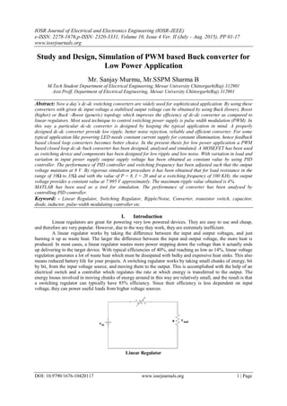
  • 1. IOSR Journal of Electrical and Electronics Engineering (IOSR-JEEE) e-ISSN: 2278-1676,p-ISSN: 2320-3331, Volume 10, Issue 4 Ver. II (July – Aug. 2015), PP 01-17 www.iosrjournals.org DOI: 10.9790/1676-10420117 www.iosrjournals.org 1 | Page Study and Design, Simulation of PWM based Buck converter for Low Power Application Mr. Sanjay Murmu, Mr.SSPM Sharma B M.Tech Student, Department of Electrical Engineering, Mewar University Chittorgarh(Raj) 312901 Asst.Proff, Department of Electrical Engineering, Mewar University Chittorgarh(Raj) 312901 Abstract: Now a day’s dc-dc switching converters are widely used for sophisticated application. By using these converters with given dc input voltage a stabilised output voltage can be obtained by using Buck (lower), Boost (higher) or Buck –Boost (generic) topology which improves the efficiency of dc-dc converter as compared to linear regulators. Most used technique to control switching power supply is pulse width modulation (PWM). In this way a particular dc-dc converter is designed by keeping the typical application in mind. A properly designed dc-dc converter provide low ripple, better noise rejection, reliable and efficient converter. For some typical application like powering LED needs constant current supply for constant illumination, hence feedback based closed loop converters becomes better choice. In the present thesis for low power application a PWM based closed loop dc-dc buck converter has been designed, analysed and simulated. A MOSEFET has been used as switching device and components has been designed for low ripple and low noise. With variation in load and variation in input power supply output supply voltage has been obtained as constant value by using PID controller. The performance of PID controller and switching frequency has been adjusted such that the output voltage maintain at 8 V. By rigorous simulation procedure it has been obtained that for load resistance in the range of 10Ω to 35Ω and with the value of P = 8, I = 20 and at a switching frequency of 100 KHz, the output voltage provides a constant value at 7.995 V approximately. The maximum ripple value obtained is 4%. MATLAB has been used as a tool for simulation. The performance of converter has been analysed by controlling PID controller. Keyword: - Linear Regulator, Switching Regulator, Ripple/Noise, Converter, transistor switch, capacitor, diode, inductor, pulse-width modulating controller etc. I. Introduction Linear regulators are great for powering very low powered devices. They are easy to use and cheap, and therefore are very popular. However, due to the way they work, they are extremely inefficient. A linear regulator works by taking the difference between the input and output voltages, and just burning it up as waste heat. The larger the difference between the input and output voltage, the more heat is produced. In most cases, a linear regulator wastes more power stepping down the voltage than it actually ends up delivering to the target device. With typical efficiencies of 40%, and reaching as low as 14%, linear voltage regulation generates a lot of waste heat which must be dissipated with bulky and expensive heat sinks. This also means reduced battery life for your projects. A switching regulator works by taking small chunks of energy, bit by bit, from the input voltage source, and moving them to the output. This is accomplished with the help of an electrical switch and a controller which regulates the rate at which energy is transferred to the output. The energy losses involved in moving chunks of energy around in this way are relatively small, and the result is that a switching regulator can typically have 85% efficiency. Since their efficiency is less dependent on input voltage, they can power useful loads from higher voltage sources. Linear Regulator
  • 2. Study and Design, Simulation of PWM basedBuck converter for Low Power Application DOI: 10.9790/1676-10420117 www.iosrjournals.org 2 | Page A simple Linear Regulator. If we consider an example, where Vin= 12V and we want to have a Vout= 8V. In this case we need to drop 4 volts across the regulator. Using standard power equation: P = V*I If the output current = 10A, this will result in 10 A * 4 V = 40 W. Now the regulator must dissipate 40 W of heat energy. This results in a mere 66.6% efficiency for the linear regulator and a lot of wasted power which is normally transformed into heat. Provision for heat sinks for cooling makes the regulator bulky and large. Hence, where size and efficiency are critical, linear voltage regulators cannot be used. Figure 2 is a very basic switching regulator. The switching regulator is a simple switch (and hence ideally no resistance or very low resistance). This switch goes on and off at a fixed rate (usually between 50 KHz to 100 KHz) as show Switching Regulator The Duty Cycle for the switch is determined by the Eq. Duty Cycle = Vout Vin The time that the switch remains closed during each switch cycle is varied to maintain a constant output voltage. The switching regulator is much more efficient than the linear regulator achieving efficiencies as high as 80% to 95% in some circuits. In contrast, the linear regulator usually exhibits only 50% to 60% efficiency. With higher efficiency smaller heat sinks will be required because lesser heat is dissipated. Comparison between Linear Regulator and Switching Regulator Linear Switching Function Only step down; input voltage must be greater than output. Step up, Step down, or inverts Complexity Low, which usually requires only the regulator and low value bypass capacitors. Medium to high, which usually requires inductor, diode, an filter caps in addition to the IC; for high power circuits, external FFTs are needed Ripple/Noise Low; no ripple, better noise rejection. Medium to high, due to ripple at switching rate. Efficiency Low to medium, But actual battery life depends on load current and battery voltage over time; high if Vin-Vout difference is small. High, except at very low load currents(µA), where switch mode quiescent current is usually higher Size Small to medium in portable designs, but may be larger if heat sinking is needed Larger than linear at low power, but smaller at power levels for which linear requires a heat sink. Total cost Low Medium to high, largely due to external components. Waste heat High, if average load and/or input/output voltage difference are high. Low as components usually run cool for power levels below 12W DC-DC Converter DC-DC converters are electronic devices that are used whenever we want to change DC electrical power efficiently from one voltage level to another. In the previous chapter we mentioned the drawbacks of doing this with a linear regulator. Types of Converters Currently, dc/dc converters can be divided into two broad categories: • Non-isolated dc/dc converters • Isolated dc/dc converters
  • 3. Study and Design, Simulation of PWM basedBuck converter for Low Power Application DOI: 10.9790/1676-10420117 www.iosrjournals.org 3 | Page Non-Isolated DC/DC Converters The non-isolated converter usually employs an inductor, and there is no dc voltage isolation between the input and the output. The vast majority of applications do not require dc isolation between input and output voltages. The non-isolated dc-dc converter has a dc path between its input and output. Battery-based systems that don’t use the ac power line represent a major application for non-isolated dc-dc converters. Point-of-load dc-dc converters that draw input power from an isolated dc-dc converter, such as a bus converter, represent another widely used non-isolated application. Most of these dc-dc converter ICs use either an internal or external synchronous rectifier. Their only magnetic component is usually an output inductor and thus less susceptible to generating electromagnetic interference. For the same power and voltage levels, it usually has lower cost and fewer components while requiring less pc-board area than an isolated dc-dc converter. For lower voltages (12V) non-isolated buck converters can be used. Isolated DC/DC Converters For safety considerations, there must be isolation between an electronic system’s ac input and dc output. Isolation requirements cover all systems operating from the ac power line, which can include an isolated front-end ac-dc power supply followed by an isolated “brick” dc-dc converter, followed by a non-isolated point- of-load converter. Typical isolation voltages for ac-dc and dc-dc power supplies run from 1500 to 4000V, depending on the application. An isolated converter employs a transformer to provide dc isolation between the input and output voltage which eliminates the dc path between the two. Isolated dc-dc converters use a switching transformer whose secondary is either diode-or synchronous- rectified to produce a dc output voltage using an inductor capacitor output filter. This configuration has the advantage of producing multiple output voltages by adding secondary transformer windings. For higher input voltages (48V) transformer isolated converters are more viable Buck Converter – Theory of Operation The name “Buck Converter” presumably evolves from the fact that the input voltage is bucked/chopped or attenuated, in amplitude and a lower amplitude voltage appears at the output. A buck converter, or step-down voltage regulator, provides non-isolated, switch-mode dc-dc conversion with the advantages of simplicity and low cost. Figure 3 shows a simplified non-isolated buck converter that accepts a dc input and uses pulse-width modulation (PWM) of switching frequency to control the output of an internal power MOSFET. An external diode, together with external inductor and output capacitor, produces the regulated dc output. . Non isolated Buck Regulator The buck converter here onwards is introduced using the evolutionary approach. Let us consider the circuit in Figure 4(a), containing a single pole double-throw switch.
  • 4. Study and Design, Simulation of PWM basedBuck converter for Low Power Application DOI: 10.9790/1676-10420117 www.iosrjournals.org 4 | Page Buck Converter The output voltage equals the input voltage when the switch is in position 1 and it is zero when the switch is in position 2. By varying the duration for which the switch is in position 1 and 2, it can be seen that the average output voltage can be varied, but the output voltage is not pure dc. The circuit in (a) can be modified as shown in belwo by adding an inductor in series with the load resistor. An inductor reduces ripple in current passing through it and the output voltage would contain less ripple content since the current through the load resistor is the same as that of the inductor. When the switch is in position A, the current through the inductor increases and the energy stored in the inductor increases. When the switch is in position 2, the inductor acts as a source and maintains the current through the load resistor. During this period, the energy stored in the inductor decreases and its current falls. It is important to note that there is continuous conduction through the load for this circuit. If the time constant due to the inductor and load resistor is relatively large compared with the period for which the switch is in position 1 or 2, then the rise and fall of current through inductor is more or less linear, as shown in Figure 5. Effect of an Inductor A capacitor reduces the ripple content in voltage across it, whereas an inductor smoothes the current passing through it. The combined action of LC filter reduces the ripple in output to a very low level. Circuit with an LC Filter With the circuit in Figurer it is possible to have a power semiconductor switch to correspond to the switch in position 1 and a diode in position 2. The circuit that results is shown in Figure 7. When the switch is in position 2, the current will pass through the diode. The important thing now is the controlling of the power semiconductor switch.
  • 5. Study and Design, Simulation of PWM basedBuck converter for Low Power Application DOI: 10.9790/1676-10420117 www.iosrjournals.org 5 | Page Buck converter without feedback The circuit in Figure Bulk converter without feedback can be regarded as the most elementary buck converter without a feedback. The Buck Converter transfers small packets of energy with the help of a power switch, a diode, and an inductor and is accompanied by an output filter capacitor and input filter. All the other topologies such as the Boost, Buck-Boost Converter etc, vary by the different arrangement of these basic components. This circuit can be further modified by adding the feedback part which is integral for a stabilizes the output. Such a circuit is shown in the Figurers below. Step down Buck Converter with feedback The PWM Controller above figure compares a portion of the rectified dc output with a voltage reference (Vref) and varies the PWM duty cycle to maintain a constant dc output voltage. If the output voltage wants to increase, the PWM lowers its duty cycle to reduce the regulated output, keeping it at its proper voltage level. Conversely, if the output voltage tends to go down, the feedback causes the PWM duty cycle to increase and maintain the proper output. A buck converter or step-down switch mode power supply can also be called a switch mode regulator Different components in the Buck Converter Buck converter consists of five standard components:  transistor switch (active switch)  capacitor  diode (passive switch)  inductor  pulse-width modulating controller Switch In its crudest form a switch can be a toggle switch which switches between supply voltage and ground. But for all practical applications which we shall consider we will deal with transistors. Transistors chosen for use in switching power supplies must have fast switching times and should be able to withstand the voltage spikes produced by the inductor. The input on the gate of the transistor is normally a Pulse Width Modulated (PWM) signal which will determine the ON and OFF time. Sizing of the power switch is determined by the load current and off-state voltage capability. Operating Frequency The operating frequency determines the performance of the switch. Switching frequency selection is typically determined by efficiency requirements. There is now a growing trend in research work and new power supply designs in increasing the switching frequencies. The higher is the switching frequency, the smaller the physical size and component value. The reason for this is to reduce even further the overall size of the power supply in line with miniaturisation trends in electronic and computer systems. Capacitor Capacitor provides the filtering action by providing a path for the harmonic currents away from the load. Output capacitance (across the load) is required to minimize the voltage overshoot and ripple present at the output of a step-down converter. The capacitor is large enough so that its voltage does not have any noticeable change during the time the switch is off. Large overshoots are caused by insufficient output capacitance, and
  • 6. Study and Design, Simulation of PWM basedBuck converter for Low Power Application DOI: 10.9790/1676-10420117 www.iosrjournals.org 6 | Page large voltage ripple is caused by insufficient capacitance as well as a high equivalent-series resistance (ESR) in the output capacitor. The maximum allowed output voltage overshoot and ripple are usually specified at the time of design. Thus, to meet the ripple specification for a step-down converter circuit, we must include an output capacitor with ample capacitance and low ESR. Inductor The function of the inductor is to limit the current slew rate (limit the current in rush) through the power switch when the circuit is ON. The current through the inductor cannot change suddenly. When the current through an inductor tends to fall, the inductor tends to maintain the current by acting as a source. This limits the otherwise high-peak current that would be limited by the switch resistance alone. The key advantage is when the inductor is used to drop voltage, it stores energy. Also the inductor controls the percent of the ripple and determines whether or not the circuit is operating in the continuous mode. Pulse-width modulating controller Pulse Width Modulation (PWM) Design and analysis of Buck Converter The buck converter is used for step down operation. A buck converter with its output filter area Open loop buck converter When the switch S1 is on and S2 is off, the input voltage appears across the inductor and current in inductor increases linearly. In the same cycle the capacitor is charged. When the switch S1 is on and S2 is off, the voltage across the inductor is reversed. However, current in the inductor cannot change instantaneously and the current starts decreasing linearly. In this cycle also the capacitor is also charged with the energy stored in the inductor. Continuous Mode / Discontinuous Mode During the ON state and then the subsequent OFF state the Buck Converter can operate in Continuous Mode or Discontinuous Mode. The difference between the two is that in CCM the current in the inductor does not fall to zero. (a) Continuous mode (b) Discontinuous mode
  • 7. Study and Design, Simulation of PWM basedBuck converter for Low Power Application DOI: 10.9790/1676-10420117 www.iosrjournals.org 7 | Page Calculation for Duty Ratio For calculation of the duty ratio we will first of all assume that the converter is in steady state. The switches are treated as being ideal, and the losses in the inductive and the capacitive elements are neglected. Also it is important to point out that the following analysis does not include any parasitic resistances (all ideal case). The analysis also has the assumption that the converter is operating in Continuous conduction mode only i.e. iL(t) > 0.When the switch is on for time duration ton , the switch conducts the inductor current and the diode becomes reverse biased. This results in a positive voltage vL=Vd-Vo across the inductor in Figure 12 (a). This voltage causes a linear increase in the inductor current iL. When the switch is turned off, because of the inductive energy storage, iL continues to flow. This current now flows through the diode, and vL = −Vo in Figure. Since in steady-state operation waveform must repeat from one time period to the next, the integral of the inductor voltage L v over one time period must be zero, where Ts = ton+ toff . 𝑣𝐿 𝑇𝑠 0 𝑑𝑡 = 𝑣𝐿 𝑡𝑜𝑛 0 𝑑𝑡 + 𝑣𝐿 𝑇𝑠 𝑡𝑜𝑛 𝑑𝑡 = 0 It implies that areas A and B must be equal. Therefore, 𝑉𝑑 − 𝑉𝑜 𝑡 𝑜𝑛 = 𝑉𝑜 𝑇𝑠 − 𝑡 𝑜𝑛 or 𝑉𝑜 𝑉𝑑 = 𝑡 𝑜𝑛 𝑇𝑠 = 𝐷 𝐷𝑢𝑡𝑦 𝑅𝑎𝑡𝑖𝑜 Hence in this mode, the voltage output varies linearly with the duty ratio of the switch for a given input voltage and does not depend on any other circuit parameter. Step down converter circuit states for CCM mode: (a) Switch on; (b) Switch off Calculation for Inductor We can derive a simplified differential equation based on the assumption that the voltage across the load, and thereby across the capacitor, is fairly constant. The differential equation in terms of the current through the inductor, when the switch is closed, may now be written as 𝐿𝑖 𝐿 𝑡 𝑑𝑡 = 𝑉𝑑 − 𝑉𝑜 − − − − − − − − − − − − − (1) Assuming that the circuit has assumed steady state hence there may already be some current in the inductor, ILmin , just prior to the closing of switch S. Hence for a time interval 0 ≤t ≤ Ton = DT , gives: 𝑖 𝐿 𝑡 = 𝑉𝑑 − 𝑉𝑜 𝐿 𝑡 + 𝐼𝐿,𝑚𝑖𝑛 − − − − − − − − − − − −(2) The inductor current increases linearly with time and attains its maximum value Il,max as t→TON =DT such that
  • 8. Study and Design, Simulation of PWM basedBuck converter for Low Power Application DOI: 10.9790/1676-10420117 www.iosrjournals.org 8 | Page 𝐼𝐿,𝑚𝑎𝑥 = 𝑉𝑑 − 𝑉𝑜 𝐿 𝐷𝑇 + 𝐼𝐿,𝑚𝑖𝑛 − − − − − − − − − − − (3) Defining the change in the current from its minimum to maximum value as the peak-to-peak current ripple ΔIL , the equation 4-6 yields an expression for ΔIL ,as 𝛥𝐼𝐿 = 𝐼𝐿,𝑚𝑎𝑥 − 𝐼𝐿,𝑚𝑖𝑛 = 𝑉𝑑 − 𝑉𝑜 𝐿 𝐷𝑇 − − − − − − − − − − − −(4) Note that the current ripple is directly proportional to D, the duty cycle, upon which we may not have any control because of the output voltage requirement. However, it is inversely proportional to the inductance L upon which we can exert some control. Thus, the current ripple can be controlled by a proper selection of the inductor. Let us now analyze the circuit when the switch is in its open position. The inductor current completes its path through the lower side MOSFET and the corresponding differential equation, for OFF 0 ≤ t ≤ TOFF, is 𝐿 𝑑𝑖 𝐿 t 𝑑𝑡 = −𝑉𝑜 − − − − − − − − − − − − − (5) From the solution of the above first-order differential equation, we obtain 𝑖 𝐿 𝑡 = − 𝑉𝑜 𝐿 𝑡 + 𝐼𝐿,𝑚𝑎𝑥 − − − − − − − − − (6) Where IL,max is the maximum value of the current in the inductor at the opening of the switch or the beginning of the off period. As t →Toff = (1−D )T, the inductor current decreases to its minimum value IL,min such that 𝐼𝐿,𝑚𝑖𝑛 = − 𝑉𝑜 𝐿 1 − 𝐷 𝑇 + 𝐼𝐿,𝑚𝑎𝑥 − − − − − − − −(7) The Eq. 7 yields another expression for the peak-to-peak current ripple as ∆𝐼𝐿 = 𝐼𝐿,𝑚𝑎𝑥 − 𝐼𝐿,𝑚𝑖𝑛 = 𝑉𝑜 𝐿 1 − 𝐷 𝑇 − − − − − − − −(8) Inductor Current The current through the inductor as given by Eq. 2 during the on time and by Eq. 6 during the off time is sketched in the Figure 13. The average current in the inductor must be equal to the dc current through the load. That is, 𝐼𝐿,𝑎𝑣𝑔 = 𝐼𝑜 = 𝑉𝑜 𝑅 − − − − − − − −(9) The expressions for the maximum and minimum currents through the inductor may now be written as 𝐼𝐿,𝑚𝑎𝑥 = 𝐼𝐿,𝑎𝑣𝑔 + ∆𝐼𝐿 2 = 𝑉𝑜 𝑅 + 𝑉𝑜 2𝐿 1 − 𝐷 𝑇 − − − − − − − (10) 𝐼𝐿,𝑚𝑖𝑛 = 𝐼𝐿,𝑎𝑣𝑔 − ∆𝐼𝐿 2 = 𝑉𝑜 𝑅 − 𝑉𝑜 2𝐿 1 − 𝐷 𝑇 − − − − − (11) The current supplied by the source varies from IL,min to IL,max during the time the switch is closed and is zero otherwise as shown in Figure 14.
  • 9. Study and Design, Simulation of PWM basedBuck converter for Low Power Application DOI: 10.9790/1676-10420117 www.iosrjournals.org 9 | Page Source Current When the switch, the inductor, and the capacitor are treated as ideal elements, the average power dissipated by them is zero. Consequently, the average power supplied by the source must be equal to the average power delivered to the load. That is, 𝑉𝑑 𝐼 𝑑 = 𝑉𝑜 𝐼𝑜 = 𝐷𝑉𝑠 𝐼𝑠 − − − − − −(12) This equation helps us express the average source current in terms of the average load current as 𝐼𝑠 = 𝐷𝐼𝑜 the current through the lower side MOSFET is shown in Figure 15. Its average value is 𝐼𝐿𝑠 = 1 − 𝐷 𝐼𝑜 − − − − − − − − 13 Current through low side of Mosefet We know the fact that the buck converter can either operate in its continuous conduction mode or discontinuous mode. When it operates in the continuous conduction mode, there is always a current in the inductor. The minimum current in the continuous conduction mode can be zero. Consequently, there is a minimum value of the inductor that ensures its continuous conduction mode. It can be obtained from Eq. 11 by setting IL min to zero as 𝑉𝑜 𝑅 − 𝑉𝑜 2𝐿 𝑚𝑖𝑛 1 − 𝐷 𝑇 = 0 − − − − − − − (14) Hence, 𝐿 𝑚𝑖𝑛 = 1 − 𝐷 2 𝑅𝑇 = 1 − 𝐷 2𝑓 𝑅 − − − −(15) Calculation for Capacitor The output capacitor is assumed to be so large as to yield vo(t)=Vo . However, the ripple in the output voltage with a practical value of capacitance can be calculated by considering the waveforms shown in Figure 16 for a continuous conduction mode of operation. Assuming that all of the ripple component in iL flows through the capacitor and its average component flow through the load resistor, the shaded area in Figure 16 represents an additional charge ΔQ. Output Voltage ripple in a step down Converter
  • 10. Study and Design, Simulation of PWM basedBuck converter for Low Power Application DOI: 10.9790/1676-10420117 www.iosrjournals.org 10 | Page Therefore, the peak-to-peak voltage ripple ∆𝑉𝑜 can be written as ∆𝑉𝑜 = ∆𝑄 𝐶 = 1 𝐶 1 2 𝛻𝐼𝐿 2 𝑇𝑠 2 − − − − − − − − − (16) From Figure 16 during toff ∆𝐼𝐿 = 𝑉𝑜 𝐿 1 − 𝐷 𝑇𝑠 − − − − − − − −(17) Therefore, substituting ΔIL from Eq. 17 into the Eq. 16 gives ∆𝑉𝑜 = 𝑇𝑠 8𝐶 𝑉𝑜 𝐿 1 − 𝐷 𝑇𝑠 − − − − − − − (18) ∆𝑉𝑜 𝑉𝑜 = 1 8 𝑇𝑠 2 1 − 𝐷 𝐿𝐶 = 𝜋2 2 1 − 𝐷 𝑓𝑐 𝑓𝑠 2 − − − − − − − (19) Where switching frequency fs =1/T and 𝑓𝑐 = 1 2𝜋 𝐿𝐶 − − − − − (20) Equation 19 shows that the voltage ripple can be minimized by selecting a corner frequency fc of the low pass filter at the output such that fc <<fs. Also, the ripple is independent of the output load power, so long as the converter operates in the continuous-conduction mode. We should note that in switch-mode dc power supplies, the percentage ripple in the output voltage are usually specified to be less than, for instance, 1%. The analysis carried out above assumes ideal components and if we were to make the analysis using all the non-ideal components it would make the derivation a bit more complex with a lot of other parameters included in the final equation. But for the calculation of initial values of the components the above approximations does result in reasonable values. It is also important to realize here that the ESR and ESL are also important and can even dominate. More about how the non-ideality can affect the overall system can be found on [6]. PWM Controller The heart of a switching power supply is its switch control circuit (controller). One of the key objectives in designing a controller for the power converter is to obtain tight output voltage regulation under different line and load conditions [7]. Often, the control circuit is a negative-feedback control loop connected to the switch through a comparator and a Pulse Width Modulator (PWM). The switch control signal (PWM), controls the state (on or off) of the switch. This control circuit regulates the output voltage against changes in the load and the Input voltage. PWM PWM is the method of choice to control modern power electronics circuits. The basic idea is to control the duty cycle of a switch such that a load sees a controllable average voltage. To achieve this, the switching frequency (repetition frequency for the PWM signal) is chosen high enough that the load cannot follow the individual switching events and they appear just a “blur” to the load, which reacts only to the average state of the switch. With pulse-width modulation control, the regulation of output voltage is achieved by varying the duty cycle of the switch, keeping the frequency of operation constant. Duty cycle refers to the ratio of the period for which the power semiconductor is kept ON to the cycle period.
  • 11. Study and Design, Simulation of PWM basedBuck converter for Low Power Application DOI: 10.9790/1676-10420117 www.iosrjournals.org 11 | Page Comparator and Voltage to PWM Converter Switching power supplies rely on negative feedback to maintain the output voltages at their specified value. To accomplish this, a differential amplifier is used to sense the difference between an ideal voltage (the reference voltage) and the actual output voltage to establish a small error signal (v control). Voltage Reference Controller The PWM switching at a constant switching frequency is generated by comparing a signal-level control voltage v control with a repetitive waveform as shown in Figure 18. PWM Comparator Signals The frequency of the repetitive waveform with a constant peak, which is shown to be a saw tooth, establishes the switching frequency. This frequency is kept constant in a PWM control and is chosen to be in a few hundred kilohertz range. When the amplified error signal, which varies very slowly with time relative to the switching frequency, is greater than the saw tooth waveform, the switch control signal becomes HIGH, causing the switch to turn on. Otherwise, the switch is off. So when the circuit output voltage changes, v control also changes causing the comparator threshold to change. Consequently, the output pulse width also changes. This duty cycle change then moves the output voltage to reduce to error signal to zero, thus completing the control loop. In terms of, v control and the peak of the saw tooth waveform Vst in the switch duty ratio can be expressed as D = ton Ts = Vcontrol Vst − − − − − − − 21 PID Controller A proportional–integral–derivative controller (PID controller) is a generic control loop feedback mechanism (controller) widely used in industrial control systems – a PID is the most commonly used feedback controller. A PID controller calculates an "error" value as the difference between a measured process variable and a desired set point. The controller attempts to minimize the error by adjusting the process control inputs. With the use of PI controller the output voltage of the buck converter set to a desired value. In this chapter we vary the value of P and I so that our desired output will be achieved. For this first we set the value of P=0, and then vary the value of I=0, 10, 20, 30, 40 and so on. Then change the value of P=3, and then vary the value of I=0, 10, 20, 30, 40 and so on. Similar process will be repeated such that our desired value will not achieve.
  • 12. Study and Design, Simulation of PWM basedBuck converter for Low Power Application DOI: 10.9790/1676-10420117 www.iosrjournals.org 12 | Page Closed loop Buck Converter Shim Power Simulation Diagram Waveform of VL, IL, VC, IC, VO, IO when P=0 and I=10
  • 13. Study and Design, Simulation of PWM basedBuck converter for Low Power Application DOI: 10.9790/1676-10420117 www.iosrjournals.org 13 | Page Waveform of VL, IL, VC, IC, VO, IO when P=0 and I=20 Waveform of VL, IL, VC, IC, VO, IO when P=0 and I=30
  • 14. Study and Design, Simulation of PWM basedBuck converter for Low Power Application DOI: 10.9790/1676-10420117 www.iosrjournals.org 14 | Page Waveform of VL, IL, VC, IC, VO, IO when P=3 and I=0 Different Values of VL, IL, VC, IC, VO, IO when P=0 and I=10 to 40 I VO IO VL IL VC IC 10 7.298 0.7298 0.8606 0.2055 7.298 0.5243 20 7.699 0.7699 1.05 0.213 7.699 0.5569 30 7.833 0.7833 0.7386 0.2154 7.833 0.5679 40 7.896 0.7896 1.205 0.2183 7.896 0.5714 Simulation of dc-dc buck converter for open loop :- Simulate the open loop dc-dc buck converter and getting the output response.first we vary the load resistance keeping the supply voltage constant and then vary the supply voltage by keeping the load resistance constant.the output response is show. Open loop Buck Converter SimPower Simulation Diagram
  • 15. Study and Design, Simulation of PWM basedBuck converter for Low Power Application DOI: 10.9790/1676-10420117 www.iosrjournals.org 15 | Page Waveform of VL, IL, VC, IC, VO, IO when Load=10Ω Waveform of VL, IL, VC, IC, VO, IO when Load =15Ω Waveform of VL, IL, VC, IC, VO, IO when Supply Voltage VS=12V
  • 16. Study and Design, Simulation of PWM basedBuck converter for Low Power Application DOI: 10.9790/1676-10420117 www.iosrjournals.org 16 | Page Open loop Buck Converter Simulated Values vs. Load Resistance R R VO IO VL IL VC IC 10 5.232 0.5233 1.879 0.09876 5.232 0.4244 15 8.662 0.5775 1.26 0.09143 8.662 0.4861 20 9.108 0.4554 4.013 0.1036 9.108 0.3518 25 9.433 0.3773 3.969 0.09374 9.433 0.2836 30 9.677 0.3226 4.046 0.08731 9.677 0.2352 35 9.863 0.2818 3.859 0.08169 9.863 0.2001 40 10.03 0.2508 3.756 0.07387 10.03 0.1769 45 10.15 0.2256 3.828 0.06937 10.15 0.1562 50 10.24 0.2047 3.871 0.06758 10.24 0.1371 Open loop Buck Converter Simulated Values vs. Supply Voltage VS VS VO IO VL IL VC IC 8 5.232 0.5232 1.879 0.09876 5.232 0.4244 8.5 5.566 0.5566 1.101 0.09785 5.566 0.4588 9 5.91 0.591 0.1577 0.08391 5.91 0.5071 9.5 6.239 0.6239 0.5234 0.0916 6.239 0.5323 10 6.568 0.6568 0.4543 0.09439 6.568 0.5625 Closed loop Buck Converter Sims Power Simulation Diagram Closed loop Buck Converter Simulated Values v/s. Load Resistance R R VO IO VL IL VC IC 10 7.955 0.7955 1.188 0.04656 7.955 0.7489 15 7.969 0.5312 1.262 0.03165 7.969 0.4996 20 7.978 0.3989 1.093 0.02438 7.978 0.3745 25 7.986 0.3194 1.236 0.02064 7.986 0.2988 30 7.992 0.2664 1.316 0.01675 7.992 0.2496 35 7.998 0.2285 1.299 0.01505 7.998 0.2135 40 8.003 0.2001 1.294 0.01318 8.003 0.1869 45 8.007 0.1779 1.257 0.01227 8.007 0.1657 50 8.012 0.1602 1.332 0.01127 8.012 0.140 Closed loop Buck Converter Simulated Values v/s Supply Voltage VS VO IO VL IL VC IC 8 7.743 0.7743 0.1186 1.364 7.743 0.5901 8.5 7.888 0.7888 0.4903 0.1228 7.888 0.666 9 7.893 0.7893 0.06857 0.08389 7.893 0.7055 9.5 7.911 0.7911 0.135 0.05655 7.911 0.7345 10 7.922 0.7922 0.2823 0.04702 7.922 0.7452 Figure 58 Graph for Output voltage and reference Voltage vs Load 7.92 7.93 7.94 7.95 7.96 7.97 7.98 7.99 8 8.01 8.02 10 15 20 25 30 35 40 45 50 Output Voltage ReferenceVoltge
  • 17. Study and Design, Simulation of PWM basedBuck converter for Low Power Application DOI: 10.9790/1676-10420117 www.iosrjournals.org 17 | Page Graph for Output voltage and reference Voltage vs Supply Voltag II. Result and Conclusion Of variation of load as well as variation in supply voltage. The simulation result shows that the output voltage vary only maximum up to 3% if we vary increase the load resistance by 250% and lower the supply voltage by 66.6%. The converter can be utilised for low power application such as to drive light Future scope 1. In the present thesis we use asynchronous buck converter, by using the synchronous buck converter efficiency can be improved. 2. Here we design for low power applications, by changing the parameter of buck converter, high power application can be done. 3. By the variation of supply voltage, load and constant parameter (P & I) output voltage can be set for a particular application where it is desired. References [1]. http://www.rason.org/Projects/swregdes/swregdes.htm [2]. http://services.eng.uts.edu.au/~venkat/pe_html/ch07s1/ch07s1p1.htm [3]. http://www.maxim-ic.com/appnotes.cfm/appnote_number/751 [4]. Michael D. Mulligan, Bill Broach, and Thomas H. Lee, “A Constant Frequency Method for Improving Light-Load Efficiency in Synchronous Buck Converters”, Power Electronics Letters, IEEE Volume 3, Issue 1, March 2005 Page(s): 24 – 29 [5]. R.D. Middlebrook and S. Cuk, "A General Unified Approach To Modelling Switching Converter Power Stages", IEEE Power Electronics Specialists Conference, 1976 Record, pp 18-34. [6]. http://en.wikipedia.org/wiki/Buck_converter [7]. http://www.irf.com/technical-info/appnotes/mosfet.pdf [8]. "History and Development of Switched-Mode Power Supplies Pre 1987" Available at: http://www.steve- w.dircon.co.uk/fleadh/mphil/history.htm [9]. http://www.planetanalog.com/features/power/showArticle.jhtml?articleID=193402327 [10]. SWITCHMODE Power Supplies, Reference Manual and Design Guide, ON Semiconductor. Available at: http://www.onsemi.com/pub/Collateral/SMPSRM-D.PDF [11]. Chin Chang, “Robust Control of DC-DC Converters: The Buck Converter”, Power Electronics Specialists Conference, 1995. 26th Annual IEEE Volume 2, Issue , 18-22 Jun 1995 Page(s):1094 - 1097 vol.2 [12]. M. H. Rashid, Power Electronics: Circuits, Devices and Applications (3rd Edition), Prentice Hall, 2003. [13]. N. Mohan , T. M. Undeland, W. P. Robbins, Power Electronics: Converters, Applications, and Design, 3rd Bk&Cdr edition, Wiley, 2002. [14]. R.D Middlebrook and S Cuk , “A general unified approach to modeling switching Converter Power stages,” in Proc. IEEE PESC Rec., pp. 18–34, 1976. [15]. A.J. Forsyth and S.V. Mollow, “Modeling and control of dc-dc converters,” IEE power engineering journal, vol. 12, no. 5, pp. 229– 236, Oct. 1998. [16]. V.S.C Raviraj and P.C. Sen, “Comparative Study of proportional-integral, Sliding-mode, and fuzzy logic controllers for power converters,” IEEE transaction on Industry applications, vol. 33, no. 2, pp. 518-524, Mar. /Apr. 1997. [17]. Ekaitz Zulueta Teodoro Rico1 Jose Maria Gonzalez de Durana,” HYBRID MODELING OF OPEN LOOP DC-DC CONVERTERS” REVISTA FACULTAD DE INGENIERIA, U.T.A. (CHILE), VOL. 11 N°2, 2003, pp. 41-47 [18]. Vorperian, V., “Simplified Analysis of PWM Converters Using the Model of the PWM Switch”, Aerospace and Electronic Systems, IEEE Transactions on, Volume:26, Issue: 2, March 1990 7.6 7.65 7.7 7.75 7.8 7.85 7.9 7.95 8 8.05 8 8.5 9 9.5 10 10.5 11 12 Voltage SupplyVoltage Output Voltage ReferenceVoltage