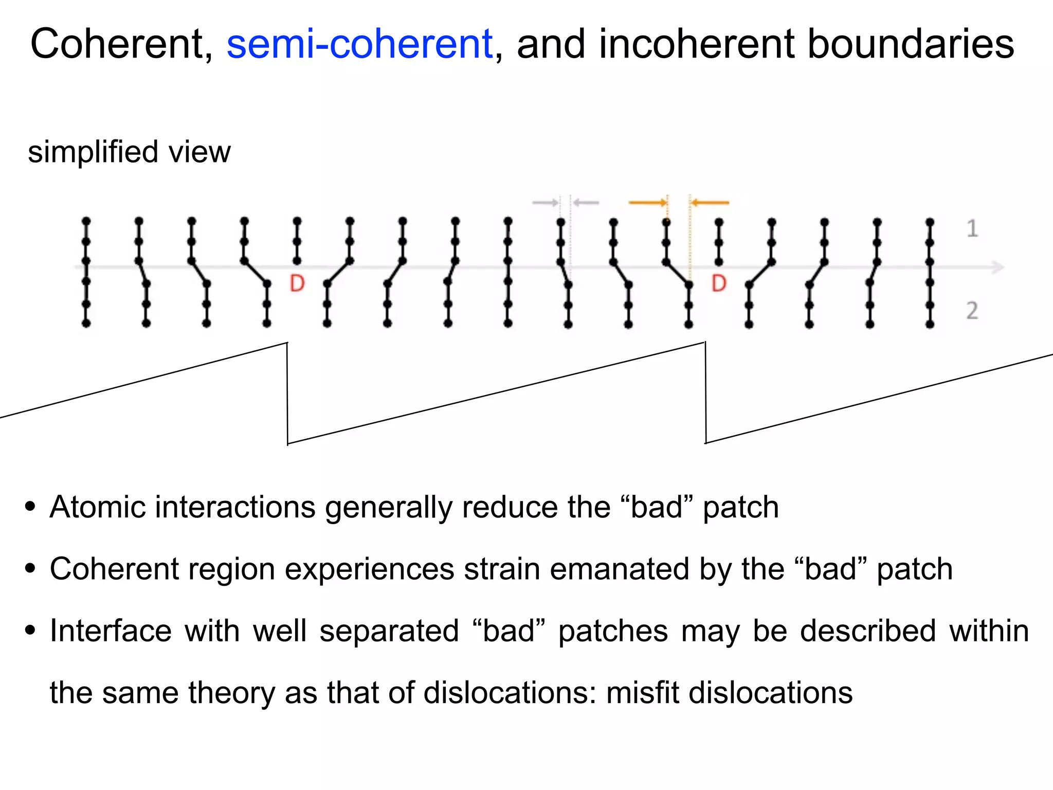
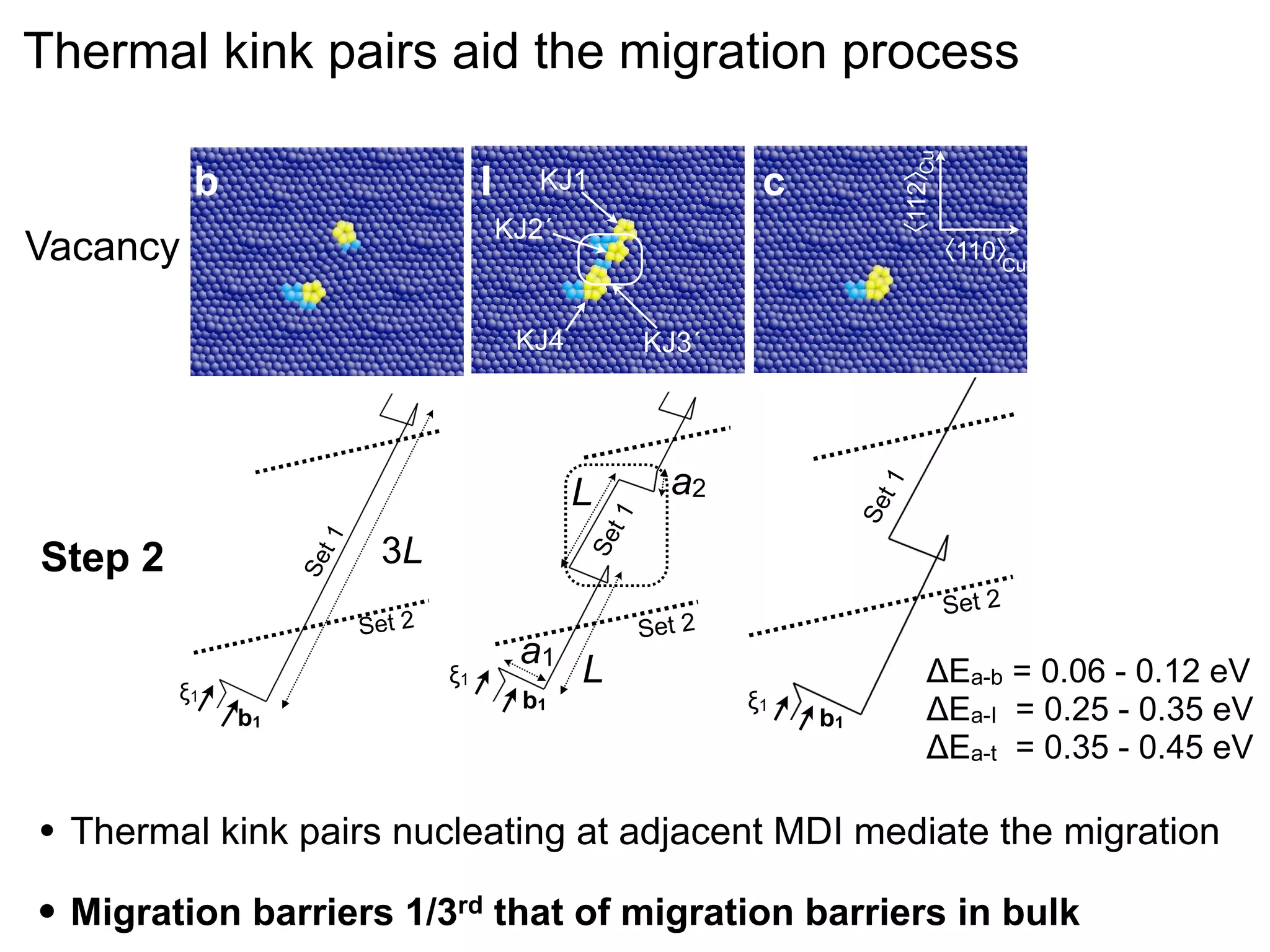
Download to read offline
![Internal interfaces enhance ionic conduction
•
•
•
Downloaded from www.sciencemag.org on September 17, 2011
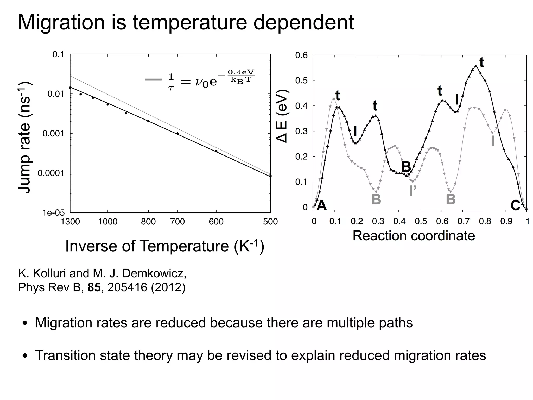
byand with the thickness of the lattice.shows that the large degraded interface structure when the YSZ layers
strains to match the STO YSZ, Because the frequency plots. In the presence of blocking effects
exceed the critical electrodes,
conductivity values in these heterostructures due
inbulk lattice constants of STO and YSZ are orig- to grain boundaries orthickness. a further
ee
ues Fig. 3. Dependence of the logarithm of the
in long-range ionic conductivity of the trilayers
his STO/YSZ/STO versus inverse temperature. The
to thickness range of the YSZ layer is 1 to 62 nm.
gi- Also included are the data of a single crystal
0.6
is (sc) of YSZ and a thin film (tf) 700 nm thick
1
[taken from (7)] with the same nominal
he composition. (Top inset) 400 K conductance
is of [YSZ1nm/STO10nm](ni/2) superlattices as a
gle function of the number of interfaces, ni.
eas (Bottom inset) Dependence of the conductgle ance of [STO10nm/YSZXnm/STO10nm] trilayers at
1.1
ior 500 K on YSZ layer thickness. Error bars are
ers according to a 1 nS uncertainty of the con1
ductance measurement.
ler
yer
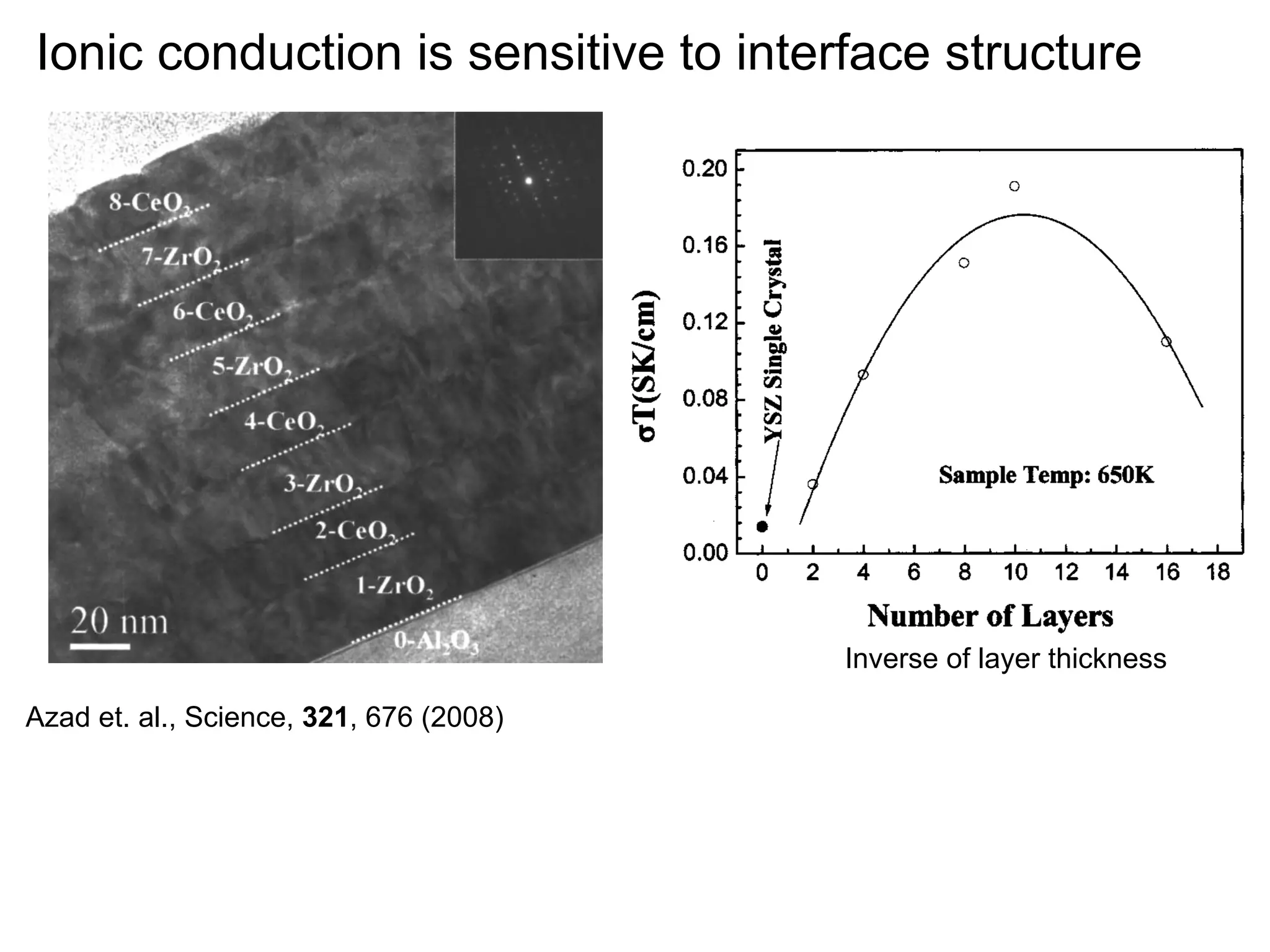
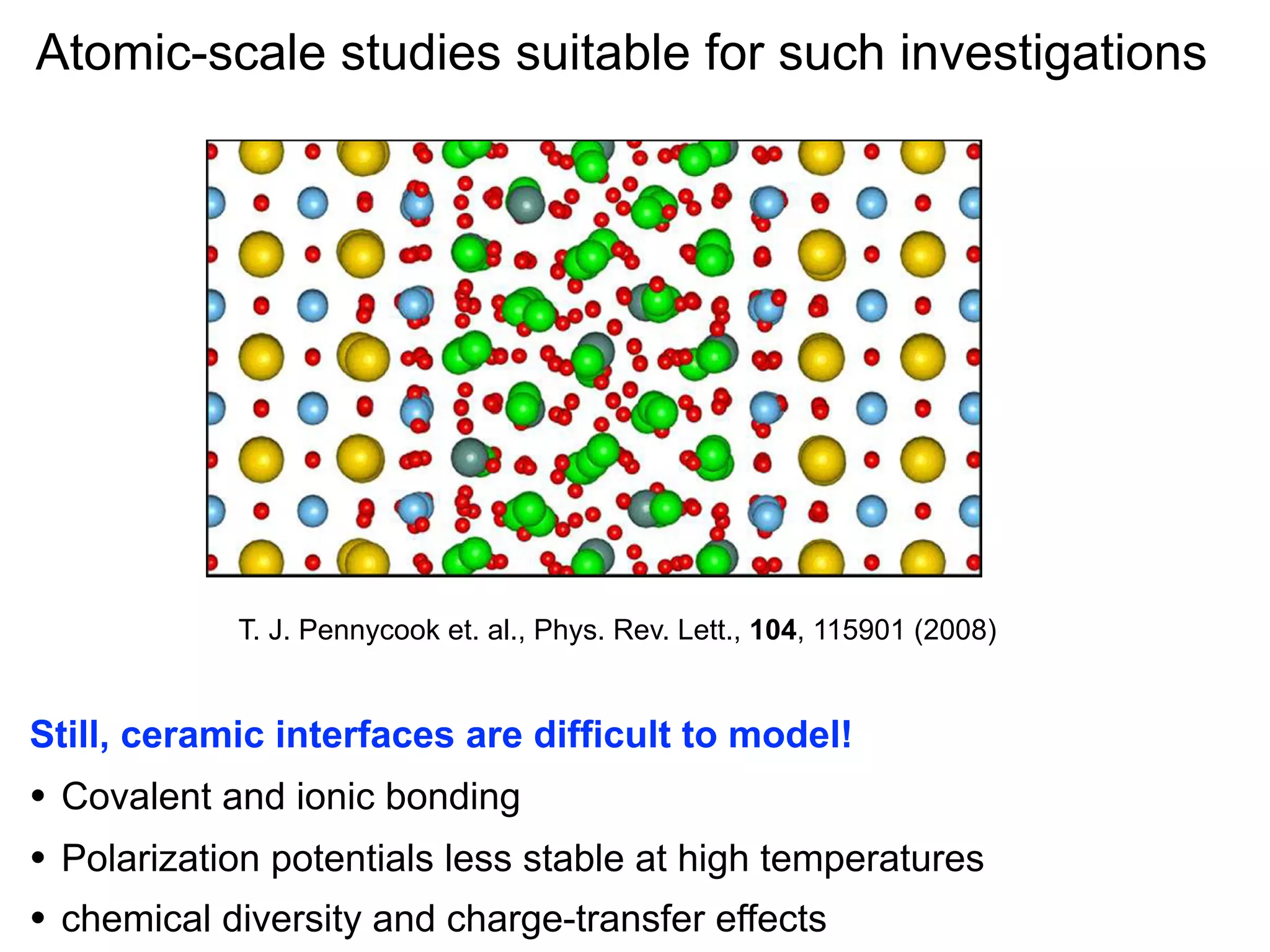
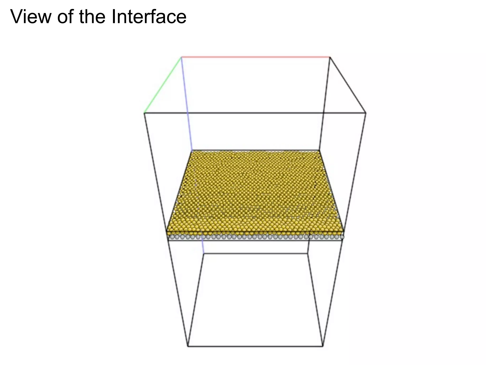
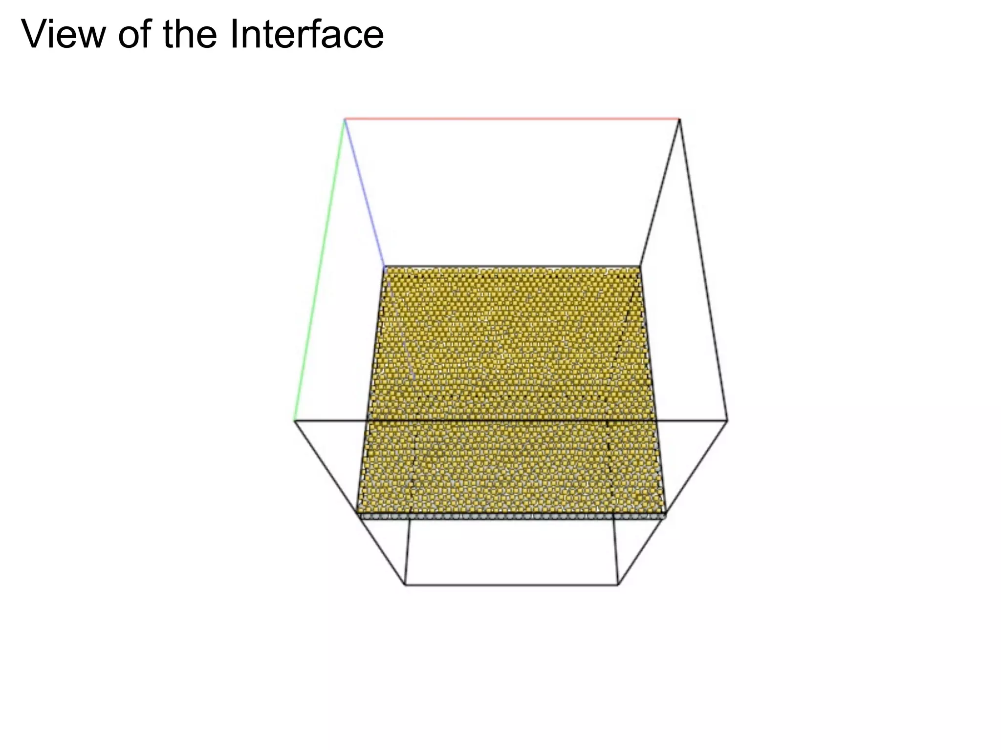
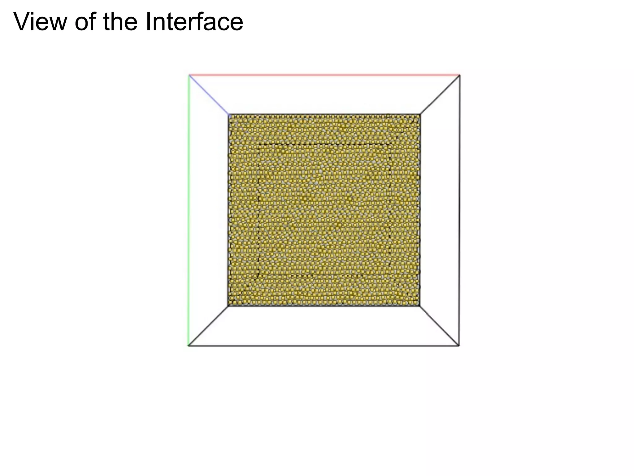
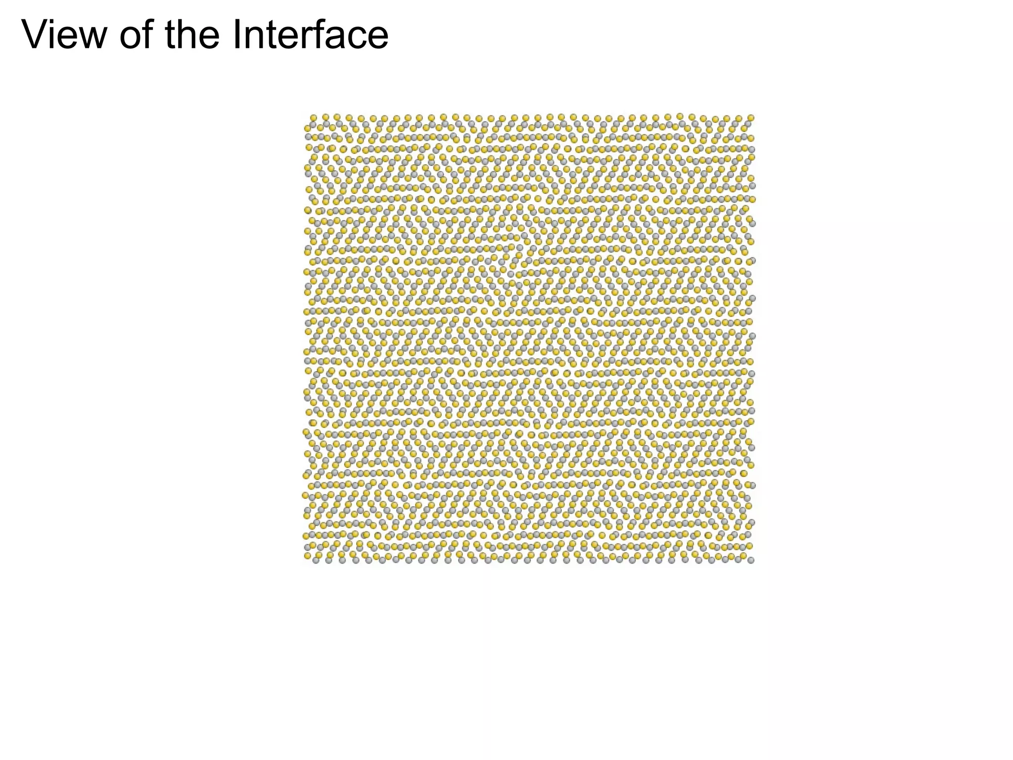
outFig. 1. (A) Z-contrast scanning transmission electron microscopy (STEM) image of the STO/YSZ interface of
J. Garcia-Barriocanal et. al., Science, 321, 676 (2008)
dcthe [YSZ1nm/STO10nm]9 superlattice (with nine repeats), obtained in the VG Microscopes HB603U
sesmicroscope. A yellow arrow marks the position of the YSZ layer. (Inset) Low-magnification image obtained
Why?
in the VG Microscopes HB501UX column. In both cases a white arrow indicates the growth direction. (B) EEL
he
sesspectra showing the O K edge obtained from the STO unit cell at the interface plane (red circles) and 4.5 nm
High defect concentrations
into the STO layer (black squares). (Inset) Ti L2,3 edges for the same positions, same color code. All spectra
vaare the result of averaging four individual spectra at these positions, with an acquisition time of 3 s each.
of Faster transport due to interface structure; Strain-enhanced diffusion
areFig. 2. Real part of the lateral
No conductivity versus freorselectrical space charge in this example but possible in other interfaces](https://image.slidesharecdn.com/aiche2012presentation-131231181926-phpapp02/75/AIChE-2012-Presentation-2-2048.jpg)


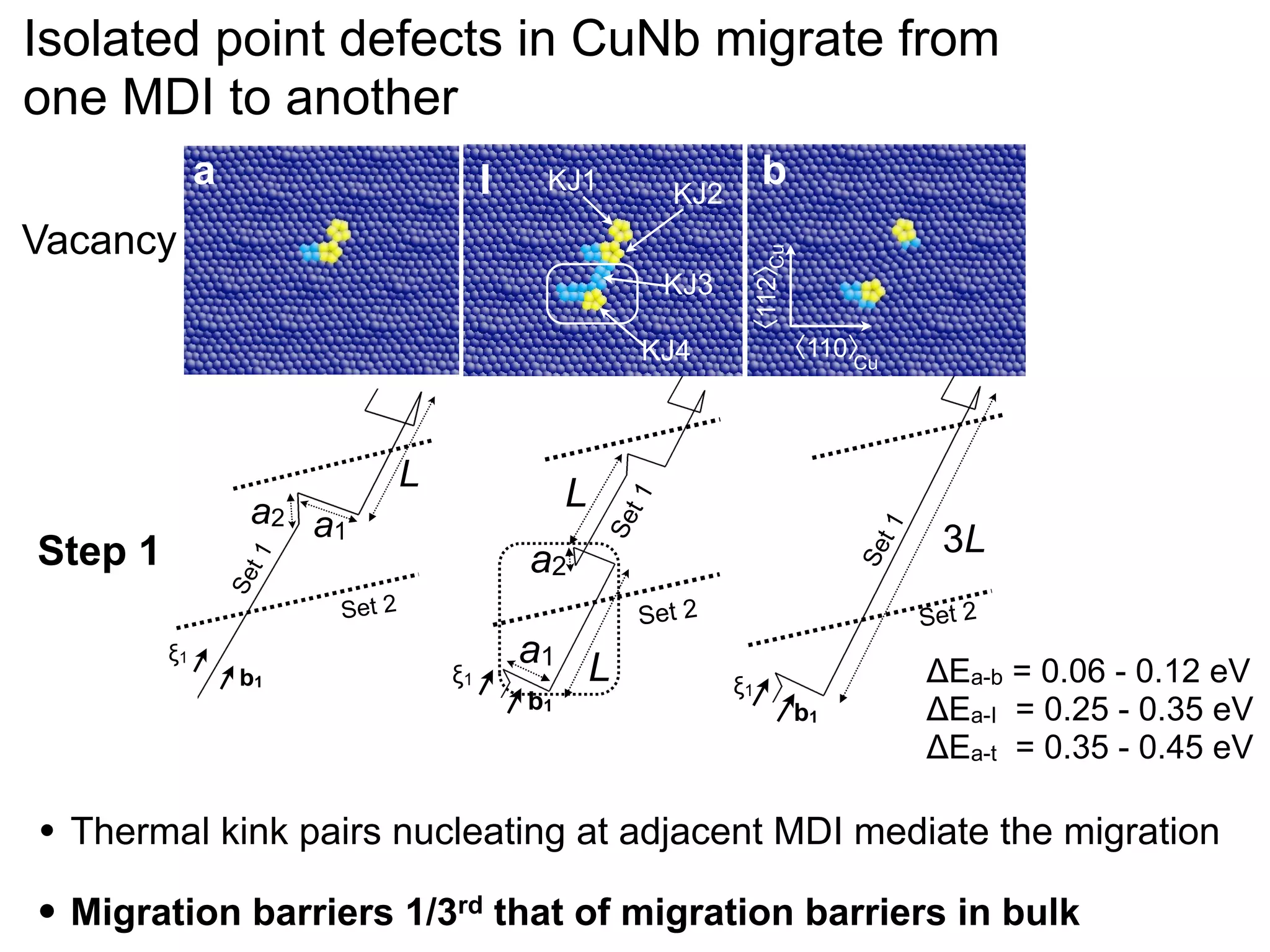
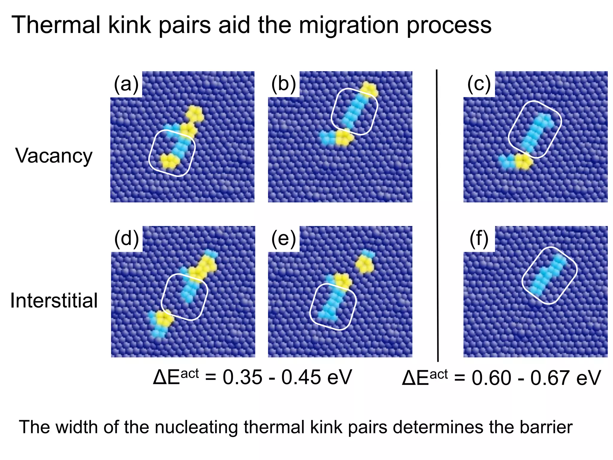
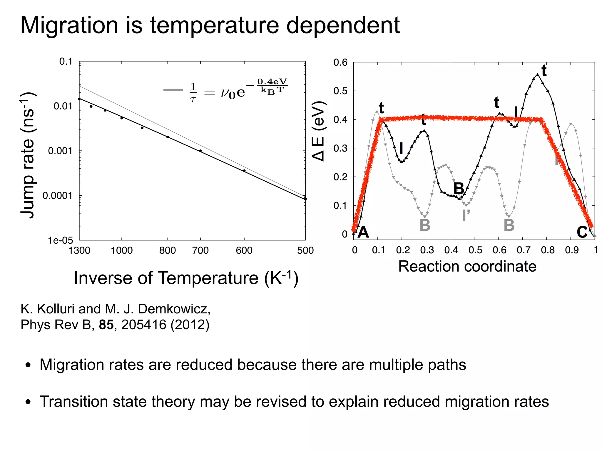
![jog, which is assumed constant for all states in our dislocation
model [and therefore does not appear in Eq. (1)], actually varies
along the direct migration path. To estimate the core energy
of the kink-jog, we summed differences in atomic energies
between the core atoms and corresponding atoms in a defectfree interface. The kink-jog core is taken to consist of 19 atoms:
the 5-atom ring in the Cu terminal plane and the 7 neighboring
Cu and Nb atoms from each of the two planes adjacent to the Cu
terminal plane. Core volumes were computed in an analogous
way. The core energies of the migrating jog are plotted as
filled triangles in Fig. 15(a) and are in good semiquantitative
agreement with the overall energy changes occurring along
the direct migration path. Core volumes are plotted as filled
circles.
Figure 15(b) shows the Cu and Nb interface planes with
a point defect in the extended state B. Arrows mark the
locations of the two kink-jogs and red lines mark the nominal
locations of set 2 misfit dislocation cores. The numbers are
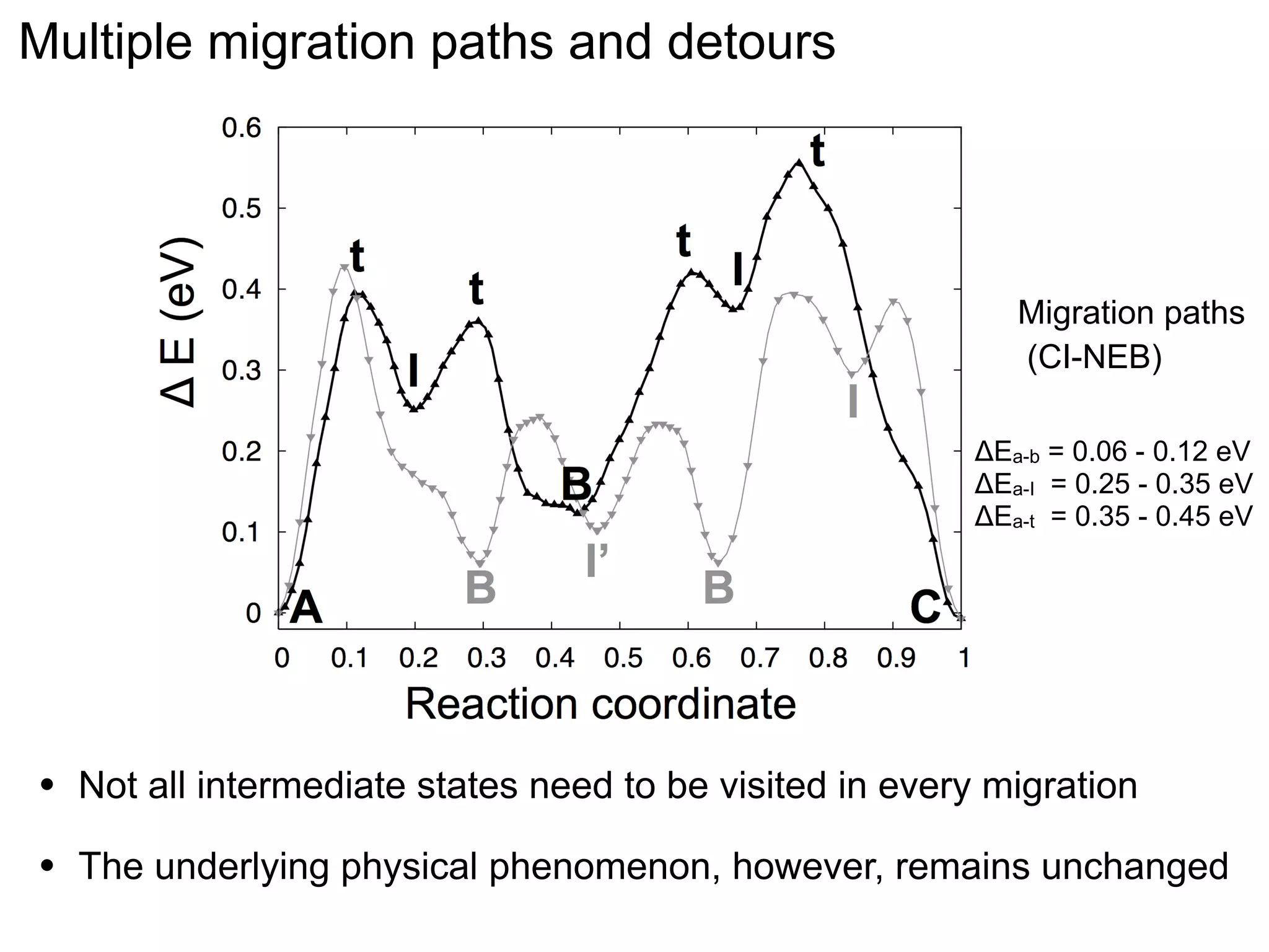
TABLE I. Transitions occurring during migration of individual
point defects that were considered in kMC simulations, their
corresponding activation energy barriers, and number of distinct end
states for a given start state.
Point defect migration rates from simulations
Transition
type
A→I
A→B
I (near A) → B
I (near A) → A
B→A
B→I
B→I
B→C
I (near C) → C
I (near C) → B
I →B
Activation energy
(eV)
Number of
distinct end states
0.40
0.40
0.15
0.15
0.35
0.35
0.20
0.35
0.15
0.15
0.15
2
2
1
1
1
2
1
1
1
1
1
205416-9
•
Hypothesis:
•
•
•
transition state theory is valid and
Rate-limiting step will determine the migration rate ≥ 0.4 eV
Validation:
•
kinetic Monte Carlo (since the migration path is not trivial)
•
Statistics from molecular dynamics](https://image.slidesharecdn.com/aiche2012presentation-131231181926-phpapp02/75/AIChE-2012-Presentation-36-2048.jpg)
![ln[(s!)p(t/τ,s)] = s ln(t/τ ) − t/τ.
(10)
Migration is temperature dependent
s are obtained for all three temperatures, confirming
0.1
tion that point defect1migration follows a Poisson
⇥
= 0 k 1T e
ig. 17). The jump rates for each temperature,
0.01
1
= 0e
y fitting, are plotted in Fig. 16(b) as filled gray
h uncertainties corresponding to the error in the
0.001
es fit. The gray line is the least-squares fit of Eq. (8)
obtained from MD. The activation energy obtained
0.0001
act
MC model (Eeff = 0.398 ± 0.002 eV) is well within
nty of 1e-05 activation energy found by fitting the MD
the
500
act
y, Eeff =1300 1000 0.045700 600
0.374 ± 800 eV.
Inverse of Temperature (K )
ctive attempt frequency for defect-1migration obfittingKolluri and M. J. Demkowicz, = 6.658 × 10⁹ ± 2.7 ×
K. the MD data is ν0
Phys Rev several orders of
is value is B, 85, 205416 (2012) magnitude lower than
mpt frequencies for point defect migration in fcc
• Migration −1 .72–74 A mechanistic interpretation paths
12
14 rates are reduced because there are multiple
, 10 −10 s
ow migration attempt frequency is not immediately
• Transition state theory may be revised to explain reduced migration rates
g. One possible explanation is that it arises from
number of atoms participating in the migration
Jump rate (ns-1)
Eact
e
kB T
B
0.4eV
kB T](https://image.slidesharecdn.com/aiche2012presentation-131231181926-phpapp02/75/AIChE-2012-Presentation-39-2048.jpg)


Mass transport at internal interfaces of inorganic materials - Ionic conduction is sensitive to interface structure, with interfaces enhancing ionic conduction due to high defect concentrations, strain-enhanced diffusion, and interface-modified structure (1-2 sentences) - Point defects at semicoherent metal interfaces like Cu-Nb delocalize across the interface and migrate between misfit dislocation arrays, with the lowest barrier for vacancy migration between 0.06-0.12 eV (1 sentence) - Understanding defect behavior at metal interfaces provides insights into modifying ion transport at ceramic interfaces like grain boundaries in materials like MgO (1 sentence)


