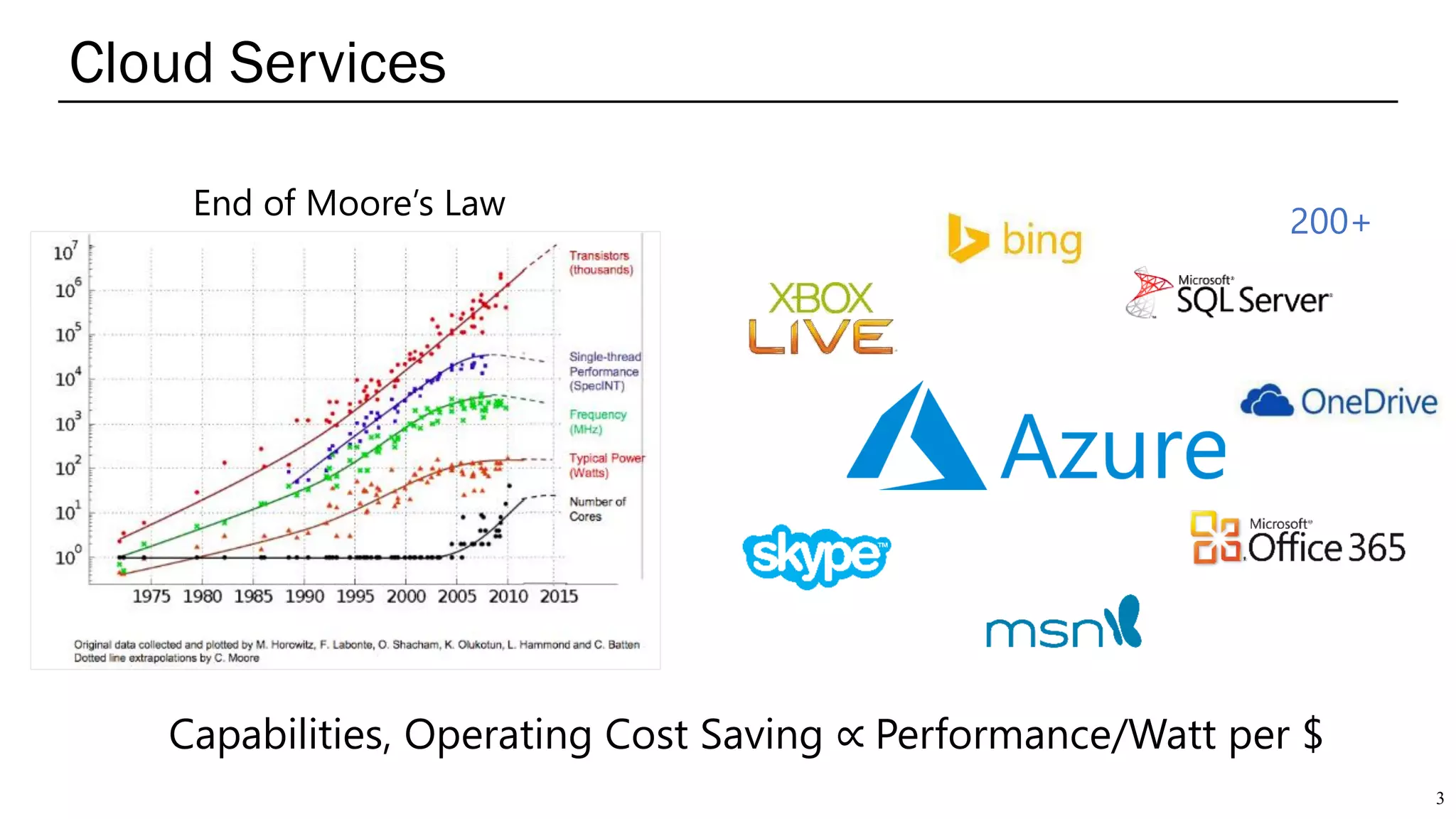
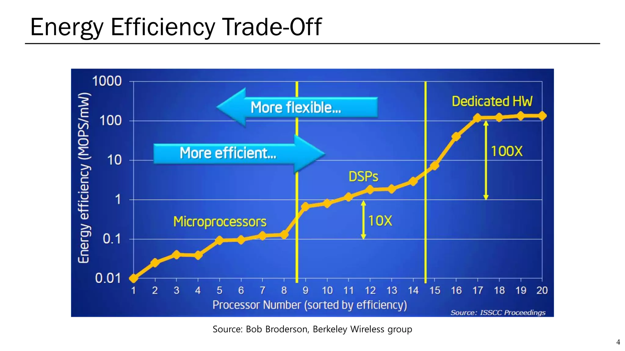
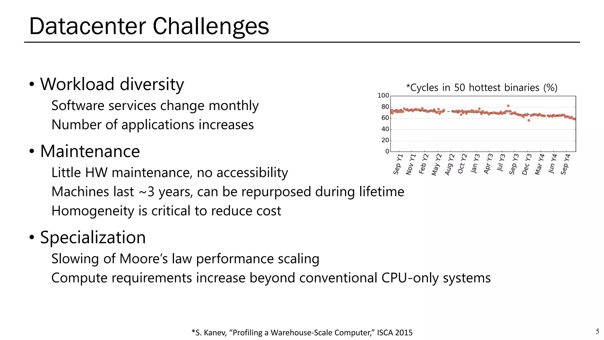
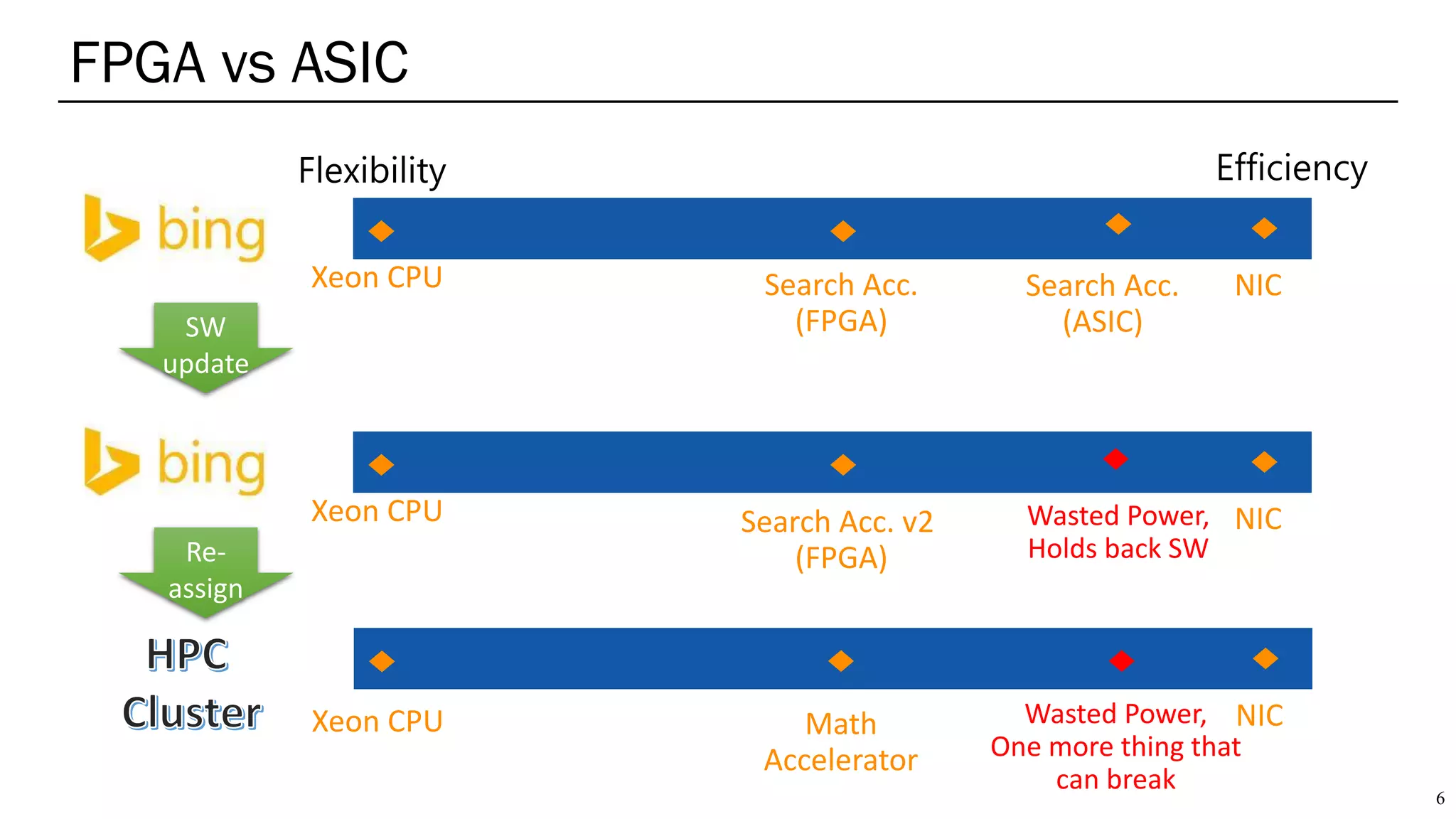
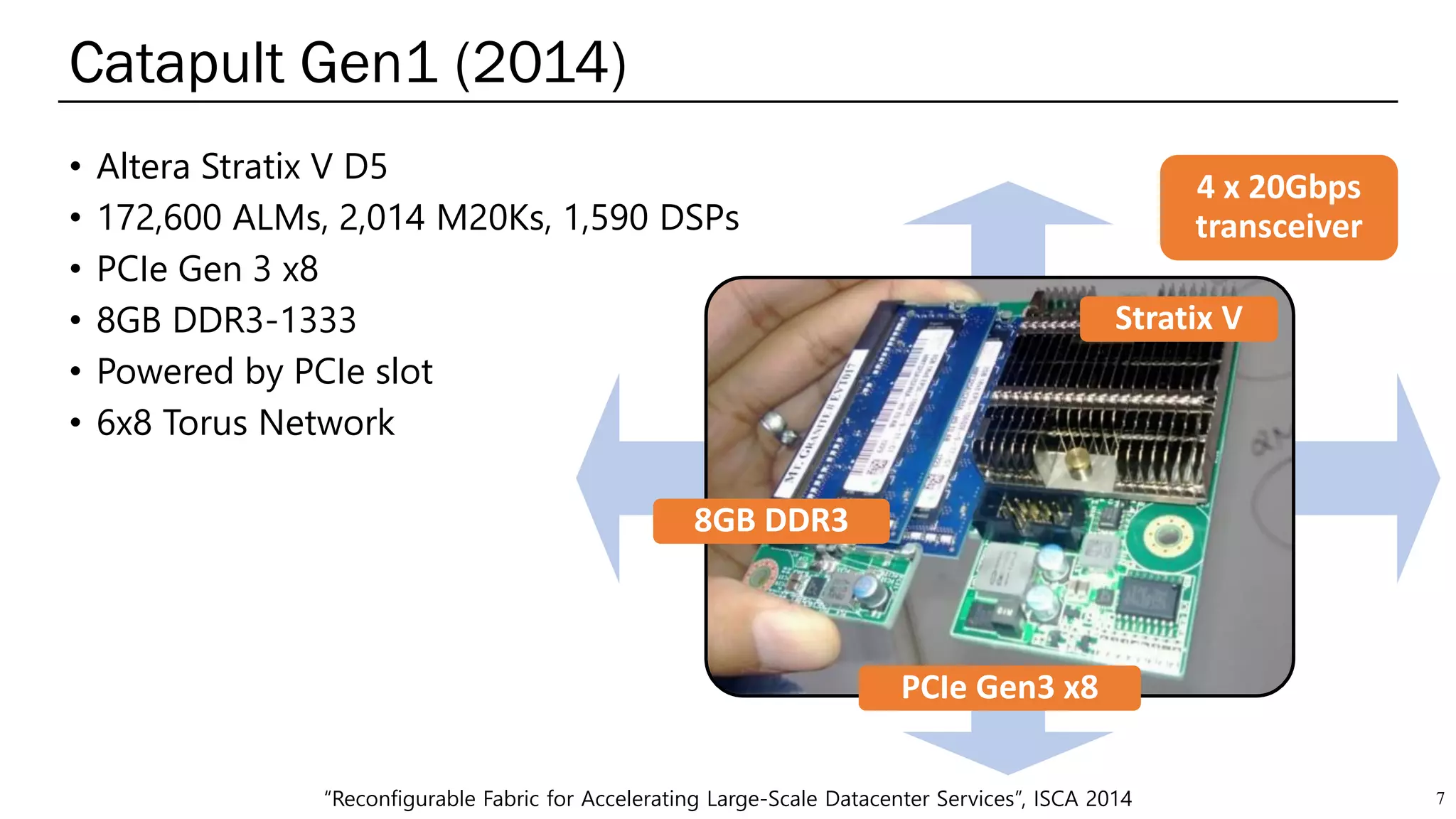
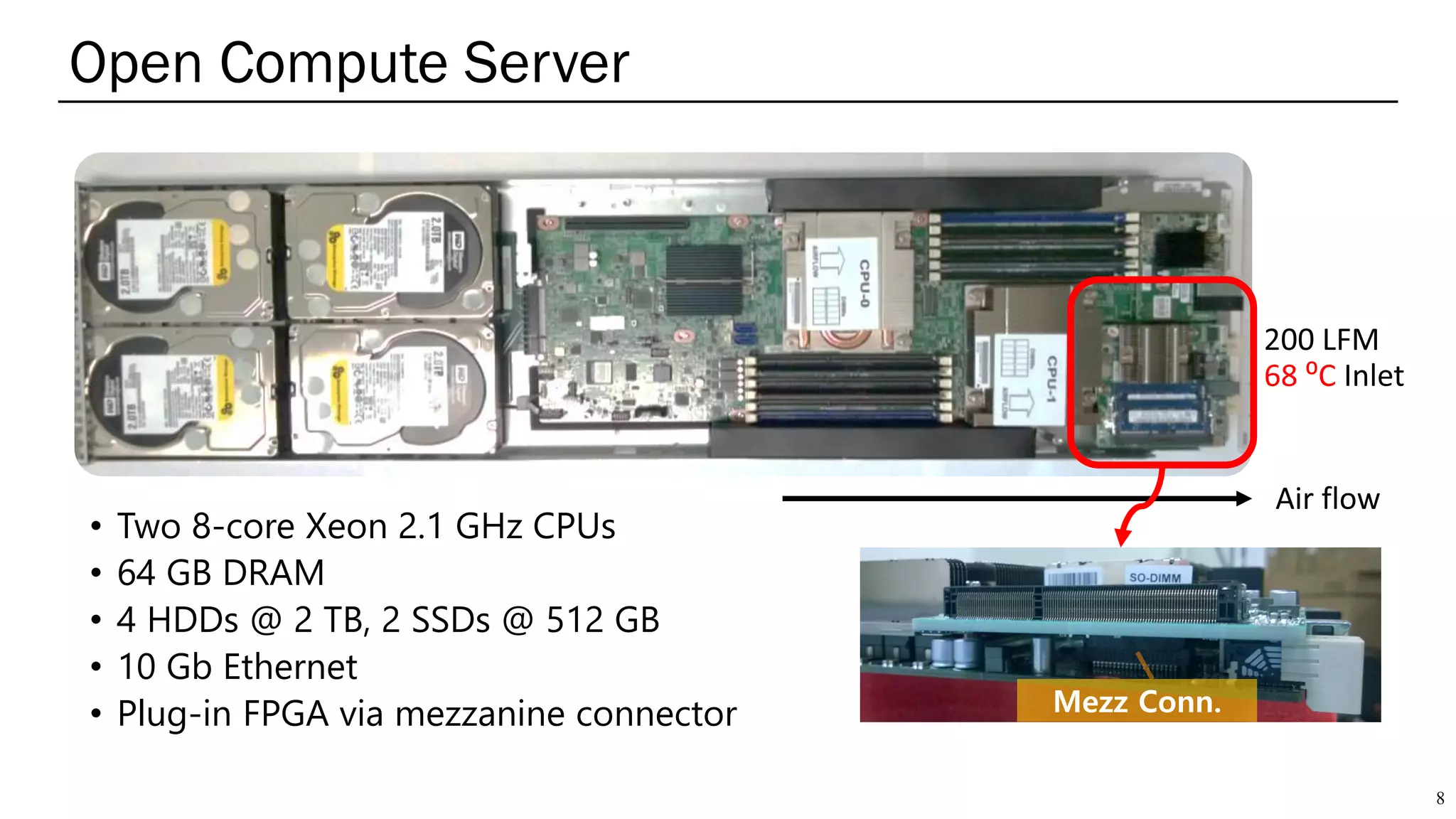
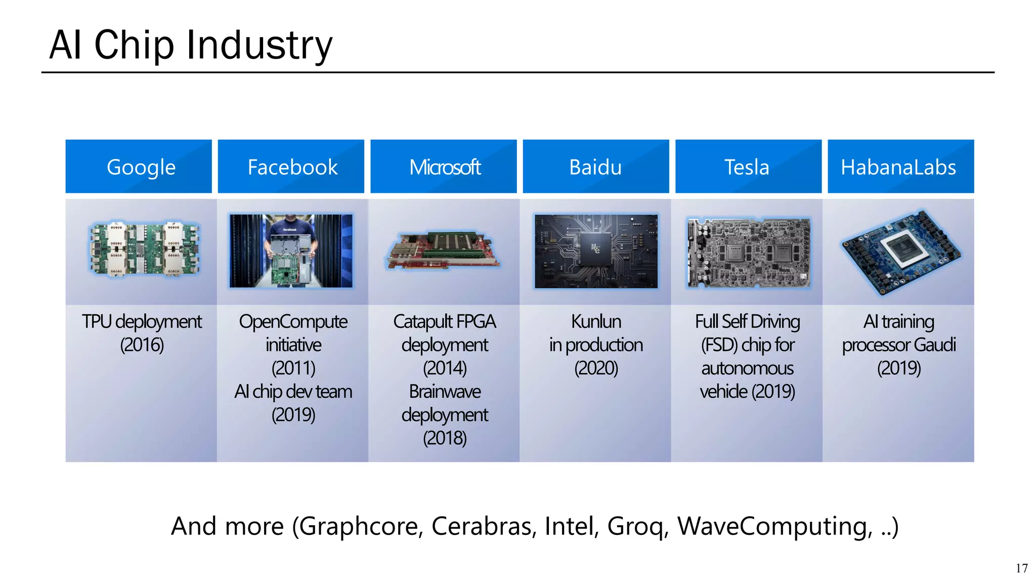
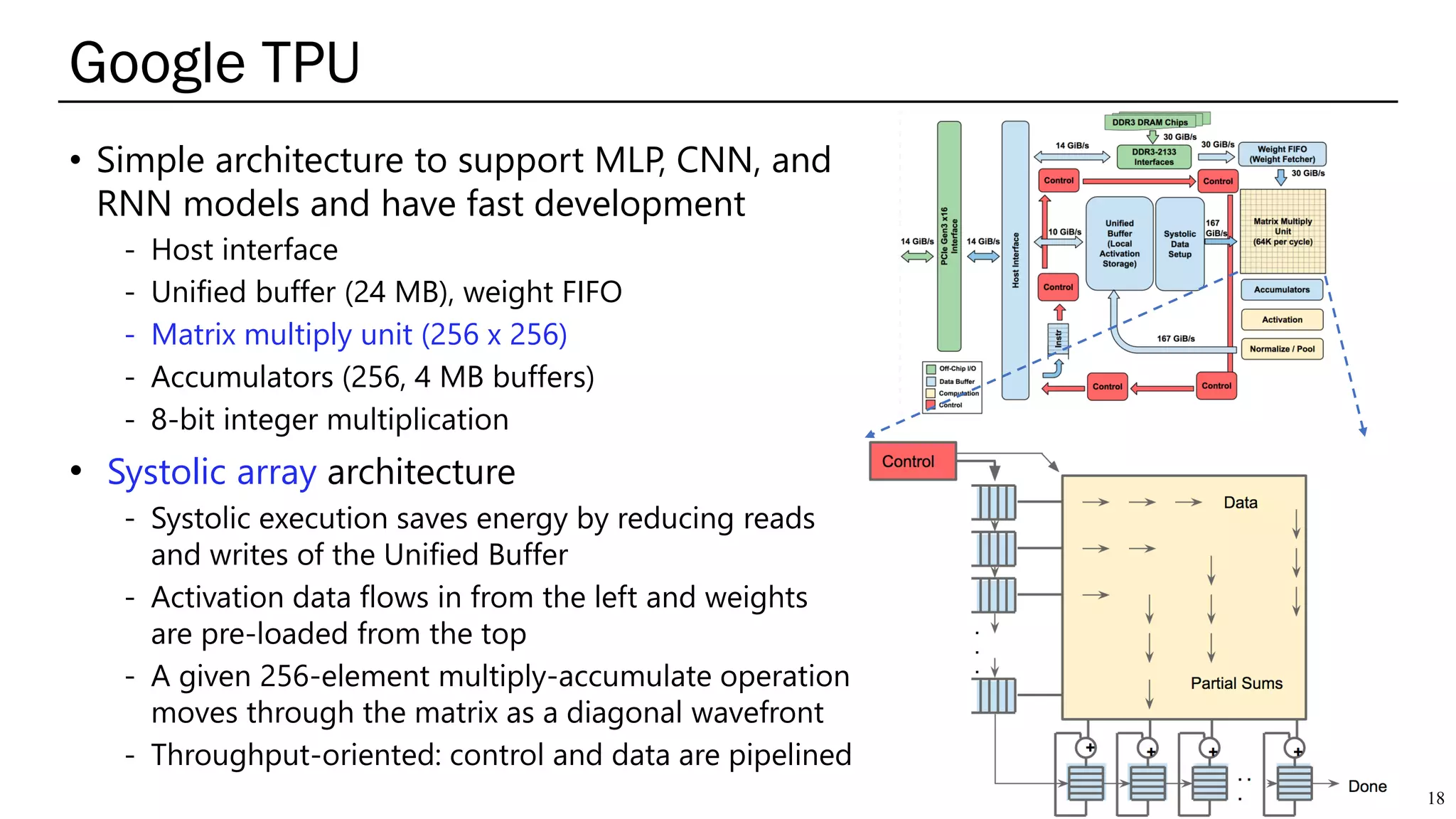
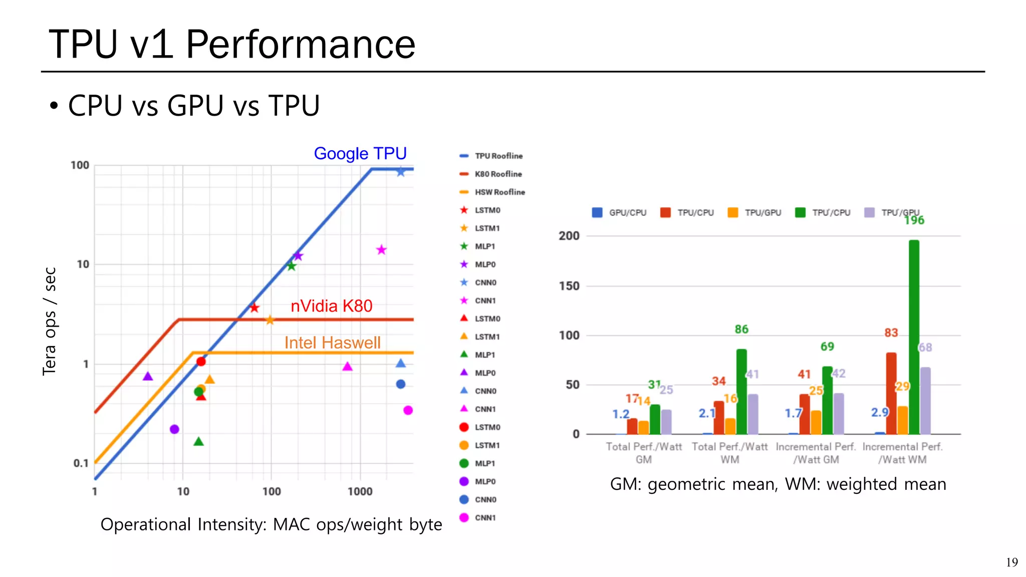
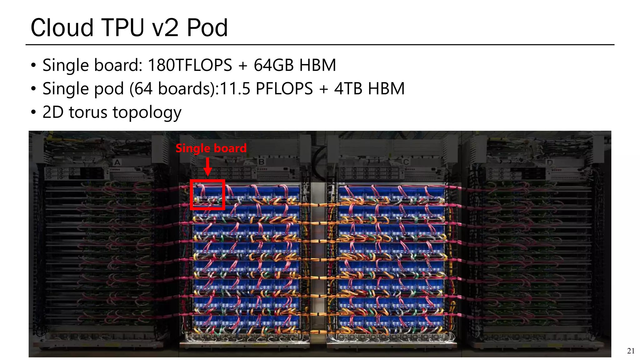
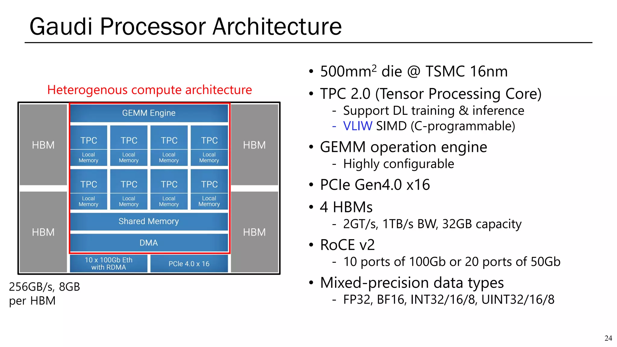
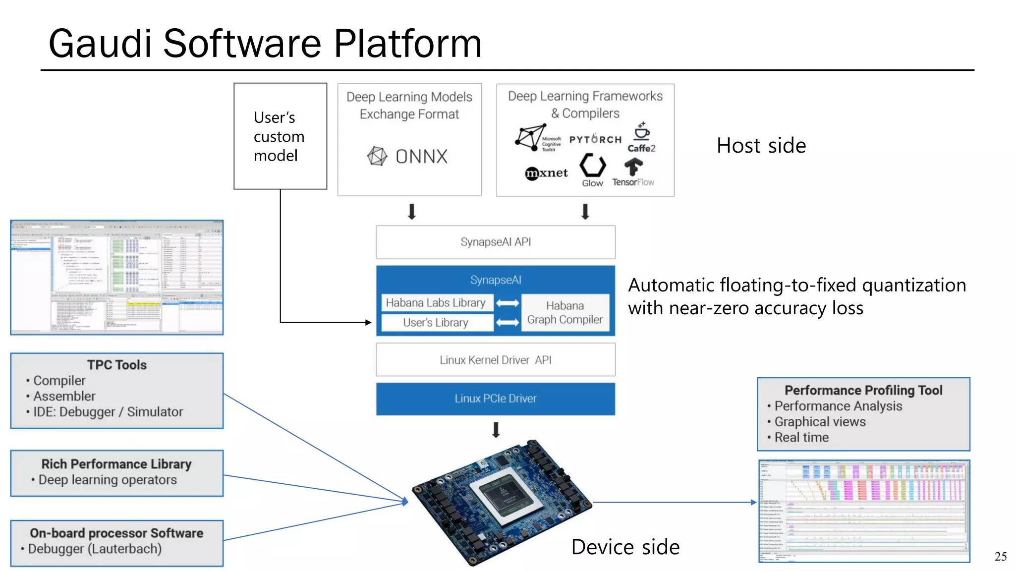
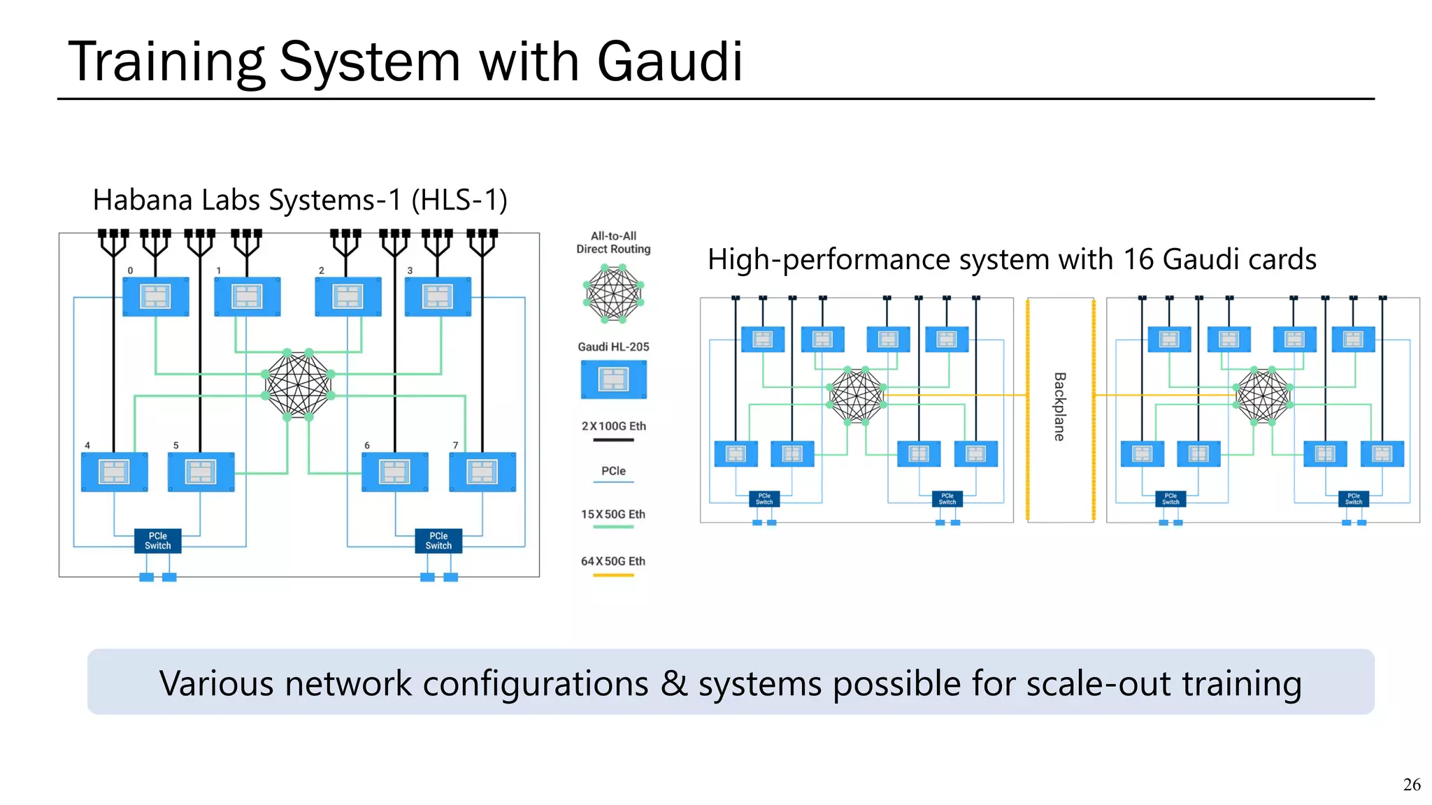
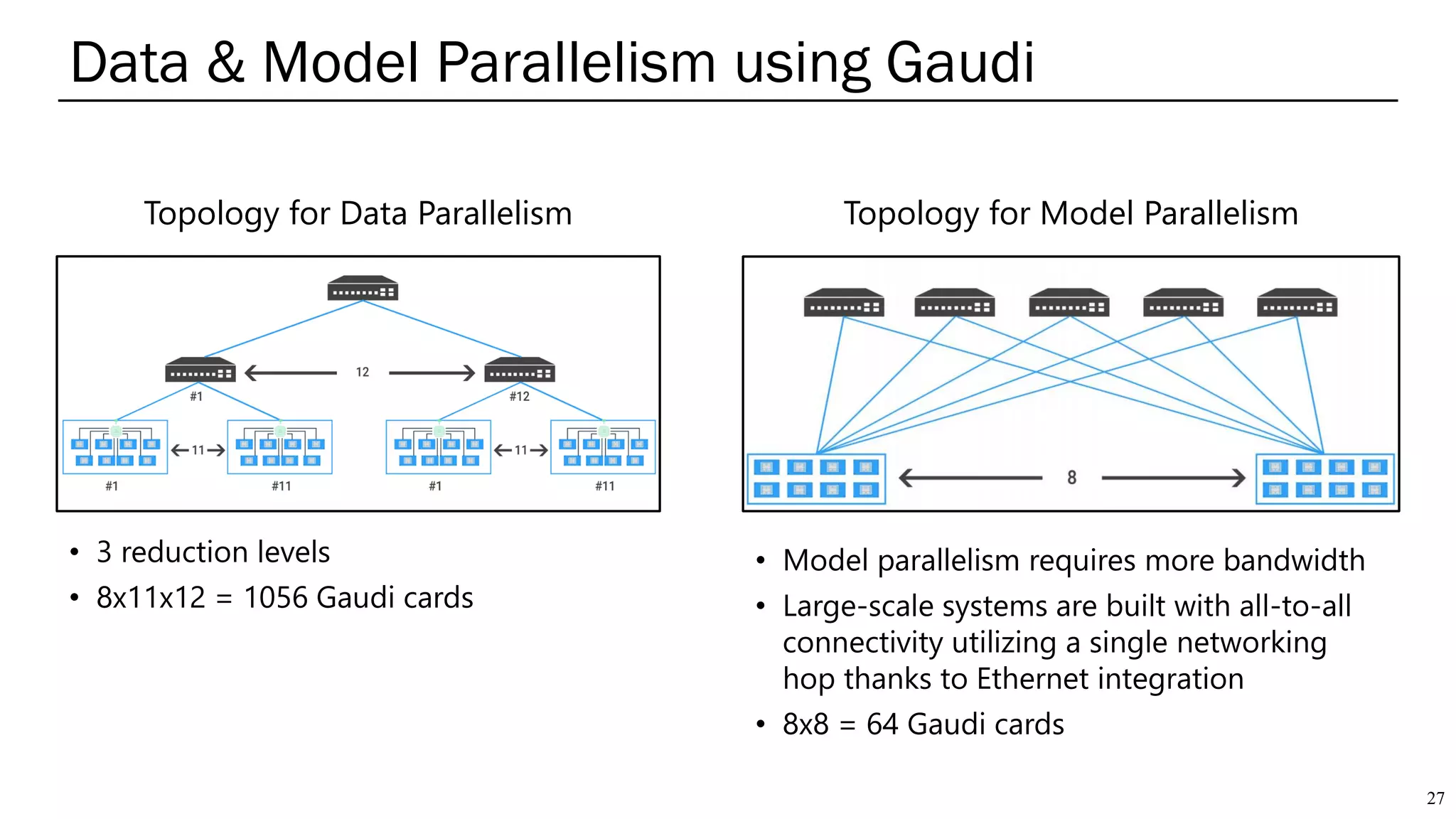
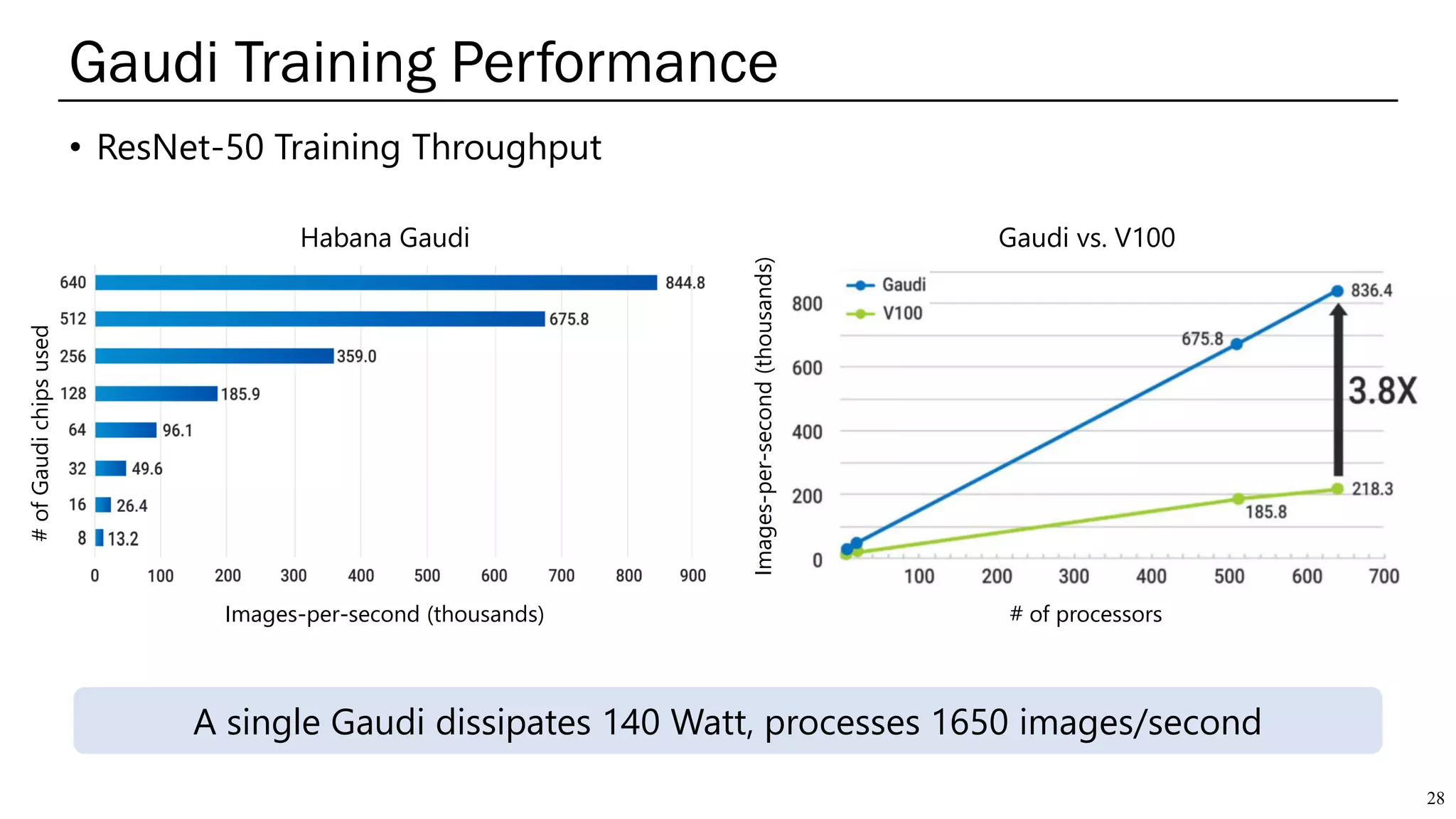
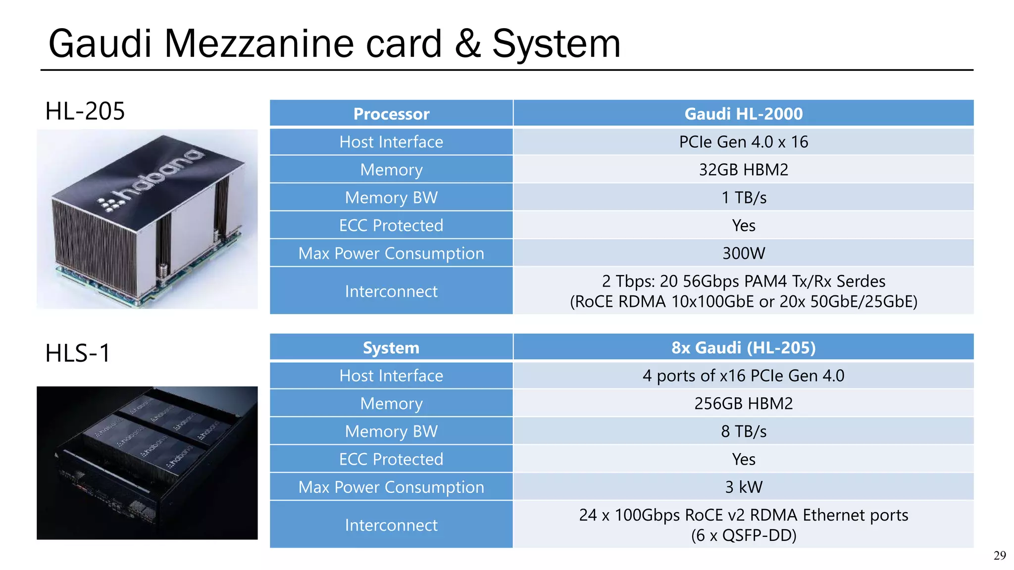
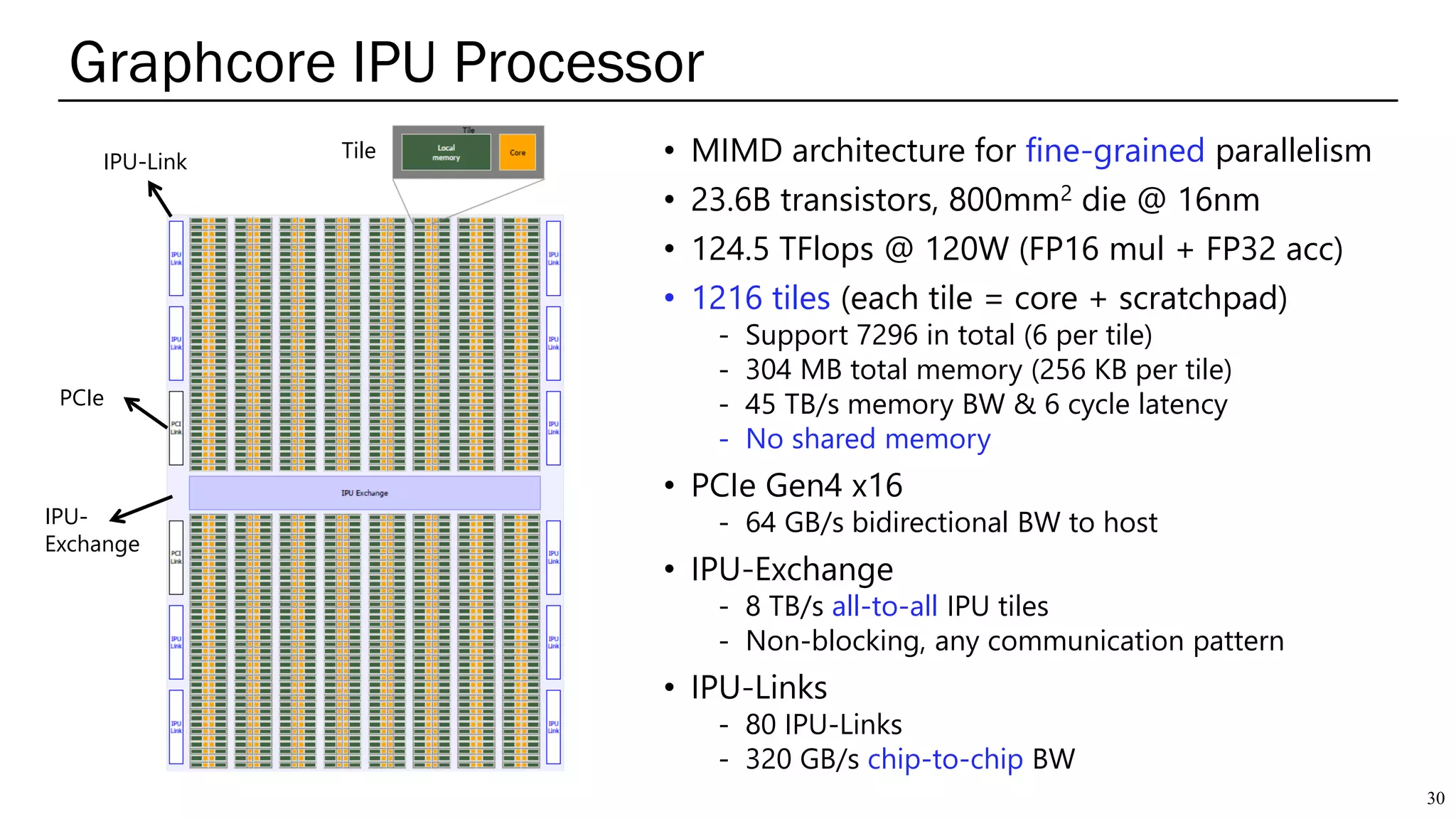
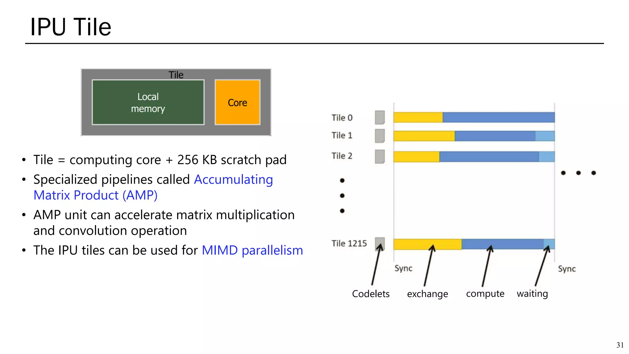
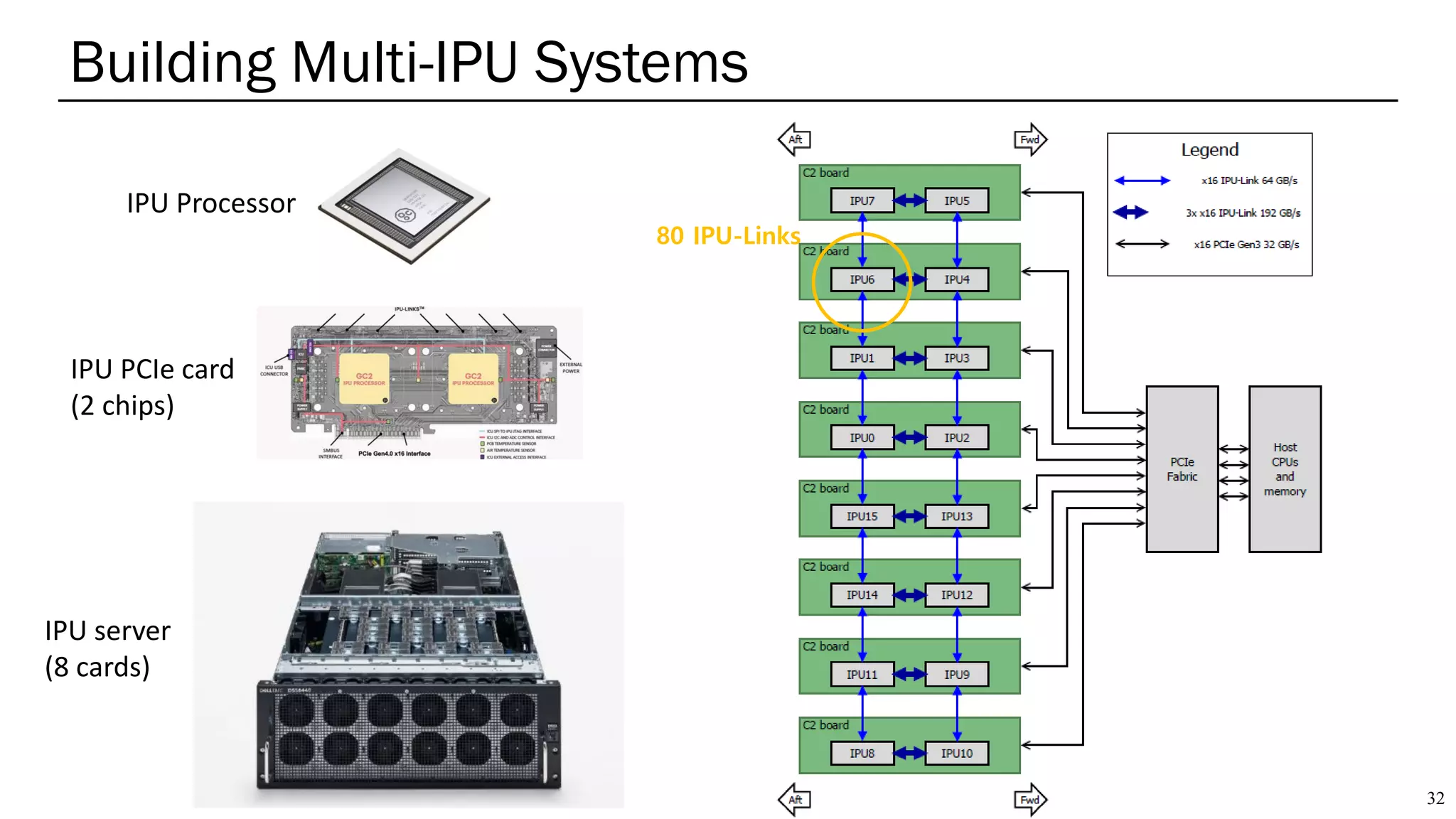
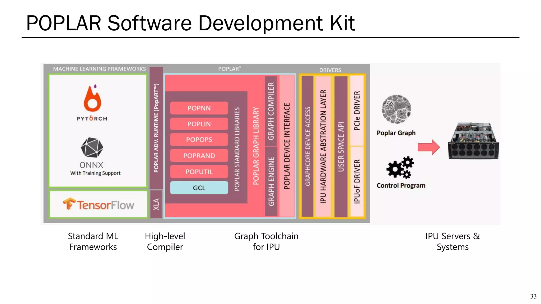
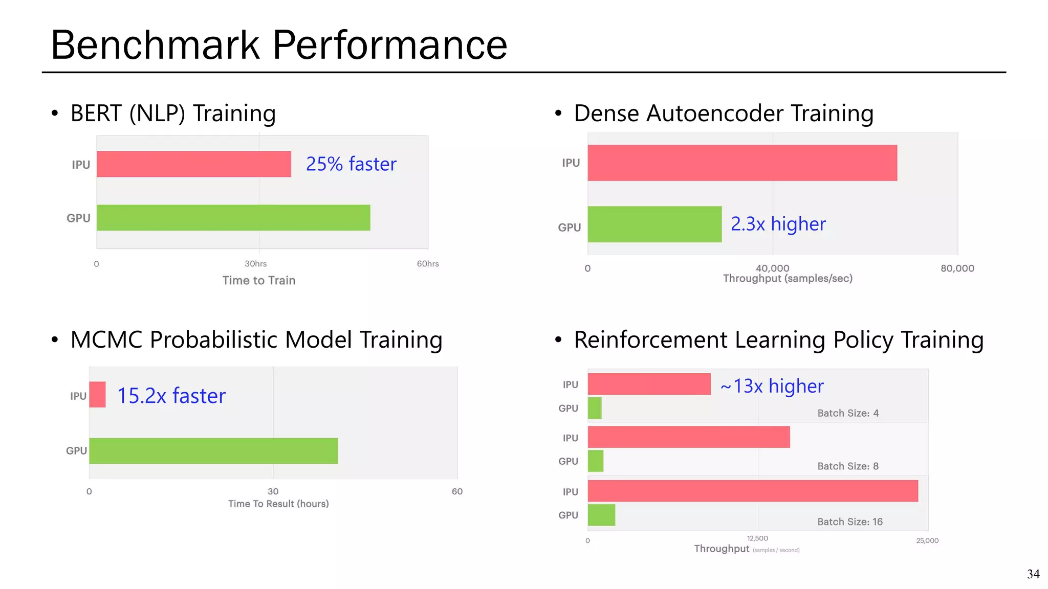
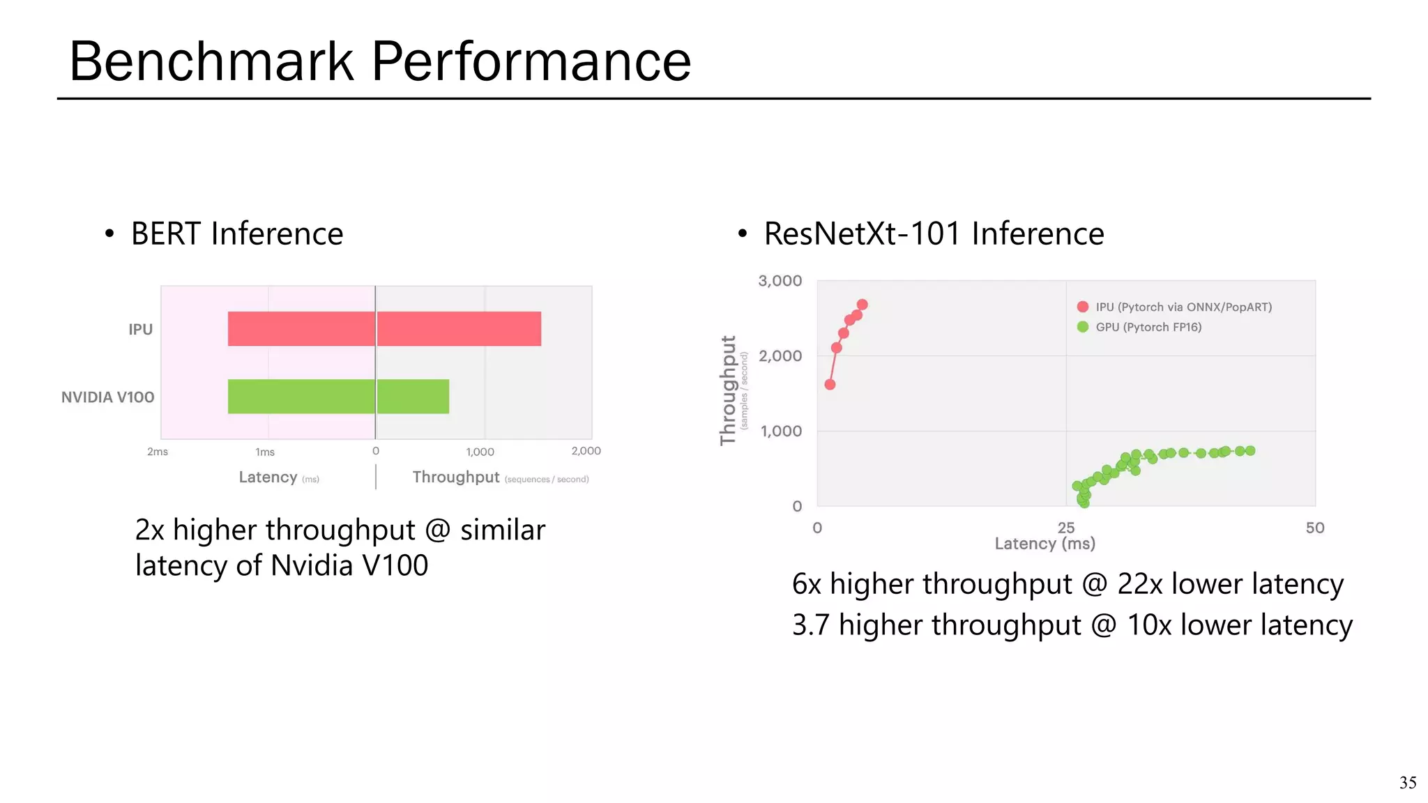
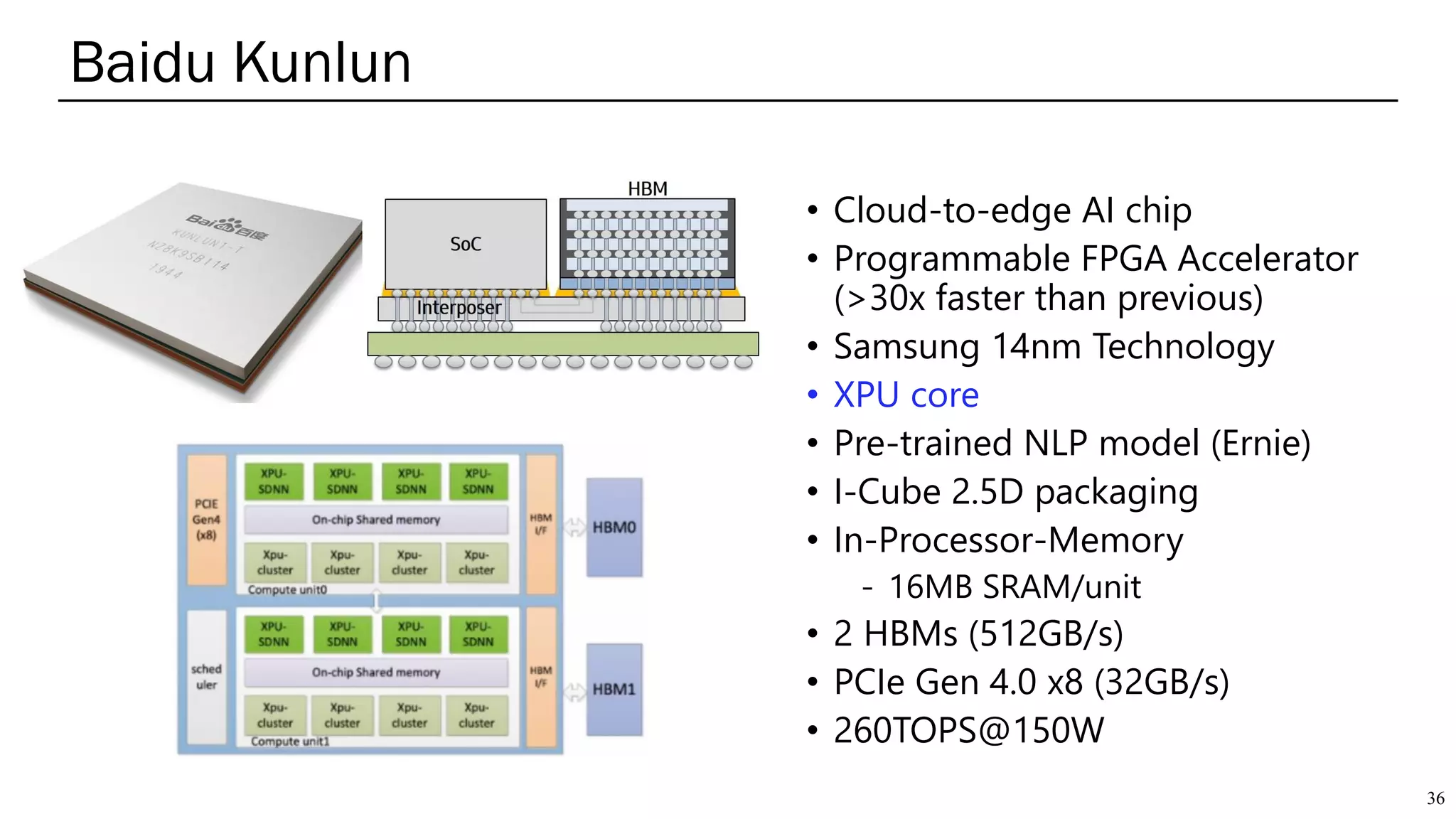
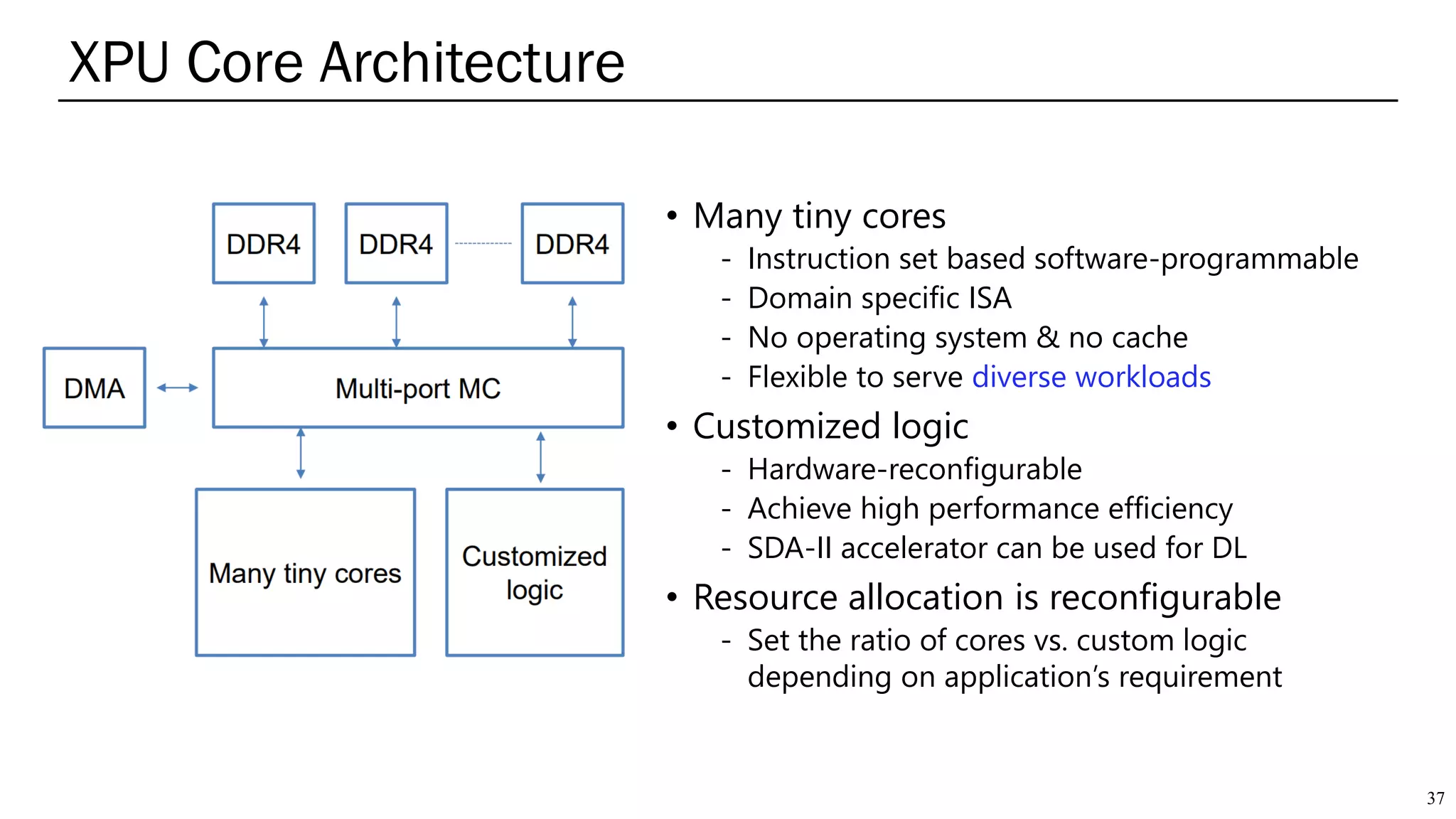
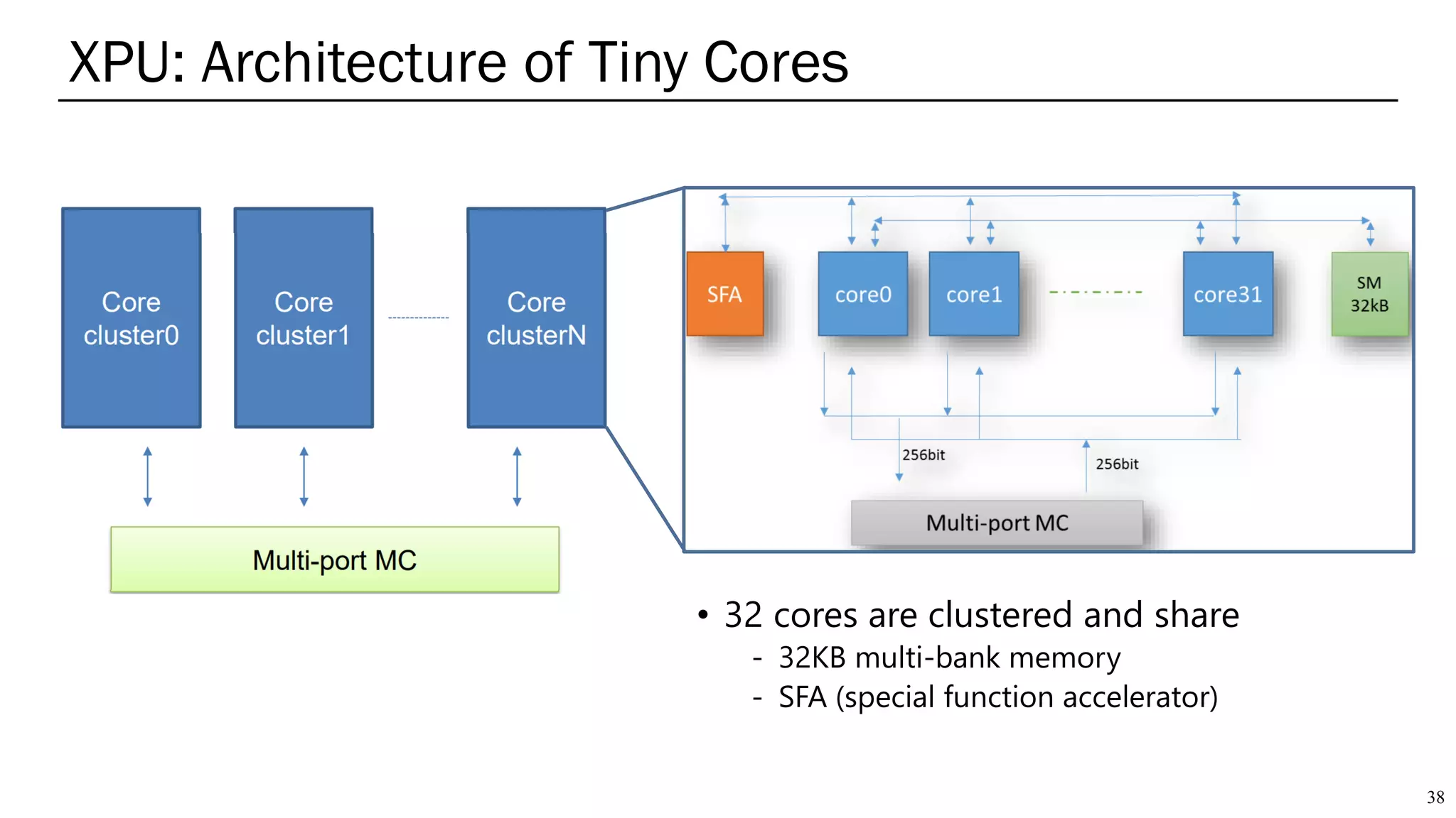
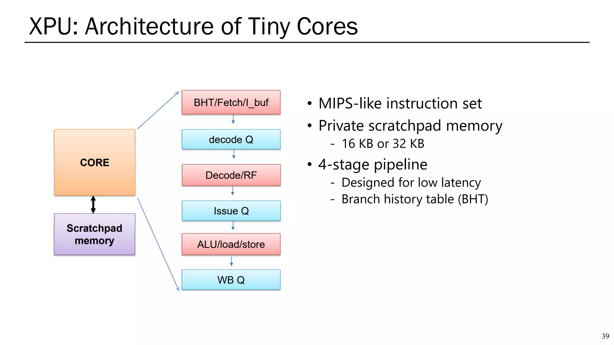
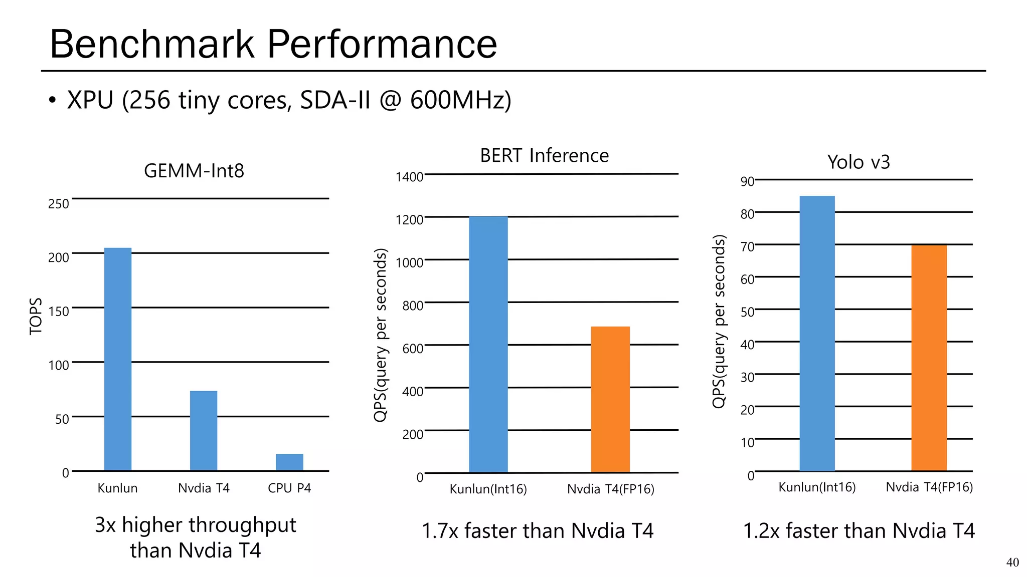
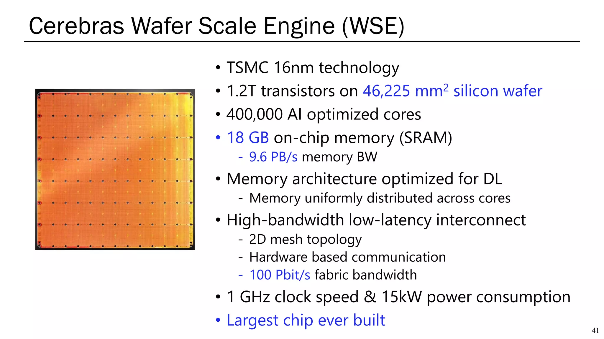
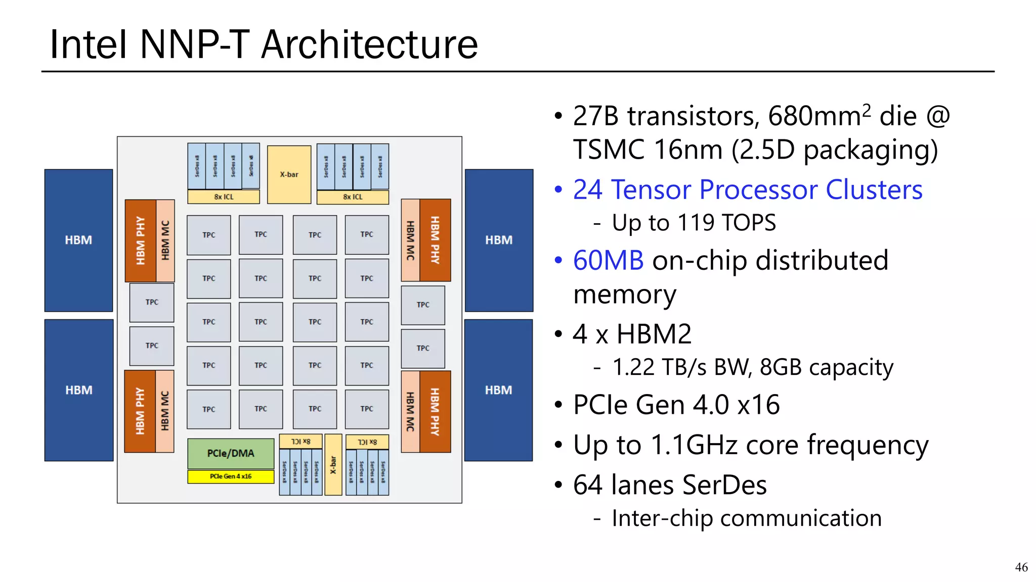
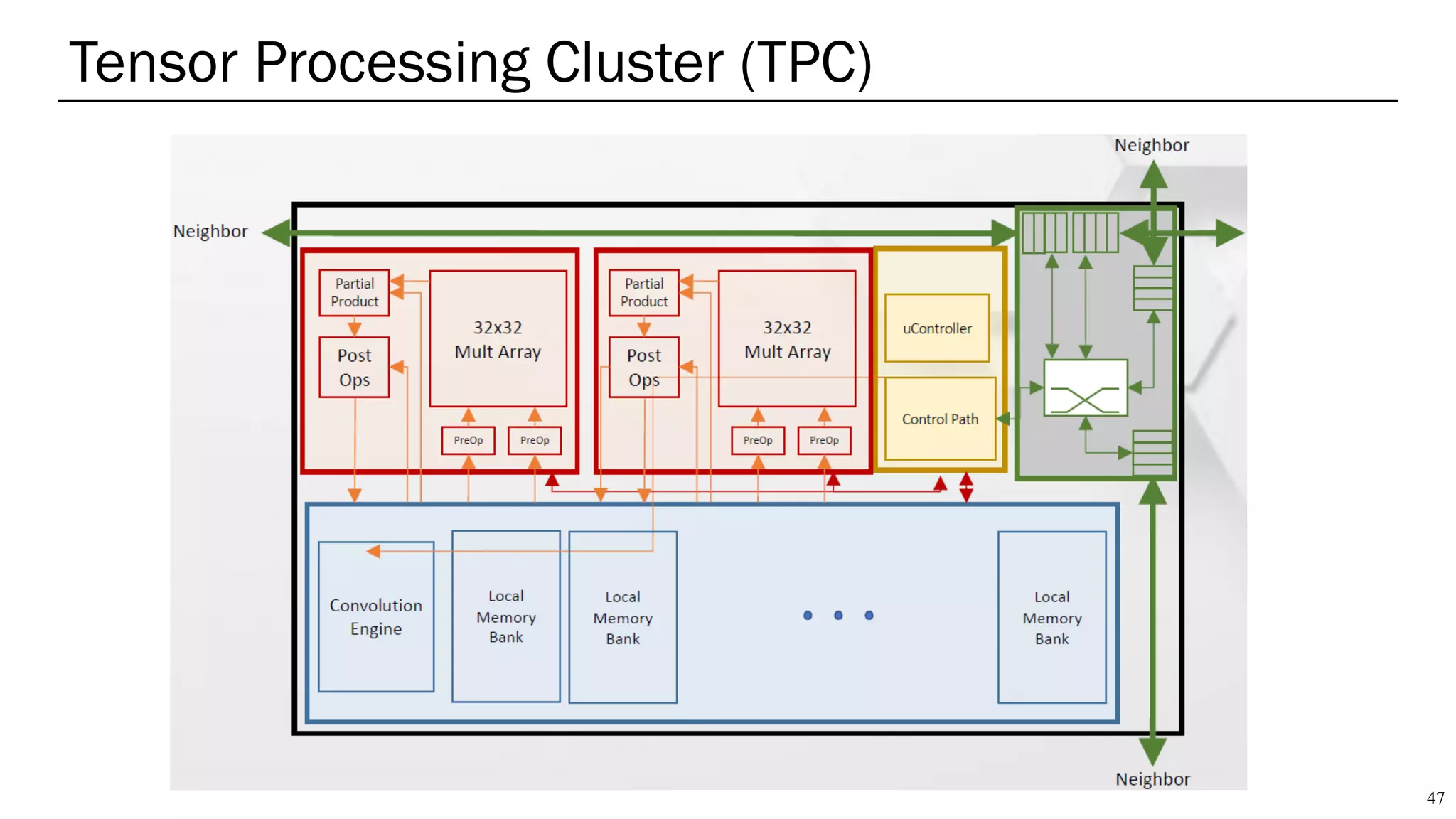
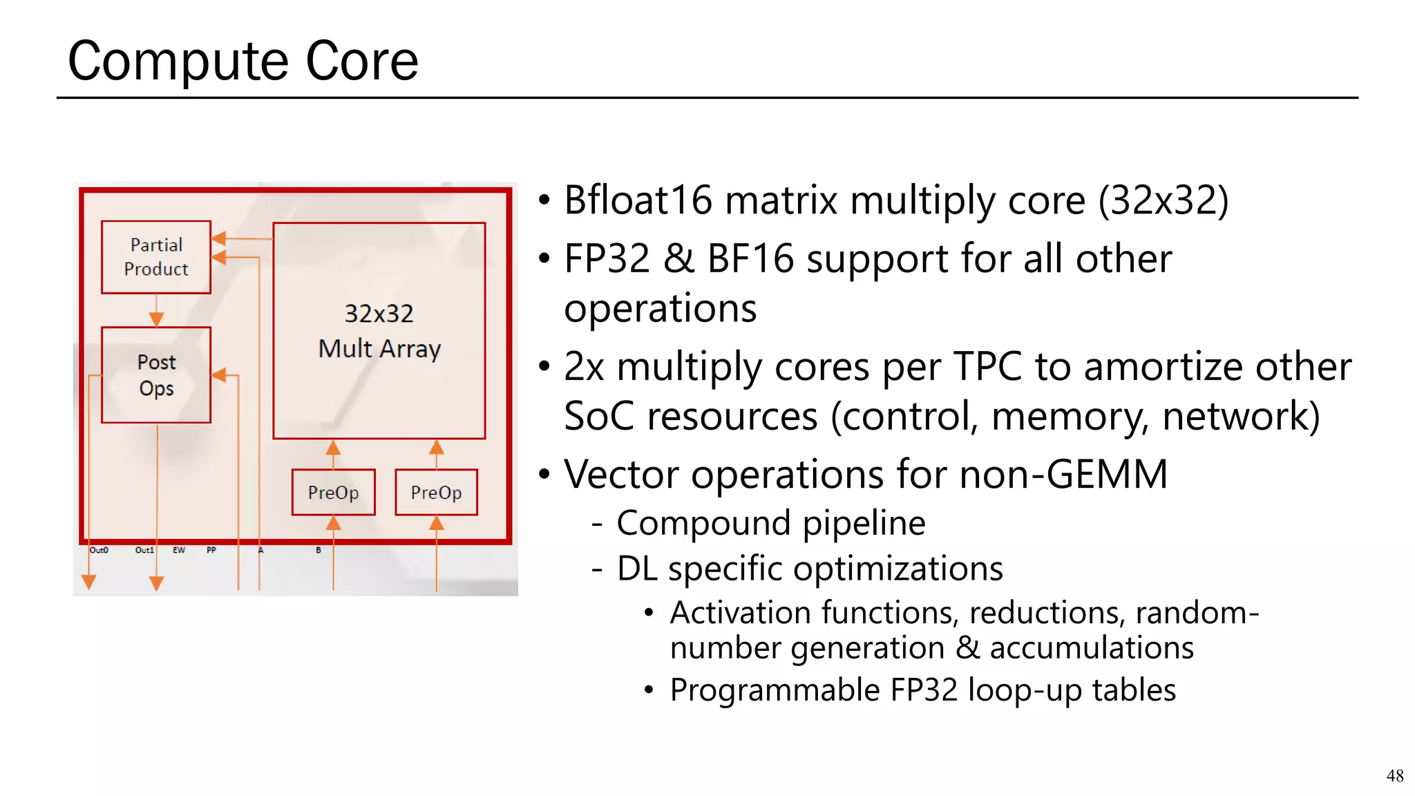
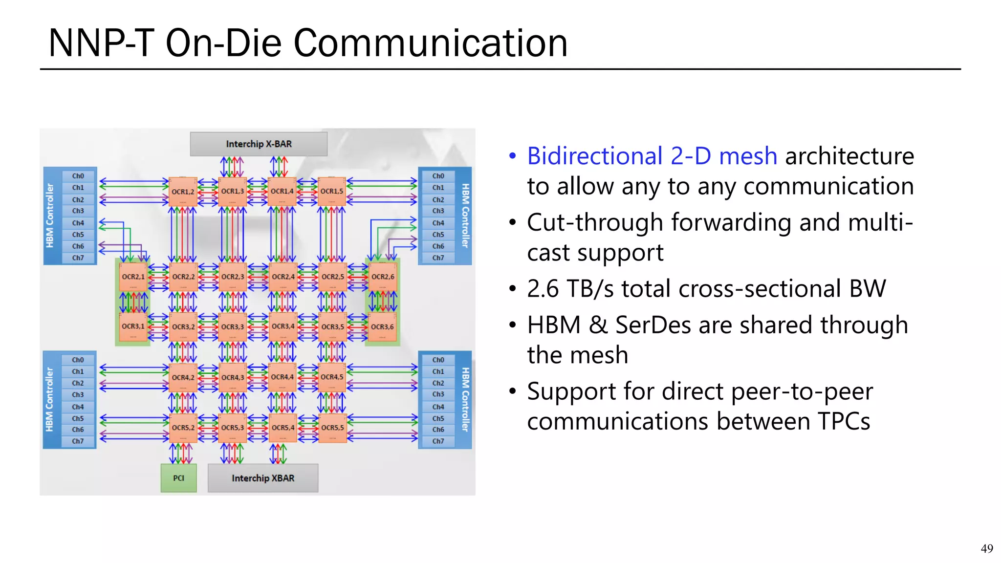
AI Accelerators for Cloud Datacenters
Prof. Joo-Young Kim
7/10/2020 @ 산업교육연구소
Agenda
2
• Introduction
• Cloud Infrastructure
- Datacenter challenges
- Microsoft Catapult
• AI Accelerators for Datacenters
- Google TPU
- HabanaLabs Gaudi
- Graphcore IPU
- Baidu Kunlun
- Cerebras Wafer-Scale Engine
- Intel NNP-T Processor
• Summary
Cloud Services
3
End of Moore’s Law
200+
Capabilities, Operating Cost Saving ∝ Performance/Watt per $
Energy Efficiency Trade-Off
4
Source: Bob Broderson, Berkeley Wireless group
Datacenter Challenges
• Workload diversity
Software services change monthly
Number of applications increases
• Maintenance
Little HW maintenance, no accessibility
Machines last ~3 years, can be repurposed during lifetime
Homogeneity is critical to reduce cost
• Specialization
Slowing of Moore’s law performance scaling
Compute requirements increase beyond conventional CPU-only systems
5
*Cycles in 50 hottest binaries (%)
*S. Kanev, “Profiling a Warehouse-Scale Computer,” ISCA 2015
FPGA vs ASIC
6
Xeon CPU NICSearch Acc.
(FPGA)
Search Acc.
(ASIC)
Wasted Power,
Holds back SW
Xeon CPU NICSearch Acc. v2
(FPGA)
NICXeon CPU Math
Accelerator
Wasted Power,
One more thing that
can break
Catapult Gen1 (2014)
• Altera Stratix V D5
• 172,600 ALMs, 2,014 M20Ks, 1,590 DSPs
• PCIe Gen 3 x8
• 8GB DDR3-1333
• Powered by PCIe slot
• 6x8 Torus Network
7
Stratix V
8GB DDR3
PCIe Gen3 x8
4 x 20Gbps
transceiver
“Reconfigurable Fabric for Accelerating Large-Scale Datacenter Services”, ISCA 2014
Open Compute Server
8
• Two 8-core Xeon 2.1 GHz CPUs
• 64 GB DRAM
• 4 HDDs @ 2 TB, 2 SSDs @ 512 GB
• 10 Gb Ethernet
• Plug-in FPGA via mezzanine connector
68 ⁰C
Mezz Conn.
Rack Design
9
• High density
- 1U (height:1.75inch), half-width servers
- Homogeneous design
- 1 FPGA per server, not enough for GPU
- Half rack: 2 x 24 servers
Server
Top Of Rack Switch (TOR)
Server
Server
Server
Server
Server
… …
D • Local Torus network
- Dedicated 6x8 torus enables multi-FPGA accelerators
- Requires additional cabling mapping physical 2x24 to
logical 6x8
Shell and Role
• Shell
- Operating system for FPGA
- Handles all I/O & management tasks
- Exposes simple FIFOs
• Role
- Only application logic
- Partial reconfiguration boundary
• Debug support
- Flight data recorder
- JTAG cable
10
West
SLIII
East
SLIII
South
SLIII
North
SLIII
x8 PCIe
Core
DMA
Engine
Config
Flash
(RSU)
DDR3 Core 1DDR3 Core 0
JTAG
LEDs
Temp
Sensors
Application
(Bing, Azure, DNN, etc.)
Shell
I2C
xcvr
reconfig
2 2 2 2
4 256 Mb
QSPI
Config
Flash
4 GB DDR3-
1333 ECC SO-
DIMM
4 GB DDR3-
1333 ECC SO-
DIMM
Host
CPU
72 72
Role
8
Inter-FPGA Router
SEU
Catapult Gen2 (2016)
11
• From Torus to Ethernet
- Bump-in-the-Wire (NIC FPGA Switch)
40G
NIC and TOR
FPGA
4GB DDR
2 x Gen3x8
PCIe
35W power budget
ToR
Switch
“A Cloud-Scale Acceleration Architecture,” Micro 2016
Integration to DC Infrastructure
12
…
A FPGA can communicate any FPGA in datacenter
Network Coverage and Latencies
13
0
5
10
15
20
25
1 10 100 1000 10000 100000 1000000
Round-TripLatency(us)
LTL L0 (same TOR)
LTL L1
Example L0 latency histogram
Example L1 latency histogram
Examples of L2 latency histograms for different pairs of FP
GAs
Number of Reachable Hosts/FPGAs
Catapult Gen1 Torus
(can reach up to 48 FPGAs)
LTL Average Laten
cyLTL 99.9th Percentile
6x8 Torus Latency
LTL L2
10K 100K 250K
Configurable Cloud
14
TOR TOR
L1
Storage
Deep neura
l networks
Web search
ranking
SQL
Web search
ranking
L2
TOR
L1
TOR
Bing Ranking Acceleration
15
99.9% SW latency
99.9% FPGA latency
Average FPGA query load Average SW load
Day 1 Day 2 Day 3 Day 4 Day 5
1.0
2.0
3.0
4.0
5.0
6.0
7.0
NormalizedLoad&Latency
• Lower latency than software even with 2x query load
• More consistent 99.9th tail latency
AI Chip Market
16
2000 2010 2020 2030
Deep Learning
Revolution
(AlexNet 2012)
Existing chips
GPU
AI Chip
> 1000
energy
efficiency
65B in 2025, 19% of semiconductor market, 18-19% growth per year
223 224
295
17 32
65
2017 2020E 2025E
93
88
81
7 11
19
2017 2020E 2025E
240 256
370
AI semiconductor
total market
($ billion)
AI semiconductor
total market
(%)
Non-AI AI
AI semiconductor
total market CAGR
2017-25, (%)
3-4
18-19
5x
Growth for AI Semiconductors
McKinsey report, 2019
RequiredperformanceforAI
AI Chip Industry
17
Google Facebook Microsoft Baidu Tesla HabanaLabs
TPUdeployment
(2016)
OpenCompute
initiative
(2011)
AIchipdevteam
(2019)
CatapultFPGA
deployment
(2014)
Brainwave
deployment
(2018)
Kunlun
inproduction
(2020)
FullSelfDriving
(FSD)chipfor
autonomous
vehicle(2019)
AItraining
processorGaudi
(2019)
And more (Graphcore, Cerabras, Intel, Groq, WaveComputing, ..)
Google TPU
• Simple architecture to support MLP, CNN, and
RNN models and have fast development
- Host interface
- Unified buffer (24 MB), weight FIFO
- Matrix multiply unit (256 x 256)
- Accumulators (256, 4 MB buffers)
- 8-bit integer multiplication
• Systolic array architecture
- Systolic execution saves energy by reducing reads
and writes of the Unified Buffer
- Activation data flows in from the left and weights
are pre-loaded from the top
- A given 256-element multiply-accumulate operation
moves through the matrix as a diagonal wavefront
- Throughput-oriented: control and data are pipelined
18
TPU v1 Performance
• CPU vs GPU vs TPU
19
Operational Intensity: MAC ops/weight byte
Teraops/sec
Google TPU
nVidia K80
Intel Haswell
GM: geometric mean, WM: weighted mean
TPU v2 & TPU v3
• 128 x 128 systolic array (22.5 TFLOPS per core)
• float32 accumulate / bfloat16 multiplies
• 2 cores + 2 HBMs per chip / 4 chips per board
20TPU v2 TPU v3
Cloud TPU v2 Pod
• Single board: 180TFLOPS + 64GB HBM
• Single pod (64 boards):11.5 PFLOPS + 4TB HBM
• 2D torus topology
21
Single board
Cloud TPU v3 Pod
• > 100 PFLOPS
• 32TB HBM
22
Habana Labs Gaudi
• Build for AI training performance at scale
- High throughput at low batch size
- High power efficiency
• Enable native Ethernet scale-out
- On-chip RDMA over Converged Ethernet (RoCE v2)
- Reduced system complexity, cost and power
- Leverage widely used standard Ethernet switches
• Promote standard form factors
- Open Compute Project Accelerator Module (OAM)
• SW infrastructure and tools
- Frameworks and ML compilers support
- TPC kernel library and user-friendly dev tools to enable
optimization/customization
23
Gaudi Processor Architecture
24
• 500mm2 die @ TSMC 16nm
• TPC 2.0 (Tensor Processing Core)
- Support DL training & inference
- VLIW SIMD (C-programmable)
• GEMM operation engine
- Highly configurable
• PCIe Gen4.0 x16
• 4 HBMs
- 2GT/s, 1TB/s BW, 32GB capacity
• RoCE v2
- 10 ports of 100Gb or 20 ports of 50Gb
• Mixed-precision data types
- FP32, BF16, INT32/16/8, UINT32/16/8
Heterogenous compute architecture
256GB/s, 8GB
per HBM
Gaudi Software Platform
25
Automatic floating-to-fixed quantization
with near-zero accuracy loss
User’s
custom
model
Host side
Device side
Training System with Gaudi
26
Various network configurations & systems possible for scale-out training
Habana Labs Systems-1 (HLS-1)
High-performance system with 16 Gaudi cards
Data & Model Parallelism using Gaudi
27
Topology for Data Parallelism Topology for Model Parallelism
• 3 reduction levels
• 8x11x12 = 1056 Gaudi cards
• Model parallelism requires more bandwidth
• Large-scale systems are built with all-to-all
connectivity utilizing a single networking
hop thanks to Ethernet integration
• 8x8 = 64 Gaudi cards
Gaudi Training Performance
28
• ResNet-50 Training Throughput
Images-per-second(thousands)
# of processors
Gaudi vs. V100
#ofGaudichipsused
Images-per-second (thousands)
Habana Gaudi
A single Gaudi dissipates 140 Watt, processes 1650 images/second
29
Processor Gaudi HL-2000
Host Interface PCIe Gen 4.0 x 16
Memory 32GB HBM2
Memory BW 1 TB/s
ECC Protected Yes
Max Power Consumption 300W
Interconnect
2 Tbps: 20 56Gbps PAM4 Tx/Rx Serdes
(RoCE RDMA 10x100GbE or 20x 50GbE/25GbE)
System 8x Gaudi (HL-205)
Host Interface 4 ports of x16 PCIe Gen 4.0
Memory 256GB HBM2
Memory BW 8 TB/s
ECC Protected Yes
Max Power Consumption 3 kW
Interconnect
24 x 100Gbps RoCE v2 RDMA Ethernet ports
(6 x QSFP-DD)
Gaudi Mezzanine card & System
HL-205
HLS-1
• MIMD architecture for fine-grained parallelism
• 23.6B transistors, 800mm2 die @ 16nm
• 124.5 TFlops @ 120W (FP16 mul + FP32 acc)
• 1216 tiles (each tile = core + scratchpad)
- Support 7296 in total (6 per tile)
- 304 MB total memory (256 KB per tile)
- 45 TB/s memory BW & 6 cycle latency
- No shared memory
• PCIe Gen4 x16
- 64 GB/s bidirectional BW to host
• IPU-Exchange
- 8 TB/s all-to-all IPU tiles
- Non-blocking, any communication pattern
• IPU-Links
- 80 IPU-Links
- 320 GB/s chip-to-chip BW
Graphcore IPU Processor
30
TileIPU-Link
PCIe
IPU-
Exchange
IPU Tile
31
• Tile = computing core + 256 KB scratch pad
• Specialized pipelines called Accumulating
Matrix Product (AMP)
• AMP unit can accelerate matrix multiplication
and convolution operation
• The IPU tiles can be used for MIMD parallelism
Codelets exchange compute waiting
Building Multi-IPU Systems
32
IPU Processor
IPU PCIe card
(2 chips)
IPU server
(8 cards)
80 IPU-Links
POPLAR Software Development Kit
33
Standard ML
Frameworks
Graph Toolchain
for IPU
IPU Servers &
Systems
High-level
Compiler
Benchmark Performance
34
• BERT (NLP) Training
25% faster
• Dense Autoencoder Training
2.3x higher
• MCMC Probabilistic Model Training
15.2x faster
• Reinforcement Learning Policy Training
~13x higher
Benchmark Performance
35
2x higher throughput @ similar
latency of Nvidia V100
• BERT Inference
6x higher throughput @ 22x lower latency
3.7 higher throughput @ 10x lower latency
• ResNetXt-101 Inference
Baidu Kunlun
36
• Cloud-to-edge AI chip
• Programmable FPGA Accelerator
(>30x faster than previous)
• Samsung 14nm Technology
• XPU core
• Pre-trained NLP model (Ernie)
• I-Cube 2.5D packaging
• In-Processor-Memory
- 16MB SRAM/unit
• 2 HBMs (512GB/s)
• PCIe Gen 4.0 x8 (32GB/s)
• 260TOPS@150W
XPU Core Architecture
37
• Many tiny cores
- Instruction set based software-programmable
- Domain specific ISA
- No operating system & no cache
- Flexible to serve diverse workloads
• Customized logic
- Hardware-reconfigurable
- Achieve high performance efficiency
- SDA-II accelerator can be used for DL
• Resource allocation is reconfigurable
- Set the ratio of cores vs. custom logic
depending on application’s requirement
XPU: Architecture of Tiny Cores
38
• 32 cores are clustered and share
- 32KB multi-bank memory
- SFA (special function accelerator)
XPU: Architecture of Tiny Cores
39
• MIPS-like instruction set
• Private scratchpad memory
- 16 KB or 32 KB
• 4-stage pipeline
- Designed for low latency
- Branch history table (BHT)
40
0
200
400
600
800
1000
Kunlun(Int16) Nvdia T4(FP16)
QPS(queryperseconds)
1200
1400
BERT Inference
3x higher throughput
than Nvdia T4
1.7x faster than Nvdia T4
0
50
100
150
200
250
GEMM-Int8
Kunlun Nvdia T4 CPU P4
TOPS
0
10
20
30
40
50
Kunlun(Int16) Nvdia T4(FP16)
QPS(queryperseconds)
70
80
60
90
Yolo v3
• XPU (256 tiny cores, SDA-II @ 600MHz)
Benchmark Performance
1.2x faster than Nvdia T4
• TSMC 16nm technology
• 1.2T transistors on 46,225 mm2 silicon wafer
• 400,000 AI optimized cores
• 18 GB on-chip memory (SRAM)
- 9.6 PB/s memory BW
• Memory architecture optimized for DL
- Memory uniformly distributed across cores
• High-bandwidth low-latency interconnect
- 2D mesh topology
- Hardware based communication
- 100 Pbit/s fabric bandwidth
• 1 GHz clock speed & 15kW power consumption
• Largest chip ever built
Cerebras Wafer Scale Engine (WSE)
41
• Fully programmable compute core
• Full array of general instructions with ML extensions
• Flexible general operations for control processing
- E.g. arithmetic, logical, load/store, branch
• Optimized for tensor operations
- Tensors as first class operands
• Sparsity harvesting technology
- SLA cores intelligently skip the zeros
- All zeros are filtered out
Cerebras Wafer Scale Engine Core
42
Sparse Linear Algebra (SLA) Core
• Neural network(NN) models expressed in common ML frameworks
• Cerebras interface to framework extracts the NN
• Performs placement and routing to map NN layers to fabric
• The entire wafer operates on the single neural network
Programming the Wafer Scale Engine
43
44
Challenges of WSE
• Cross die connectivity
- Add cross-die wires across scribe lines of wafer in partnership with TSMC
• Yield
- Have redundant cores and reconnect fabric
• Wafer-wide package assembly technology
• Power and cooling
Intel NNP-T
45
• Intel Nervana Neural Network Processor
for Training (NNP-T)
• Train a network as fast as possible within
a given power budget, targeting larger
models and datasets
• Balance between compute, communication,
and memory for system performance
• Reuse on-die data as much as possible
• Optimize for batched workloads
• Build-in scale-out support
Intel NNP-T Architecture
46
• 27B transistors, 680mm2 die @
TSMC 16nm (2.5D packaging)
• 24 Tensor Processor Clusters
- Up to 119 TOPS
• 60MB on-chip distributed
memory
• 4 x HBM2
- 1.22 TB/s BW, 8GB capacity
• PCIe Gen 4.0 x16
• Up to 1.1GHz core frequency
• 64 lanes SerDes
- Inter-chip communication
Tensor Processing Cluster (TPC)
47
Compute Core
48
• Bfloat16 matrix multiply core (32x32)
• FP32 & BF16 support for all other
operations
• 2x multiply cores per TPC to amortize other
SoC resources (control, memory, network)
• Vector operations for non-GEMM
- Compound pipeline
- DL specific optimizations
• Activation functions, reductions, random-
number generation & accumulations
• Programmable FP32 loop-up tables
• Bidirectional 2-D mesh architecture
to allow any to any communication
• Cut-through forwarding and multi-
cast support
• 2.6 TB/s total cross-sectional BW
• HBM & SerDes are shared through
the mesh
• Support for direct peer-to-peer
communications between TPCs
NNP-T On-Die Communication
49
• Full software stack built with open components
• Direct integration with DL frameworks
• nGraph
- Hardware agnostic DL library & compiler
- Provides common set of optimizations for NNP-T
• Argon
- NNP-T DNN compute & communication kernel
library
• Low-level programmability
- NNP-T kernel development toolchain w/ tensor
compiler
NNP-T Software Stack
50
Argon
DNN Kernel Library
Kernel Mode Driver
Board Firmware Chip Firmware
Benchmark Performance
51
Description Utilization
c64xh56xw56_k64xr3xs3_st1_n128 86%
c128xh28xw28_k128xr3xs3_st1_n128 71%
c512xh28xw28_k128xr1xs1_st1_n128 65%
c128xh28xw28_k512xr1xs1_st1_n128 59%
c256xh14xw14_k1024xr1xs1_st1_n128 62%
c256xh28xw28_k512xr1xs1_st2_n128 71%
c32xh120xw120_k64xr5xs5_st1_n128 87%
C=# input dimensions, H=height, W=width, K=# filters,
R=filter X, S=filter Y, ST=stride N=minibatch size
GEMM Size Utilization
1024 x 700 x 512 31.1%
1760 x 7133 x 1760 44.5%
2048 x 7133 x 2048 46.7%
2560 x 7133 x 2560 57.1%
4096 x 7133 x 4096 57.4%
5124 x 9124 x 2048 55.5%
Convolution operationGEMM operation
Summary
52
• Cloud AI accelerators’ goals
- High cost-performance over GPU, scalability, programmability
• Compute
- Specialized cores for tensor processing such as matrix, convolution
• Memory
- HBM
- Distributed on-chip memory & scratchpads
- No hardware caches
• Communications
- High bandwidth on-chip networks
- Custom inter-chip links
- PCIe Gen 4.0 to host
• Software
- Compatibility to existing frameworks (ONNX, TensorFlow, PyTorch)
- Graph compiler + device-oriented optimization
References
53
- https://www.hotchips.org/hc31/HC31_1.14_HabanaLabs.Eitan_Medina.v9.pdf
- https://habana.ai/wp-content/uploads/2019/06/Habana-Gaudi-Training-Platform-whitepaper.pdf
- https://www.graphcore.ai/products/ipu
- https://www.servethehome.com/hands-on-with-a-graphcore-c2-ipu-pcie-card-at-dell-tech-world/
- Z. Jia, “Dissecting the Graphcore IPU Architecture via Microbenchmarking,” Citadel technical report, 2019
- V. Rege, “Graphcore, the Need for New Hardware for Artificial Intelligence,” AI Hardware Summit 2019
- https://www.graphcore.ai/posts/new-graphcore-ipu-benchmarks
- https://m.itbiznews.com/news/newsview.php?ncode=1065569594387854
- https://www.hotchips.org/wp-content/uploads/hc_archives/hc29/HC29.21-Monday-Pub/HC29.21.40-
Processors-Pub/HC29.21.410-XPU-FPGA-Ouyang-Baidu.pdf
- https://www.firstxw.com/view/254356.html
- https://www.hotchips.org/hc31/HC31_1.13_Cerebras.SeanLie.v02.pdf
- https://www.cerebras.net/cerebras-wafer-scale-engine-why-we-need-big-chips-for-deep-learning/
- https://www.hotchips.org/hc31/HC31_1.12_Intel_Intel.AndrewYang.v0.92.pdf
- https://www.businesswire.com/news/home/20191112005277/en/Intel-Speeds-AI-Development-
Deployment-Performance-New

AI Accelerators for Cloud Datacenters

  • 1.
    AI Accelerators forCloud Datacenters Prof. Joo-Young Kim 7/10/2020 @ 산업교육연구소
  • 2.
    Agenda 2 • Introduction • CloudInfrastructure - Datacenter challenges - Microsoft Catapult • AI Accelerators for Datacenters - Google TPU - HabanaLabs Gaudi - Graphcore IPU - Baidu Kunlun - Cerebras Wafer-Scale Engine - Intel NNP-T Processor • Summary
  • 3.
    Cloud Services 3 End ofMoore’s Law 200+ Capabilities, Operating Cost Saving ∝ Performance/Watt per $
  • 4.
    Energy Efficiency Trade-Off 4 Source:Bob Broderson, Berkeley Wireless group
  • 5.
    Datacenter Challenges • Workloaddiversity Software services change monthly Number of applications increases • Maintenance Little HW maintenance, no accessibility Machines last ~3 years, can be repurposed during lifetime Homogeneity is critical to reduce cost • Specialization Slowing of Moore’s law performance scaling Compute requirements increase beyond conventional CPU-only systems 5 *Cycles in 50 hottest binaries (%) *S. Kanev, “Profiling a Warehouse-Scale Computer,” ISCA 2015
  • 6.
    FPGA vs ASIC 6 XeonCPU NICSearch Acc. (FPGA) Search Acc. (ASIC) Wasted Power, Holds back SW Xeon CPU NICSearch Acc. v2 (FPGA) NICXeon CPU Math Accelerator Wasted Power, One more thing that can break
  • 7.
    Catapult Gen1 (2014) •Altera Stratix V D5 • 172,600 ALMs, 2,014 M20Ks, 1,590 DSPs • PCIe Gen 3 x8 • 8GB DDR3-1333 • Powered by PCIe slot • 6x8 Torus Network 7 Stratix V 8GB DDR3 PCIe Gen3 x8 4 x 20Gbps transceiver “Reconfigurable Fabric for Accelerating Large-Scale Datacenter Services”, ISCA 2014
  • 8.
    Open Compute Server 8 •Two 8-core Xeon 2.1 GHz CPUs • 64 GB DRAM • 4 HDDs @ 2 TB, 2 SSDs @ 512 GB • 10 Gb Ethernet • Plug-in FPGA via mezzanine connector 68 ⁰C Mezz Conn.
  • 9.
    Rack Design 9 • Highdensity - 1U (height:1.75inch), half-width servers - Homogeneous design - 1 FPGA per server, not enough for GPU - Half rack: 2 x 24 servers Server Top Of Rack Switch (TOR) Server Server Server Server Server … … D • Local Torus network - Dedicated 6x8 torus enables multi-FPGA accelerators - Requires additional cabling mapping physical 2x24 to logical 6x8
  • 10.
    Shell and Role •Shell - Operating system for FPGA - Handles all I/O & management tasks - Exposes simple FIFOs • Role - Only application logic - Partial reconfiguration boundary • Debug support - Flight data recorder - JTAG cable 10 West SLIII East SLIII South SLIII North SLIII x8 PCIe Core DMA Engine Config Flash (RSU) DDR3 Core 1DDR3 Core 0 JTAG LEDs Temp Sensors Application (Bing, Azure, DNN, etc.) Shell I2C xcvr reconfig 2 2 2 2 4 256 Mb QSPI Config Flash 4 GB DDR3- 1333 ECC SO- DIMM 4 GB DDR3- 1333 ECC SO- DIMM Host CPU 72 72 Role 8 Inter-FPGA Router SEU
  • 11.
    Catapult Gen2 (2016) 11 •From Torus to Ethernet - Bump-in-the-Wire (NIC FPGA Switch) 40G NIC and TOR FPGA 4GB DDR 2 x Gen3x8 PCIe 35W power budget ToR Switch “A Cloud-Scale Acceleration Architecture,” Micro 2016
  • 12.
    Integration to DCInfrastructure 12 … A FPGA can communicate any FPGA in datacenter
  • 13.
    Network Coverage andLatencies 13 0 5 10 15 20 25 1 10 100 1000 10000 100000 1000000 Round-TripLatency(us) LTL L0 (same TOR) LTL L1 Example L0 latency histogram Example L1 latency histogram Examples of L2 latency histograms for different pairs of FP GAs Number of Reachable Hosts/FPGAs Catapult Gen1 Torus (can reach up to 48 FPGAs) LTL Average Laten cyLTL 99.9th Percentile 6x8 Torus Latency LTL L2 10K 100K 250K
  • 14.
    Configurable Cloud 14 TOR TOR L1 Storage Deepneura l networks Web search ranking SQL Web search ranking L2 TOR L1 TOR
  • 15.
    Bing Ranking Acceleration 15 99.9%SW latency 99.9% FPGA latency Average FPGA query load Average SW load Day 1 Day 2 Day 3 Day 4 Day 5 1.0 2.0 3.0 4.0 5.0 6.0 7.0 NormalizedLoad&Latency • Lower latency than software even with 2x query load • More consistent 99.9th tail latency
  • 16.
    AI Chip Market 16 20002010 2020 2030 Deep Learning Revolution (AlexNet 2012) Existing chips GPU AI Chip > 1000 energy efficiency 65B in 2025, 19% of semiconductor market, 18-19% growth per year 223 224 295 17 32 65 2017 2020E 2025E 93 88 81 7 11 19 2017 2020E 2025E 240 256 370 AI semiconductor total market ($ billion) AI semiconductor total market (%) Non-AI AI AI semiconductor total market CAGR 2017-25, (%) 3-4 18-19 5x Growth for AI Semiconductors McKinsey report, 2019 RequiredperformanceforAI
  • 17.
    AI Chip Industry 17 GoogleFacebook Microsoft Baidu Tesla HabanaLabs TPUdeployment (2016) OpenCompute initiative (2011) AIchipdevteam (2019) CatapultFPGA deployment (2014) Brainwave deployment (2018) Kunlun inproduction (2020) FullSelfDriving (FSD)chipfor autonomous vehicle(2019) AItraining processorGaudi (2019) And more (Graphcore, Cerabras, Intel, Groq, WaveComputing, ..)
  • 18.
    Google TPU • Simplearchitecture to support MLP, CNN, and RNN models and have fast development - Host interface - Unified buffer (24 MB), weight FIFO - Matrix multiply unit (256 x 256) - Accumulators (256, 4 MB buffers) - 8-bit integer multiplication • Systolic array architecture - Systolic execution saves energy by reducing reads and writes of the Unified Buffer - Activation data flows in from the left and weights are pre-loaded from the top - A given 256-element multiply-accumulate operation moves through the matrix as a diagonal wavefront - Throughput-oriented: control and data are pipelined 18
  • 19.
    TPU v1 Performance •CPU vs GPU vs TPU 19 Operational Intensity: MAC ops/weight byte Teraops/sec Google TPU nVidia K80 Intel Haswell GM: geometric mean, WM: weighted mean
  • 20.
    TPU v2 &TPU v3 • 128 x 128 systolic array (22.5 TFLOPS per core) • float32 accumulate / bfloat16 multiplies • 2 cores + 2 HBMs per chip / 4 chips per board 20TPU v2 TPU v3
  • 21.
    Cloud TPU v2Pod • Single board: 180TFLOPS + 64GB HBM • Single pod (64 boards):11.5 PFLOPS + 4TB HBM • 2D torus topology 21 Single board
  • 22.
    Cloud TPU v3Pod • > 100 PFLOPS • 32TB HBM 22
  • 23.
    Habana Labs Gaudi •Build for AI training performance at scale - High throughput at low batch size - High power efficiency • Enable native Ethernet scale-out - On-chip RDMA over Converged Ethernet (RoCE v2) - Reduced system complexity, cost and power - Leverage widely used standard Ethernet switches • Promote standard form factors - Open Compute Project Accelerator Module (OAM) • SW infrastructure and tools - Frameworks and ML compilers support - TPC kernel library and user-friendly dev tools to enable optimization/customization 23
  • 24.
    Gaudi Processor Architecture 24 •500mm2 die @ TSMC 16nm • TPC 2.0 (Tensor Processing Core) - Support DL training & inference - VLIW SIMD (C-programmable) • GEMM operation engine - Highly configurable • PCIe Gen4.0 x16 • 4 HBMs - 2GT/s, 1TB/s BW, 32GB capacity • RoCE v2 - 10 ports of 100Gb or 20 ports of 50Gb • Mixed-precision data types - FP32, BF16, INT32/16/8, UINT32/16/8 Heterogenous compute architecture 256GB/s, 8GB per HBM
  • 25.
    Gaudi Software Platform 25 Automaticfloating-to-fixed quantization with near-zero accuracy loss User’s custom model Host side Device side
  • 26.
    Training System withGaudi 26 Various network configurations & systems possible for scale-out training Habana Labs Systems-1 (HLS-1) High-performance system with 16 Gaudi cards
  • 27.
    Data & ModelParallelism using Gaudi 27 Topology for Data Parallelism Topology for Model Parallelism • 3 reduction levels • 8x11x12 = 1056 Gaudi cards • Model parallelism requires more bandwidth • Large-scale systems are built with all-to-all connectivity utilizing a single networking hop thanks to Ethernet integration • 8x8 = 64 Gaudi cards
  • 28.
    Gaudi Training Performance 28 •ResNet-50 Training Throughput Images-per-second(thousands) # of processors Gaudi vs. V100 #ofGaudichipsused Images-per-second (thousands) Habana Gaudi A single Gaudi dissipates 140 Watt, processes 1650 images/second
  • 29.
    29 Processor Gaudi HL-2000 HostInterface PCIe Gen 4.0 x 16 Memory 32GB HBM2 Memory BW 1 TB/s ECC Protected Yes Max Power Consumption 300W Interconnect 2 Tbps: 20 56Gbps PAM4 Tx/Rx Serdes (RoCE RDMA 10x100GbE or 20x 50GbE/25GbE) System 8x Gaudi (HL-205) Host Interface 4 ports of x16 PCIe Gen 4.0 Memory 256GB HBM2 Memory BW 8 TB/s ECC Protected Yes Max Power Consumption 3 kW Interconnect 24 x 100Gbps RoCE v2 RDMA Ethernet ports (6 x QSFP-DD) Gaudi Mezzanine card & System HL-205 HLS-1
  • 30.
    • MIMD architecturefor fine-grained parallelism • 23.6B transistors, 800mm2 die @ 16nm • 124.5 TFlops @ 120W (FP16 mul + FP32 acc) • 1216 tiles (each tile = core + scratchpad) - Support 7296 in total (6 per tile) - 304 MB total memory (256 KB per tile) - 45 TB/s memory BW & 6 cycle latency - No shared memory • PCIe Gen4 x16 - 64 GB/s bidirectional BW to host • IPU-Exchange - 8 TB/s all-to-all IPU tiles - Non-blocking, any communication pattern • IPU-Links - 80 IPU-Links - 320 GB/s chip-to-chip BW Graphcore IPU Processor 30 TileIPU-Link PCIe IPU- Exchange
  • 31.
    IPU Tile 31 • Tile= computing core + 256 KB scratch pad • Specialized pipelines called Accumulating Matrix Product (AMP) • AMP unit can accelerate matrix multiplication and convolution operation • The IPU tiles can be used for MIMD parallelism Codelets exchange compute waiting
  • 32.
    Building Multi-IPU Systems 32 IPUProcessor IPU PCIe card (2 chips) IPU server (8 cards) 80 IPU-Links
  • 33.
    POPLAR Software DevelopmentKit 33 Standard ML Frameworks Graph Toolchain for IPU IPU Servers & Systems High-level Compiler
  • 34.
    Benchmark Performance 34 • BERT(NLP) Training 25% faster • Dense Autoencoder Training 2.3x higher • MCMC Probabilistic Model Training 15.2x faster • Reinforcement Learning Policy Training ~13x higher
  • 35.
    Benchmark Performance 35 2x higherthroughput @ similar latency of Nvidia V100 • BERT Inference 6x higher throughput @ 22x lower latency 3.7 higher throughput @ 10x lower latency • ResNetXt-101 Inference
  • 36.
    Baidu Kunlun 36 • Cloud-to-edgeAI chip • Programmable FPGA Accelerator (>30x faster than previous) • Samsung 14nm Technology • XPU core • Pre-trained NLP model (Ernie) • I-Cube 2.5D packaging • In-Processor-Memory - 16MB SRAM/unit • 2 HBMs (512GB/s) • PCIe Gen 4.0 x8 (32GB/s) • 260TOPS@150W
  • 37.
    XPU Core Architecture 37 •Many tiny cores - Instruction set based software-programmable - Domain specific ISA - No operating system & no cache - Flexible to serve diverse workloads • Customized logic - Hardware-reconfigurable - Achieve high performance efficiency - SDA-II accelerator can be used for DL • Resource allocation is reconfigurable - Set the ratio of cores vs. custom logic depending on application’s requirement
  • 38.
    XPU: Architecture ofTiny Cores 38 • 32 cores are clustered and share - 32KB multi-bank memory - SFA (special function accelerator)
  • 39.
    XPU: Architecture ofTiny Cores 39 • MIPS-like instruction set • Private scratchpad memory - 16 KB or 32 KB • 4-stage pipeline - Designed for low latency - Branch history table (BHT)
  • 40.
    40 0 200 400 600 800 1000 Kunlun(Int16) Nvdia T4(FP16) QPS(queryperseconds) 1200 1400 BERTInference 3x higher throughput than Nvdia T4 1.7x faster than Nvdia T4 0 50 100 150 200 250 GEMM-Int8 Kunlun Nvdia T4 CPU P4 TOPS 0 10 20 30 40 50 Kunlun(Int16) Nvdia T4(FP16) QPS(queryperseconds) 70 80 60 90 Yolo v3 • XPU (256 tiny cores, SDA-II @ 600MHz) Benchmark Performance 1.2x faster than Nvdia T4
  • 41.
    • TSMC 16nmtechnology • 1.2T transistors on 46,225 mm2 silicon wafer • 400,000 AI optimized cores • 18 GB on-chip memory (SRAM) - 9.6 PB/s memory BW • Memory architecture optimized for DL - Memory uniformly distributed across cores • High-bandwidth low-latency interconnect - 2D mesh topology - Hardware based communication - 100 Pbit/s fabric bandwidth • 1 GHz clock speed & 15kW power consumption • Largest chip ever built Cerebras Wafer Scale Engine (WSE) 41
  • 42.
    • Fully programmablecompute core • Full array of general instructions with ML extensions • Flexible general operations for control processing - E.g. arithmetic, logical, load/store, branch • Optimized for tensor operations - Tensors as first class operands • Sparsity harvesting technology - SLA cores intelligently skip the zeros - All zeros are filtered out Cerebras Wafer Scale Engine Core 42 Sparse Linear Algebra (SLA) Core
  • 43.
    • Neural network(NN)models expressed in common ML frameworks • Cerebras interface to framework extracts the NN • Performs placement and routing to map NN layers to fabric • The entire wafer operates on the single neural network Programming the Wafer Scale Engine 43
  • 44.
    44 Challenges of WSE •Cross die connectivity - Add cross-die wires across scribe lines of wafer in partnership with TSMC • Yield - Have redundant cores and reconnect fabric • Wafer-wide package assembly technology • Power and cooling
  • 45.
    Intel NNP-T 45 • IntelNervana Neural Network Processor for Training (NNP-T) • Train a network as fast as possible within a given power budget, targeting larger models and datasets • Balance between compute, communication, and memory for system performance • Reuse on-die data as much as possible • Optimize for batched workloads • Build-in scale-out support
  • 46.
    Intel NNP-T Architecture 46 •27B transistors, 680mm2 die @ TSMC 16nm (2.5D packaging) • 24 Tensor Processor Clusters - Up to 119 TOPS • 60MB on-chip distributed memory • 4 x HBM2 - 1.22 TB/s BW, 8GB capacity • PCIe Gen 4.0 x16 • Up to 1.1GHz core frequency • 64 lanes SerDes - Inter-chip communication
  • 47.
  • 48.
    Compute Core 48 • Bfloat16matrix multiply core (32x32) • FP32 & BF16 support for all other operations • 2x multiply cores per TPC to amortize other SoC resources (control, memory, network) • Vector operations for non-GEMM - Compound pipeline - DL specific optimizations • Activation functions, reductions, random- number generation & accumulations • Programmable FP32 loop-up tables
  • 49.
    • Bidirectional 2-Dmesh architecture to allow any to any communication • Cut-through forwarding and multi- cast support • 2.6 TB/s total cross-sectional BW • HBM & SerDes are shared through the mesh • Support for direct peer-to-peer communications between TPCs NNP-T On-Die Communication 49
  • 50.
    • Full softwarestack built with open components • Direct integration with DL frameworks • nGraph - Hardware agnostic DL library & compiler - Provides common set of optimizations for NNP-T • Argon - NNP-T DNN compute & communication kernel library • Low-level programmability - NNP-T kernel development toolchain w/ tensor compiler NNP-T Software Stack 50 Argon DNN Kernel Library Kernel Mode Driver Board Firmware Chip Firmware
  • 51.
    Benchmark Performance 51 Description Utilization c64xh56xw56_k64xr3xs3_st1_n12886% c128xh28xw28_k128xr3xs3_st1_n128 71% c512xh28xw28_k128xr1xs1_st1_n128 65% c128xh28xw28_k512xr1xs1_st1_n128 59% c256xh14xw14_k1024xr1xs1_st1_n128 62% c256xh28xw28_k512xr1xs1_st2_n128 71% c32xh120xw120_k64xr5xs5_st1_n128 87% C=# input dimensions, H=height, W=width, K=# filters, R=filter X, S=filter Y, ST=stride N=minibatch size GEMM Size Utilization 1024 x 700 x 512 31.1% 1760 x 7133 x 1760 44.5% 2048 x 7133 x 2048 46.7% 2560 x 7133 x 2560 57.1% 4096 x 7133 x 4096 57.4% 5124 x 9124 x 2048 55.5% Convolution operationGEMM operation
  • 52.
    Summary 52 • Cloud AIaccelerators’ goals - High cost-performance over GPU, scalability, programmability • Compute - Specialized cores for tensor processing such as matrix, convolution • Memory - HBM - Distributed on-chip memory & scratchpads - No hardware caches • Communications - High bandwidth on-chip networks - Custom inter-chip links - PCIe Gen 4.0 to host • Software - Compatibility to existing frameworks (ONNX, TensorFlow, PyTorch) - Graph compiler + device-oriented optimization
  • 53.
    References 53 - https://www.hotchips.org/hc31/HC31_1.14_HabanaLabs.Eitan_Medina.v9.pdf - https://habana.ai/wp-content/uploads/2019/06/Habana-Gaudi-Training-Platform-whitepaper.pdf -https://www.graphcore.ai/products/ipu - https://www.servethehome.com/hands-on-with-a-graphcore-c2-ipu-pcie-card-at-dell-tech-world/ - Z. Jia, “Dissecting the Graphcore IPU Architecture via Microbenchmarking,” Citadel technical report, 2019 - V. Rege, “Graphcore, the Need for New Hardware for Artificial Intelligence,” AI Hardware Summit 2019 - https://www.graphcore.ai/posts/new-graphcore-ipu-benchmarks - https://m.itbiznews.com/news/newsview.php?ncode=1065569594387854 - https://www.hotchips.org/wp-content/uploads/hc_archives/hc29/HC29.21-Monday-Pub/HC29.21.40- Processors-Pub/HC29.21.410-XPU-FPGA-Ouyang-Baidu.pdf - https://www.firstxw.com/view/254356.html - https://www.hotchips.org/hc31/HC31_1.13_Cerebras.SeanLie.v02.pdf - https://www.cerebras.net/cerebras-wafer-scale-engine-why-we-need-big-chips-for-deep-learning/ - https://www.hotchips.org/hc31/HC31_1.12_Intel_Intel.AndrewYang.v0.92.pdf - https://www.businesswire.com/news/home/20191112005277/en/Intel-Speeds-AI-Development- Deployment-Performance-New