Download to read offline


![WORKING
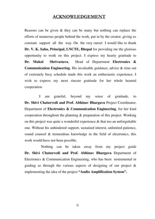
Fig 2.1 Block Diagram of Working
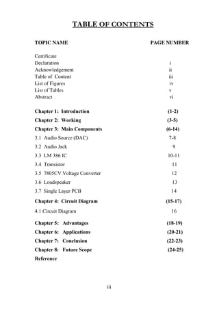
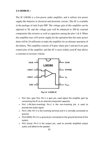
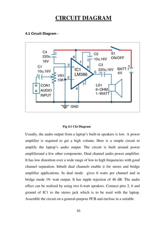
Circuit diagram of the LM386 based audio amplifier. It is built around
popular amplifier LM386 (IC1), an 8-ohm, one-watt speaker (LS1), four
capacitors and a few other components. A 6V battery is used to power this
project. Four electrolytic capacitors [two 10µF, 16V (C1 and C2) and two
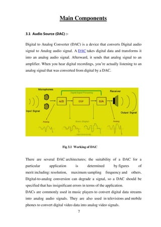
220µF, 16V (C3 and C4)] are used in this circuit. C1 is connected to the
middle terminal of 10k potentiometer VR1. C2 is connected to pins 1 and 8
of IC1. Pin 5 of IC1 is its output terminal, which is connected to speaker
LS1 through C3. C4 is connected to the positive terminal of 6V battery and
ground. Positive side of 6V is connected to pin 6 of IC1 and the other side
to ground terminal.
4](https://image.slidesharecdn.com/audioamplificationgenerator-200429112233/85/Audio-amplification-System-12-320.jpg)


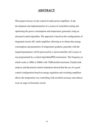
![cabinet. The circuit works off regulated 12V power supply. It is
recommended to use audio input socket in the circuit board. Use a proper
heat-sink . By varying the voltage applied or tone/volume control in Laptop,
the volume of the amplifier can be varied.
A single-side PCB for LM386 amplifier is shown in Fig. 3 and its
component layout in Fig. 4. After assembling the circuit on a PCB, enclose
it in a suitable box. Fix connector CON1 on the front panel for input and
loudspeaker LS1 at the rear side of the box. Connect VR1 on the front panel
for controlling the volume. Inverting pin 2 of IC1 is connected to ground
and non-inverting pin 3 is connected to the input terminal through VR1.
Audio input is fed to CON1. VR1 is used to control volume.
Construction and testing. Circuit diagram of the LM386 based audio
amplifier is shown in Fig. 2. It is built around popular amplifier LM386
(IC1), an 8-ohm, one-watt speaker (LS1), four capacitors and a few other
components. A 6V battery is used to power this project. Four electrolytic
capacitors [two 10µF, 16V (C1 and C2) and two 220µF, 16V (C3 and C4)]
are used in this circuit. C1 is connected to the middle terminal of 10k
potmeter VR1. C2 is connected to pins 1 and 8 of IC1. Pin 5 of IC1 is its
output terminal, which is connected to speaker LS1 through C3. C4 is
connected to the positive terminal of 6V battery and ground. Positive side of
6V is connected to pin 6 of IC1 and the other side to ground terminal to pin
4. Inverting pin 2 of IC1 is connected to ground and non-inverting pin 3 is
connected to the input terminal through VR1. Audio input is fed to CON1
VR1 is used to control volume.
17](https://image.slidesharecdn.com/audioamplificationgenerator-200429112233/85/Audio-amplification-System-25-320.jpg)


The document presents a workshop report on the 'Audio Amplification System' completed by students of Lakshmi Narain College of Technology, fulfilling the requirements for a Bachelor of Engineering degree. It outlines the project’s objectives, methodology, components, circuit diagram, and theoretical applications in audio power amplification while ensuring good power management and thermal control. Acknowledgments are made to faculty members for their guidance and support throughout the project.


