04/22/2025 1
VENUS INTERNATIONAL
COLLEGEOF TECHNOLOGY
PREPARED BY:
DISHA D. PATEL
ENROLMENT NO: 150810705004
BRANCH: COMMUNICATION SYSTEM ENGINEERING
SUBJECT: CMOS CIRCUIT DESIGN-1(2720511)
GUIDED BY:BHARGAV SIR
PROF. ANIRUDDH AMIN
HOD OF EC DEPT.
CMOS
2.
04/22/2025 CMOS 2
CONTENTS
•INTRODUCTION
• ADDER MEANS
• TYPES OF ADDERS
HALF ADDER
FULL ADDER
RIPPLE CARRY ADDER
LOOK AHEAD CARRY ADDER
CARRY-SAVE ADDERS
3.
04/22/2025 CMOS 3
INTRODUCTION
•Digital computers perform various arithmetic
operation Basic arithmetic operation is addition of two
binary digits. The first three operations produce a sum
whose length is one digit but when the last operation is
performed sum is two digits. The higher bit is called
carry. And lower bit is called sum. This operation is
called half adder. The circuit which performs addition
of three bits is a full adder.
4.
04/22/2025 CMOS 4
ADDERMEANS???
• An adder is a digital circuit that performs addition of
numbers.
• In processor it is used to calculate addresses, table indices,
and similar operations.
• It can be constructed for many numerical representations,
such as binary-coded decimal or excess-3,the most common
adders operate on binary numbers.
04/22/2025 CMOS 6
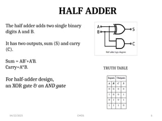
HALFADDER
The half adder adds two single binary
digits A and B.
It has two outputs, sum (S) and carry
(C).
Sum = AB’+A’B.
Carry=A*B.
For half-adder design,
an XOR gate & an AND gate
TRUTH TABLE
7.
04/22/2025 CMOS 7
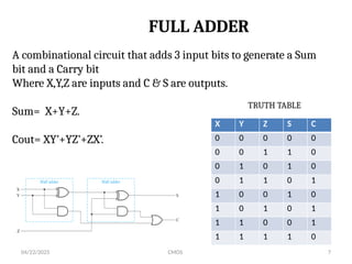
FULLADDER
A combinational circuit that adds 3 input bits to generate a Sum
bit and a Carry bit
Where X,Y,Z are inputs and C & S are outputs.
Sum= X+Y+Z.
Cout= XY’+YZ’+ZX’.
TRUTH TABLE
X Y Z S C
0 0 0 0 0
0 0 1 1 0
0 1 0 1 0
0 1 1 0 1
1 0 0 1 0
1 0 1 0 1
1 1 0 0 1
1 1 1 1 0
8.
04/22/2025 CMOS 8
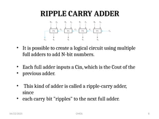
RIPPLECARRY ADDER
• It is possible to create a logical circuit using multiple
full adders to add N-bit numbers.
• Each full adder inputs a Cin, which is the Cout of the
• previous adder.
• This kind of adder is called a ripple-carry adder,
since
• each carry bit "ripples" to the next full adder.
9.
04/22/2025 CMOS 9
LOOKAHEAD CARRY UNIT
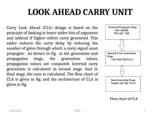
Carry Look Ahead (CLA) design is based on the
principle of looking at lower adder bits of argument
and addend if higher orders carry generated. This
adder reduces the carry delay by reducing the
number of gates through which a carry signal must
propagate . As shown in fig. in the generation and
propagation stage, the generation values,
propagation values are computed. Internal carry
generation is calculated in second stage. And in
final stage, the sum is calculated. The flow chart of
CLA is given in fig. and the architecture of CLA is
given in fig.
Flow chart of CLA
10.
04/22/2025 CMOS 10
CARRYSAVE ADDER
• In Carry Save Adder (CSA), three bits are added parallelly at
• a time. In this scheme, the carry is not propagated through the
• stages. Instead, carry is stored in present stage, and updated as
• addend value in the next stage [2]. Hence, the delay due to the
• carry is reduced in this scheme.
Block Diagram of CSA
![04/22/2025 CMOS 10
CARRY SAVE ADDER
• In Carry Save Adder (CSA), three bits are added parallelly at
• a time. In this scheme, the carry is not propagated through the
• stages. Instead, carry is stored in present stage, and updated as
• addend value in the next stage [2]. Hence, the delay due to the
• carry is reduced in this scheme.
Block Diagram of CSA](https://image.slidesharecdn.com/adders-250422175923-2f71c917/85/Adders-in-VlSI-DESIGN-electronics-pptx-10-320.jpg)