A 3-10 GHz SiGe LNA for Ultrawideband ApplicationsRFIC-IUMA
This document summarizes the design of a wideband low-noise amplifier (LNA) using SiGe transistors and on-chip inductors. The LNA was implemented in a 0.35 μm process and achieved a gain of up to 12 dB across a 3-10 GHz bandwidth. Reactive matching extended the bandwidth using LC-ladder filters. Octagonal inductors were integrated using the top metal layer. Measurements show the LNA provides up to 11.6 dB of gain with a noise figure between 3.5-7.5 dB from 2-8.5 GHz while drawing 5.3 mA from a 3.3V supply. Design guidelines are presented to optimize amplifier gain for ultrawideband
IOSR journal of VLSI and Signal Processing (IOSRJVSP) is an open access journal that publishes articles which contribute new results in all areas of VLSI Design & Signal Processing. The goal of this journal is to bring together researchers and practitioners from academia and industry to focus on advanced VLSI Design & Signal Processing concepts and establishing new collaborations in these areas.
This document describes the design of a low noise amplifier (LNA) for wireless applications operating at 900 MHz. The LNA was implemented using a 0.13um RF CMOS technology and a cascode topology with inductive source degeneration. Simulation results showed the LNA has a gain of 26 dB, noise figure of 1.04 dB, input return loss of -14 dB, output return loss of -6.55 dB, reverse isolation of -39.76 dB, and power consumption of 115uW from a 2.5V supply. The LNA meets the requirements of low noise figure, high gain and low power consumption for a 900 MHz wireless application.
A Multiband Lna with Switched Loads and Wideband Input Impedance MatchingRFIC-IUMA
This document presents a multiband low noise amplifier (LNA) topology that combines wideband input impedance matching with two switched resonant circuits in the amplifier's load. Simulations show the LNA achieves gains of 16dB and 12dB at 1.8GHz and 2.4GHz respectively, with noise figures of 2.5dB and 3.4dB. The input IP3 is 1.5dBm at 1.5GHz. The LNA was implemented in a 0.35um BiCMOS process and measures 0.771mm x 0.848mm with a power consumption of 16mW at 3.3V.
This document summarizes a 175μW 100MHz-2GHz inductorless receiver front-end in 65nm CMOS. It achieves over 17dB of gain from 100MHz to 2000MHz while consuming only 175μW from a 0.9V supply. The noise figure is 11dB and third-order intercept point is -16.8dBm. It uses a completely inductorless topology with a real input impedance of 300Ω achieved through current feedback in two stages, with a common gate stage at the input and common drain stage providing feedback current. The active area is just 0.017mm2, excluding pads.
Design and Implementation of a Low Noise Amplifier for Ultra Wideband Applica...IOSRJVSP
This paper represents the design and implementation of Low Noise Amplifier for Ultra wideband application using 0.18μm CMOS Technology. The proposed two stage LNA is for a 3-5 GHz. At supply voltage of 1.8V, for the exceed limit of 50μm of width of each transistor, the power consumption is 7.22mW. Noise figure is 4.33dB, Maximum power gain i.e. S21 is 20.4dB, S12 < -20dB, S11 < -8dB, S22 < -10dB. For the required bandwidth range, LNA is unconditionally stable and have good linearity
1) The document proposes a DC-invariant gain control technique for CMOS variable-gain low-noise amplifiers (VG-LNAs). This technique provides constant DC bias current even when the RF power gain is tuned over the gain control range.
2) A differential cascoded amplifier topology is used for the VG-LNA circuit. A gain control circuit composed of MOS transistors is connected across the differential nodes to control gain while maintaining constant bias current.
3) A 0.18 μm CMOS VG-LNA implemented with this technique showed a constant 7.8±0.5 mA current from 1.5 V supply when tuning gain from 0 to 12.3 dB at 3
IJERA (International journal of Engineering Research and Applications) is International online, ... peer reviewed journal. For more detail or submit your article, please visit www.ijera.com
This document describes the design of a 5-band graphic equalizer circuit. It uses low-cost operational amplifiers to divide the audio spectrum into 5 frequency bands, each with an independent gain control. The circuit implements a multiple feedback bandpass filter topology for each band, with component values calculated using formulas provided. Proper component selection and power supply regulation are emphasized for noise reduction and stable performance.
Design and Simulation of Low Noise Amplifiers at 180nm and 90nm TechnologiesIJERA Editor
This document describes the design and simulation of low noise amplifiers (LNAs) at 180nm and 90nm technologies. The author presents the design methodology and calculations for component values. Simulations show the LNA at 180nm has a peak frequency of 1.04502GHz and noise figure of 259.722mdB, while the 90nm LNA peaks at 1.157GHz with a noise figure of 183.21mdB. Overall, the 90nm technology performs better with a lower noise figure. The author concludes smaller feature sizes allow for lower noise performance but further optimization is still possible.
This document discusses duobinary signaling and modified duobinary signaling. Duobinary signaling is a form of partial response signaling where the pulse response spans two signaling intervals. Modified duobinary signaling corrects the deficiency of duobinary signaling having a nonzero frequency response at the origin by using a class IV partial response. It achieves a spectral shape with a gradual cutoff but requires a larger SNR to achieve the same error probability compared to binary signaling.
A CMOS Low Voltage Folded Cascode LNA for Wideband ApplicationsRFIC-IUMA
This document presents a CMOS low voltage folded cascode low noise amplifier (LNA) designed for wideband applications. Two LNAs were designed using a 0.18 μm CMOS process, a conventional cascode and the proposed folded cascode topology. Simulation results showed the folded cascode LNA achieved similar performance to the conventional cascode LNA but operated at a lower voltage of 1.8V instead of 3.6V. The low-voltage folded cascode LNA efficiently implemented wideband performance through impedance matching and a shunt peaking load.
Equal Split Wilkinson Power Divider - Project PresentationBhanwar Singh Meena
This document discusses power dividers and describes the design of an equal-split Wilkinson power divider. It explains that a power divider splits an input power signal into two or more output signals of lower power. A Wilkinson power divider uses quarter wave transformers to split power in a 3dB ratio. The document then provides specifications for designing a Wilkinson power divider to operate at 2.4GHz using a substrate with permittivity of 3.38 and thickness of 1.524mm. It calculates the impedance values needed for the divider and uses a circuit design tool to calculate the microstrip line lengths and widths.
The VM-51 is a high-performance distribution amplifier that takes one composite or SDI video input signal and distributes it to five identical outputs. It provides correct buffering and isolation between the input and outputs. It has level and equalization controls, distributes signals up to 420MHz bandwidth, and is compact in size to fit in the Kramer TOOLS family of solutions.
This document discusses research related to ultra wideband (UWB) technology. It describes designing architectures and building blocks for UWB standards, including investigating low-cost transmitter and receiver designs with a focus on localization in multipath environments. It also discusses the design of UWB radio frequency front ends and analog-to-digital converters, including prototypes that have been implemented. Finally, it mentions U-SPOT, a UWB system-level simulator for positioning and tracking applications that models wireless channels and allows analysis of localization methods and system parameters.
IJERA (International journal of Engineering Research and Applications) is International online, ... peer reviewed journal. For more detail or submit your article, please visit www.ijera.com
Design of a Low Noise Amplifier using 0.18μm CMOS technologytheijes
The International Journal of Engineering & Science is aimed at providing a platform for researchers, engineers, scientists, or educators to publish their original research results, to exchange new ideas, to disseminate information in innovative designs, engineering experiences and technological skills. It is also the Journal's objective to promote engineering and technology education. All papers submitted to the Journal will be blind peer-reviewed. Only original articles will be published.
The GT-Sat LNB series provides high quality LNBs for both linear and circular polarization reception. They were tested and found to have noise figures that matched the manufacturer's specifications, as well as strong reception on weaker signals. The series includes single, twin, quattro and quad LNB options. Circular polarization models like the GT-QDCIR40 significantly outperformed linear LNBs for receiving circular signals. Overall, the GT-Sat LNB series offers reliable reception with different options to suit various applications.
Integrated pn varactors and their application in wide ranger VCOsRFIC-IUMA
This paper presents a novel integrated p-n varactor and its application in two wide range voltage controlled oscillators (VCOs). Eleven varactors were fabricated using a 0.35 μm BiCMOS process and measured to develop a parametric model. Using this model, two VCOs were designed - VCO1 oscillates from 2.55 GHz to 5.5 GHz with a tuning range of 73.29% and phase noise of -108.56 dBc/Hz at 1 MHz offset. VCO2 oscillates from 1.087 GHz to 2.032 GHz with a tuning range of 60.6% and phase noise of -123.53 dBc/Hz at 1 MHz offset, demonstrating
The document describes the design of a low noise amplifier (LNA) circuit for a wireless local area network (WLAN) operating at 2.4 GHz. Key goals of the design are to improve noise figure and gain performance. A single-stage LNA circuit is proposed using an NMOS transistor with inductive source degeneration. Simulation results show the designed LNA achieves a forward gain of 18.8-19.2 dB and a noise figure of 1.986 dB, with over 28 dB of reverse isolation at 2.4 GHz. The document discusses various design considerations for the LNA including gain, nonlinearity, matching, noise, output voltage swing, and stability.
This document describes the design of an equal split Wilkinson power divider with the following specifications: frequency of 2.4 GHz, source and load impedances of 50 ohms, substrate permittivity of 3.38, substrate thickness of 1.524 mm, and conductor thickness of 0.15 mm. It provides background on Wilkinson power dividers, describes the calculation of microstrip line widths and lengths, shows the simulated circuit schematic and layout, and plots the resulting S-parameters which achieve the desired 3 dB power split with good port matching and isolation as expected.
This document describes a circuit design that can generate variable frequency and duty cycle output signals. It uses a crystal oscillator followed by counters and multiplexers to select different divisions of the oscillator frequency. The frequency and duty cycle can be independently controlled. Test results showed the circuit can clearly produce telephone speech through a small speaker.
The ASW610XP is a powerful closed-box subwoofer for larger rooms. It has twin 200W amplifiers and a 250mm dual voice coil driver to deliver serious bass power in a compact cabinet. The driver uses a stiff paper, Kevlar, and resin composite diaphragm to withstand the forces inside and provide slamming bass and effects without distortion.
This document provides instructions for modifying an existing large satellite dish to receive both C-band and Ku-band signals using inexpensive materials. It describes how to take an empty vegetable can, drill holes in it, and insert a copper tube to act as a combined feed for a C-band LNB on one end and Ku-band LNB on the other. With some adjustment of the positions of the LNBs and makeshift feed, both frequency ranges from a satellite can be received using this setup with only a small reduction in signal strength compared to separate feeds.
The ME 64 is a cardioid microphone head designed to be used with the K6 and K6P powering modules. It has a wide frequency response of 40-20,000 Hz and a sensitivity of 31 mV/Pa at 1 kHz. The microphone head has a nominal impedance of 200 ohms when used with the K6 module. It is suitable for applications such as reporting, interviews, dubbing, live sound reinforcement and recording with its cardioid pickup pattern and effective rejection of rear noise and feedback.
This document provides specifications for the CM Series ASW 10CM active subwoofer system. It features a 10-inch paper/Kevlar driver powered by a 500W class D amplifier. The subwoofer has adjustable low-pass filters and bass roll-off settings. Additional features include line-level and speaker-level inputs, a 12V trigger, and phase control. It measures 325mm x 325mm x 362mm and weighs 43 pounds. Finishes include gloss black, wengé, and rosenut wood veneers.
A 3-10 GHz Ultrawideband SiGe LNA with Wideband LC Matching NetworkRFIC-IUMA
Publicated in The International Society for Optical Engineering’s –
Microtechnologies for the New Millennium Design
(VLSI Circuits and Systems Conference),
Gran Canaria, España, 2007
The Approach on Influence of Biasing Circuit in Wideband Low Noise Amplifier ...IJEACS
This proposed work investigates the effects of biasing
circuit in the ultra-wideband microwave low noise amplifier
which operates between 3GHz to 10GHz. The complete circuit is
visualized the importance of every component in the design with
respect to linear measurements like Gain, Noise Figure, Return
loss under unconditionally stable condition. The design and
realization are made by using Hybrid Microwave integrated
circuit in AWR microwave office. The thing that is absolutely
necessary and frequently the difficult step in the design of an
LNA is 'biasing circuit design'. The difficulty situation arises
because traditional methods LNA by using S-parameters data
files in EDA tools provides almost all linear measurements.
Hence a number of time consuming iterations of different biasing
circuits with optimization methods may be required to reach
targeted specifications with the fixed operating point at the
desired points in the load line. Considering this behavior, various
alternate biasing circuit schemes are prepared and founded the
results associated with it. Furthermore, this paper unmistakably
clarifies the impacts of the biasing circuit by utilizing
intermodulation and harmonics distortion technique for
portrayal characterization. Different cases and sorts of the
biasing circuits with various biasing focuses have been tested and given clear perspective of the biasing ideas.
DESIGN AND ANALYSIS OF 2 GHz 130nm CMOS CASCODE LOW NOISE AMPLIFIER WITH INTE...csijjournal
This work, illustrates the development of 2 GHz Low Noise Amplifier (LNA) interfaced with square truncated edge-fed right circularly polarized patch antenna. The LNA is simulated on Agilent ADS platform with TSMC 130nm RF CMOS process. The development of cascode amplifier and its optimization has been further exemplified. The developed LNA is tuned for 2 GHz and the performance is tuned for high stability factor of 4, Gain of 19 dB which is essential for any mobile device, Noise Figure (NF) of 1.15 dB with a P1dB point at -9 dBm. Further a truncated patch antenna with right circular polarization has been simulated on EMpro. The antenna has a gain of 6.1 dB in the azimuth plane. The simulated system can be further integrated to form the RF front end of TDD2000 LTE standard mobile device.
A SiGe Front-End for a portable DVB-H ReceiverRFIC-IUMA
This paper describes the design of a low-noise amplifier (LNA) and mixer for the front-end of a portable DVB-H receiver. The LNA has a gain of 13 dB and a noise figure of 2.6 dB. The mixer has a conversion gain of 18 dB and an input referred third-order intermodulation intercept point of 16 dBm. Both the LNA and mixer were implemented in a 0.35mm BiCMOS process and together draw 5.15 mA from a 3.3V supply. Measurement results show the LNA and mixer combination provides suitable performance for a DVB-H receiver in terms of linearity and noise figure while maintaining low power consumption.
A novel cmos model design for 2 6 g hz wideband lna input matching using resi...IAEME Publication
This document describes a novel CMOS model design for a 2-6 GHz wideband low noise amplifier (LNA) input matching using resistive feedback topology for WiMAX applications. The proposed LNA uses a two-stage resistive shunt feedback structure with a simplified band pass filter to provide wide input impedance matching over 2-6 GHz. Simulation results show the LNA achieves a maximum gain of 16.5 dB, minimum noise figure of 4.2 dB, and input return loss of -12 dB across the band. The power consumption is 15 mW. A performance comparison with other published LNA designs demonstrates that this LNA is suitable for wideband applications like WiMAX.
OPTIMIZATION OF CMOS 0.18 M LOW NOISE AMPLIFIER USING NSGA-II FOR UWBVLSICS Design
A design and optimization of 3-5 GHz single ended Radio Frequency (RF) Low Noise Amplifier (LNA) for ultra-wide-band (UWB) applications using standard UMC 0.18 µm CMOS technology is reported. Designing of RF circuit components is a challenging job, since even after performing lengthy calculations and finding parameter values it is less guarantee that the design performs as expected. In view of this the optimization tool; Elitist Non-Dominated Sorting Genetic Algorithm (NSGA-II); has been employed to get the optimized starting values of components in the proposed LNA design. The obtained NSGA-II parameters were simulated using Cadence Spectre- RF simulator. The designed Low Noise Amplifier achieves a power gain of 22 dB and a minimum Noise Figure of 3 dB is achieved. It dissipates 12.5 mW of power out of 1.8 V supply
Design and Implementation of LNA at 900MHz for GSM applicationsAbdus Sami
This document summarizes the design, simulation, and implementation of a low noise amplifier (LNA) operating at 900MHz for GSM applications. The LNA was designed to have a gain of over 10dB and noise figure of less than 4dB over a 300MHz bandwidth. Simulation results showed a gain of 12dB at the center frequency with variation of ±1.3dB across the bandwidth. The noise figure was 3.9dB. The LNA achieved very high linearity and unconditional stability. The report describes the circuit design, matching network, stability considerations, and hardware implementation through layout generation and component selection.
Optimization of Cmos 0.18 µM Low Noise Amplifier Using Nsga-Ii for UWB Applic...VLSICS Design
A design and optimization of 3-5 GHz single ended Radio Frequency (RF) Low Noise Amplifier (LNA) for
ultra-wide-band (UWB) applications using standard UMC 0.18 μm CMOS technology is reported.
Designing of RF circuit components is a challenging job, since even after performing lengthy calculations
and finding parameter values it is less guarantee that the design performs as expected. In view of this the
optimization tool; Elitist Non-Dominated Sorting Genetic Algorithm (NSGA-II); has been employed to get
the optimized starting values of components in the proposed LNA design. The obtained NSGA-II
parameters were simulated using Cadence Spectre- RF simulator. The designed Low Noise Amplifier
achieves a power gain of 22 dB and a minimum Noise Figure of 3 dB is achieved. It dissipates 12.5 mW of
power out of 1.8 V supply.
This document discusses the design and simulation of low noise amplifier (LNA) circuits with different matching circuit combinations at the input and output sides. It compares the performance of LNA circuits using 'T' and 'L' type matching networks. The circuits are simulated using Advanced Design System (ADS) software. Simulation results show that the T-L matching configuration provides better gain and noise figure than L-L, L-T, and T-T matching under stability conditions. Specifically, the T-L matching achieved a forward gain of 14.14 dB and noise figure of 1.81 dB, outperforming the other matching configurations. Stabilization circuits are also applied and analyzed.
A Wide Band Low-Power Variable Gain Lna for Multi-Standard ApplicationsRFIC-IUMA
This document presents a wide-band variable gain low noise amplifier (VG-LNA) designed for multi-standard applications. The gain of the VG-LNA is controlled by adjusting the gate-to-source voltage of a cascode transistor using a peak detector and comparator. The circuit was designed in a 90nm CMOS process and consumes 10mW from a 1.5V supply. It provides a variable gain from 0-14.7dB and a noise figure of 3.2dB for high gain and 1.85dBm IIP3. The bandwidth is 300MHz to 3.73GHz. Measurement results show it meets requirements for DVB-T/H/SH digital TV systems.
Design of 10 to 12 GHz Low Noise Amplifier for Ultrawideband (UWB) SystemIJECEIAES
Balanced amplifier is the structure proposed in this article, it provides better performance. In fact, the single amplifier meets the specification for noise figure and gain but fails to meet the return loss specification due to the large mis-matches on the input & outputs. To overcome this problem one solution is to use balanced amplifier topography. In this paper, a wide-band and highgain microwave balanced amplifier constituted with branch line coupler circuit is proposed. The amplifier is unconditionally stable in the band [9-13] GHz where the gain is about 20dB. The input reflection (S11) and output return loss (S22) at 11 GHz are -33.4dB and -33.5dB respectively.
Ultra-low power 0.45 mW 2.4 GHz CMOS low noise amplifier for wireless sensor ...journalBEEI
This paper describes the design topology of a ultra-low power low noise amplifier (LNA) for wireless sensor network (WSN) application. The proposed design of ultra-low power 2.4 GHz CMOS LNA is implemented using 0.13-μm Silterra technology. The LNA benefits of low power from forward body bias technique for first and second stages. Two stages are implemented in order to enhance the gain while obtaining low power consumption for overall circuit. The simulation results show that the total power consumed is only 0.45 mW at low supply voltage of 0.55 V. The power consumption is decreased about 36% as compared with the previous work. A gain of 15.1 dB, noise figure (NF) of 5.9 dB and input third order intercept point (IIP3) of -2 dBm are achieved. The input return loss (S11) and the output return loss (S22) is -17.6 dB and -12.3 dB, respectively. Meanwhile, the calculated figure of merit (FOM) is 7.19 mW-1.
This document describes the design and simulation of a 10 GHz low noise amplifier (LNA) using GaAs high electron mobility transistors (HEMTs). Three LNA designs are presented using different approaches for the matching and biasing networks: lumped elements, distributed elements, and radial stub elements. The best performing design uses distributed elements for matching and radial stubs for biasing. The simulation shows this LNA achieves a forward gain of 14.77 dB and noise figure of 0.775 dB at 10 GHz, demonstrating better performance than prior works. Input and output return losses were also improved compared to previous LNA designs at this frequency.
The document provides information about a project guide on an ultra-wideband (UWB) antenna with electromagnetic band gap (EBG) structures. It discusses UWB technology and its features. It then describes EBG structures and their use as filters. The proposed antenna design is presented, which uses a right-angled EBG structure to provide dual band-notched capabilities at WiMAX and WLAN bands, while covering the 3-12.24 GHz UWB band. Simulation and measurement results are presented, showing the antenna meets design requirements with omni-directional radiation patterns and good return loss and voltage standing wave ratio performance.
Double feedback technique for reduction of Noise LNA with gain enhancementijceronline
In this paper we present a balun low noise amplifier (LNA) in which the gain is boosted by using a double feedback structure. The circuit is based on a conventional balun LNA with noise and distortion cancelation. The LNA is based on the combination of a common-gate (CG) stage and common-source (CS) stage. We propose to replace the load resistors by active loads, which can be used to implement local feedback loops (in the CG and CS stages). This will boost the gain and reduce the noise figure (NF). Simulation results, with a 130nm CMOS technology, show that the gain is 24dB and the NF is less than 2.7dB. The total power dissipation is only 5.4mW (since no extra blocks are required), leading to a figure-of-merit (FOM) of 3.8mW-1 using a nominal 1.2V supply. Measurement results are presented for the proposed DFBLNA included in a receiver frontend for biomedical applications (ISM and WMTS).
Low Power Consumption Mixer Based on CurrentRFIC-IUMA
This document presents a low power mixer design based on a current conveyor for wireless systems. The mixer was implemented in a 0.35 μm CMOS process and draws 580 μA from a ±1.65V supply. It achieves a total gain of 23.2 dB, a noise figure of 31.26 dB, and an IIP3 of 0 dBm. Measurement results matched simulations. The low power consumption makes the mixer suitable for wireless standards like DVB-H, WiFi, and Bluetooth.
This document summarizes the design and testing of a 2.4 GHz microstrip patch antenna with a single slot for wireless local area network (WLAN) applications. The antenna was designed to improve the bandwidth and performance of conventional microstrip patch antennas. Simulation results showed a return loss of -37.5 dB and an impedance bandwidth of 2.3-2.6 GHz. Experimental testing agreed with simulations. The antenna achieved a gain of 5 dB and has applications in mobile communications, satellite communications, and wireless personal area networks due to its compact size, broadband capability, and high gain.
10.7mW, 2.1 sq mm, 0.13um CMOS GPS radioDavid Tester
This document summarizes a fully integrated GPS radio realized in a 0.13μm CMOS technology. The radio achieves the lowest reported power consumption of 10.7mW and smallest die area of 2.1mm2. Key features include an LNA, mixer, frequency synthesizer, configurable filters, gain stages, and ADC. It operates at 1.5GHz and provides 84dB of gain. The radio represents the current state-of-the-art for low power, small area GPS receivers suitable for consumer electronics applications such as cameras and phones.
International Journal of Engineering and Science Invention (IJESI)inventionjournals
International Journal of Engineering and Science Invention (IJESI) is an international journal intended for professionals and researchers in all fields of computer science and electronics. IJESI publishes research articles and reviews within the whole field Engineering Science and Technology, new teaching methods, assessment, validation and the impact of new technologies and it will continue to provide information on the latest trends and developments in this ever-expanding subject. The publications of papers are selected through double peer reviewed to ensure originality, relevance, and readability. The articles published in our journal can be accessed online
Similar to A Feedback Wideband lna for UWB Applications (20)
Presentación del Trabajo Fin de Grado de Guillermo Ojeda, titulado Diseño de un Amplificador Integrado en configuración Doherty en tecnología GaN. Defendido el mes de julio de 2017 con mención en matrícula de honor.
Presentación del Trabajo Fin de Grado de Guillermo Ojeda, titulado Diseño de un Cabezal de Recepción para el estándar IEEE 802.15.4 en tecnología CMOS de 65 nm. Defendido el mes de julio de 2017 con mención en matrícula de honor.
Diseño de un Amplificador de Ganancia Programable para un Receptor IEEE 802.1...RFIC-IUMA
Este documento describe el diseño de un amplificador de ganancia programable para un receptor IEEE 802.15.4 usando tecnología CMOS 0.18 μm. Se diseñó un amplificador operacional, una resistencia variable y un varactor para cumplir con especificaciones de bajo consumo, alta linealidad y ancho de banda constante. Se simuló el amplificador, el receptor completo y se compararon los resultados con otros diseños, mostrando un consumo de potencia menor de 6.24 mW y una ganancia de 87 dB.
Diseño de un receptor de wake-up para WSN basado en la arquitectura Uncertain-IFRFIC-IUMA
Este documento presenta el diseño a nivel de layout de los componentes clave de un receptor de "wake-up" para redes de sensores inalámbricas basado en la arquitectura "Uncertain-IF". Se describe el diseño del layout del mezclador, detector de envolvente diferencial y etapa amplificadora, así como su simulación. El objetivo es realizar el diseño a nivel de layout del esquemático obtenido en un trabajo de fin de máster previo para optimizar la sensibilidad, consumo y alcance del receptor manteniendo un b
Implementación física y verificación de un cabezal de recepción para el están...RFIC-IUMA
Este documento describe el diseño e implementación física de un cabezal de recepción para el estándar IEEE 802.15.4 en tecnología CMOS de 0.18 μm. Se presenta la arquitectura del cabezal de recepción basada en Low-IF, que incluye un amplificador de bajo ruido, un mezclador y dos amplificadores de transimpedancia. Se detalla el proceso de diseño a nivel de layout de cada bloque y del cabezal completo en Cadence. Finalmente, se muestran los resultados de simulación para
Diseño de un transmisor para el estándar IEEE 802.15.4 en tecnología CMOS 0.1...RFIC-IUMA
Este documento describe el diseño de un transmisor para el estándar IEEE 802.15.4 en tecnología CMOS 0.18 μm. Se presentan los objetivos de bajo consumo y área reducida. Se describe el diseño de un mezclador pasivo doblemente balanceado y de un amplificador de potencia de dos etapas de clase A. Finalmente, se muestran los resultados de simulación del mezclador y del amplificador de potencia.
Diseño de un filtro polifásico para un receptor IEEE 802.15.4 en tecnología...RFIC-IUMA
Este documento describe el diseño de un filtro polifásico para un receptor IEEE 802.15.4 en tecnología CMOS 0.18 μm. El objetivo principal es diseñar un filtro polifásico de bajo consumo para eliminar las frecuencias imagen en la banda de 2.4 GHz. El documento comienza explicando la teoría básica de los filtros y luego describe el diseño de un filtro paso bajo pasivo, un filtro activo basado en la topología Gm-C y la teoría de los filtros polifásicos. Finalmente
Sistema de localización de objetos basado en tecnología de Código Abierto de ...RFIC-IUMA
Este documento describe el diseño y desarrollo de un sistema de localización de objetos basado en la tecnología Arduino. El sistema utiliza una placa Arduino Uno, un módulo GPRS y un módulo GPS para determinar la ubicación de un objeto y enviar un SMS si se aleja de una ubicación de referencia. El documento explica el estudio de la tecnología Arduino, el diseño del localizador, la programación de sus funciones y las pruebas realizadas para verificar su funcionamiento.
Diseño de un circuito Wake-up para redes de sensores inalámbricasRFIC-IUMA
Este documento describe el diseño de un circuito wake-up para redes de sensores inalámbricas. Se implementó un circuito wake-up pasivo usando diodos rectificadores y un filtro RC para generar la señal de activación. También se diseñó el circuito en una PCB y se implementó un módulo digital usando un microcontrolador MSP430 y un receptor AS3933. Las mediciones mostraron que el circuito wake-up puede despertar sensores a distancias de hasta 40 metros con un consumo de solo 3 μA en modo dormido.
Caracterización del equipo de prácticas ME1000 para el diseño de circuitos de RFRFIC-IUMA
El documento describe el equipo de prácticas ME1000 y sus subsistemas. Se divide en cuatro bloques: introducción, subsistemas del equipo, transceptor RF completo y valoración del proyecto. En la introducción se describen los objetivos de formación y aplicados al equipo. Los subsistemas analizados incluyen el amplificador de potencia, amplificador de bajo ruido y otros. En el bloque de transceptor RF completo se analizan las cabeceras de RF y el modelo comportamental del sistema. El último bloque contiene las conclusiones y presupuesto.
Diseño de un cabezal de recepción para el estándar IEEE 802.15.4 en tecnologí...RFIC-IUMA
Este documento describe el diseño de un receptor de bajo consumo para el estándar IEEE 802.15.4 en la banda de 2,4 GHz utilizando la tecnología CMOS 0,18 μm. El objetivo es diseñar un cabezal de recepción basado en la arquitectura Low-IF que incluya un amplificador de bajo ruido, un mezclador y un amplificador de transimpedancia con bajo ruido y alta linealidad. Se presentan los detalles del diseño y simulación de cada bloque, así como las característic
Sistema de estabilización de cámara para cartografía aéreaRFIC-IUMA
Este documento describe el diseño de un sistema de estabilización de cámara para cartografía aérea. El sistema utiliza sensores inerciales, actuadores lineales y un microcontrolador para corregir los ángulos de cabeceo, alabeo y guiñada de una cámara durante la toma de fotografías aéreas. El documento también cubre el diseño de hardware, software y estructura necesarios para el sistema de estabilización.
Control automático de un sistema de riegoRFIC-IUMA
Este documento describe el diseño e implementación de un sistema de riego automático controlado. Se utilizarán placas Arduino, módulos XBee para comunicación inalámbrica entre nodos, y un módulo GPRS para control remoto. El sistema constará de 4 zonas de riego con sensores de humedad, iluminación, nivel de agua y batería. El controlador automatizará el riego basado en los datos de los sensores de forma autónoma y permitirá el monitoreo y control remoto a través de GPRS.
Diseño de un LNA basado en convertidores de corriente utilizando técnicas de ...RFIC-IUMA
Este documento describe el diseño de un amplificador de bajo ruido (LNA) basado en convertidores de corriente utilizando técnicas de cancelación de ruido en tecnología CMOS 65nm. Presenta los conceptos de convertidores de corriente y técnicas de cancelación de ruido, y describe el diseño a nivel de esquemático y layout de un LNA que utiliza estas técnicas para reducir la figura de ruido. Los resultados muestran que el LNA propuesto cumple con los requisitos de baja figura
Implementación de una red de sensores inalámbrica para la monitorización de e...RFIC-IUMA
Este documento presenta un proyecto final de carrera sobre el uso de redes de sensores inalámbricos para la detección de patologías constructivas. Se estudian las patologías de la construcción, el hardware libre Waspmote y sus sensores, y se realizan pruebas con los sensores y la placa Waspmote. El documento concluye evaluando la capacidad de almacenamiento de datos y modos de ahorro de batería, e indica posibles líneas futuras como pruebas en estructuras o integrar nuevos sensores y comunicaciones
Comunicaciones a través de voz sobre IP. Casos prácticos, adaptación empresar...RFIC-IUMA
Este documento presenta un resumen de un proyecto de investigación sobre la voz sobre IP (VoIP). El proyecto analiza el estado actual de las redes de nueva generación, la telefonía tradicional frente a la VoIP, los dispositivos y software necesarios para VoIP, casos prácticos de implantación de VoIP y conclusiones. El documento está estructurado en 7 capítulos que cubren la introducción, el estado de las redes, telefonía tradicional vs VoIP, dispositivos VoIP, casos prácticos, conclusiones y presupuesto.
Diseño de un receptor de “Wake up” para redes de sensores inalámbricas median...RFIC-IUMA
Este documento describe el diseño de un receptor de wake-up para redes de sensores inalámbricas utilizando una arquitectura Uncertain-IF. El objetivo es diseñar un receptor de muy bajo consumo para despertar nodos en la red de forma asíncrona. Se explican los componentes clave del receptor como el generador de la señal OOK, el mezclador y su red de adaptación. El diseño se realiza mediante simulaciones en ADS para validar el funcionamiento y optimizar el consumo.
Estudio y Análisis de un transceptor de largo alcance LORATM SX1272RFIC-IUMA
Este documento presenta un proyecto de fin de carrera sobre el estudio y análisis de un transceptor LoRa de largo alcance SX1272. Explica las técnicas FHSS y FEC, describe el transceptor SX1272 y la modulación LoRa, analiza el kit de desarrollo, presenta medidas de alcance, concluye sobre la robustez de LoRa frente al ruido y su potencial para Internet de las Cosas, y resume el presupuesto.
Sistema para monitorizar y controlar instalaciones de forma remota utilizando...RFIC-IUMA
Este documento presenta un sistema para monitorear y controlar instalaciones de forma remota utilizando software libre. El sistema consta de tres bloques: una unidad de control basada en Raspberry Pi, un servidor y base de datos, y una aplicación web. El sistema permite la monitorización en tiempo real de variables como temperatura, humedad y luminosidad, así como el control remoto de dispositivos como cámaras, LEDs y motores. El documento describe el diseño y funcionamiento de cada bloque y del sistema completo.
Implementación de una red de sensores inalámbrica para la monitorización de e...RFIC-IUMA
Este documento resume un proyecto de implementación de una red de sensores inalámbrica para la monitorización de explotaciones vitivinícolas en Canarias. El proyecto consta de tres bloques: 1) introducción y marco tecnológico, 2) componentes de la red y su implementación, y 3) software de monitorización. Se utiliza una red ZigBee formada por nodos Arduino equipados con sensores de temperatura, humedad y luz, para controlar parámetros en la producción del vino. Los datos se envían a una aplicación
ZKsync airdrop of 3.6 billion ZK tokens is scheduled by ZKsync for next week.pdfSOFTTECHHUB
The world of blockchain and decentralized technologies is about to witness a groundbreaking event. ZKsync, the pioneering Ethereum Layer 2 network, has announced the highly anticipated airdrop of its native token, ZK. This move marks a significant milestone in the protocol's journey, empowering the community to take the reins and shape the future of this revolutionary ecosystem.
Cleades Robinson, a respected leader in Philadelphia's police force, is known for his diplomatic and tactful approach, fostering a strong community rapport.
UnityNet World Environment Day Abraham Project 2024 Press ReleaseLHelferty
June 12, 2024 UnityNet International (#UNI) World Environment Day Abraham Project 2024 Press Release from Markham / Mississauga, Ontario in the, Greater Tkaronto Bioregion, Canada in the North American Great Lakes Watersheds of North America (Turtle Island).
World economy charts case study presented by a Big 4
World economy charts case
World economy charts case study presented by a Big 4
World economy charts case study presented by a Big 4World economy charts case study presented by a Big 4
World economy charts case study presented by a Big 4
World economy charts case study presented by a Big 4World economy charts case study presented by a Big 4World economy charts case study presented by a Big 4World economy charts case study presented by a Big 4World economy charts case study presented by a Big 4World economy charts case study presented by a Big 4World economy charts case study presented by a Big 4World economy charts case study presented by a Big 4World economy charts case study presented by a Big 4World economy charts case study presented by a Big 4World economy charts case study presented by a Big 4World economy charts case study presented by a Big 4World economy charts case study presented by a Big 4World economy charts case study presented by a Big 4study presented by a Big 4
Methanex is the world's largest producer and supplier of methanol. We create value through our leadership in the global production, marketing and delivery of methanol to customers. View our latest Investor Presentation for more details.
Collective Mining | Corporate Presentation - June 2024
A Feedback Wideband lna for UWB Applications
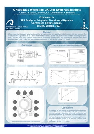
1. A Feedback Wideband LNA for UWB Applications
R. Pulido, H. García, J. del Pino, S. L. Khemchandani, A. Hernández
Dto. de Ingeniería Electrónica y Automática (DIEA) & Instituto Universitario de Microelectrónica Aplicada (IUMA). Universidad de Las Palmas de Gran Canaria (Spain)
Publicated in
XXII Design of Integrated Circuits and Systems
Conference (Internacional),
Sevilla, España, 2007
Abstract
A fully-integrated feedback wide band amplifier is implemented in a standard SiGe low cost 0.35 µm process. The
circuit provides a gain from 13 to 7 dB in the band between 3.1 to 10.6 GHz. In the same band the noise figure varies
from 3.6 to 4.7 dB in band. Design guidelines for optimizing amplifier gain and noise figure are presented. Chip
dimensions are 0.580 × 0.636 mm and power dissipation is 19 mW, drawn from a 3.3V supply.
LNA Design Measurements & Simulations
Schematic of a receiver for UWB. a) S21 with different consumption. And b ) Feedback amplifier post-layout S21 and S12.
0
a) Feedback amplifier post-layout Phase S21.b) Feedback amplifier post-layout S21 and S12.
Basic Distributed Amplifier schematic.
Post-layout, 1 dB compression point at 6 GHz.
Conclusions
In this paper we have reported the fundamental design aspects of
wideband low-noise feedback amplifiers with SiGe transistors and
on chip inductors. A description of the LNA configuration was
explained emphasizing the influence of the design parameters in
the circuit performance. The circuit was implemented in a standard
low cost 0.35 µm process and provides a worst case gain from 13
to 7 dB in the band between 3.1 to 10.6 GHz. The noise figure
ranges from 3.6 to 4.7 dB in the same band. The circuit only
Wide band amplifier layout including pads for on chip measurements. requires 5.75 mA from a 3.3-V supply.
INSTITUTO UNIVERSITARIO DE MICROELECTRÓNICA APLICADA (IUMA)
UNIVERSIDAD DE LAS PALMAS DE GRAN CANARIA (ULPGC)