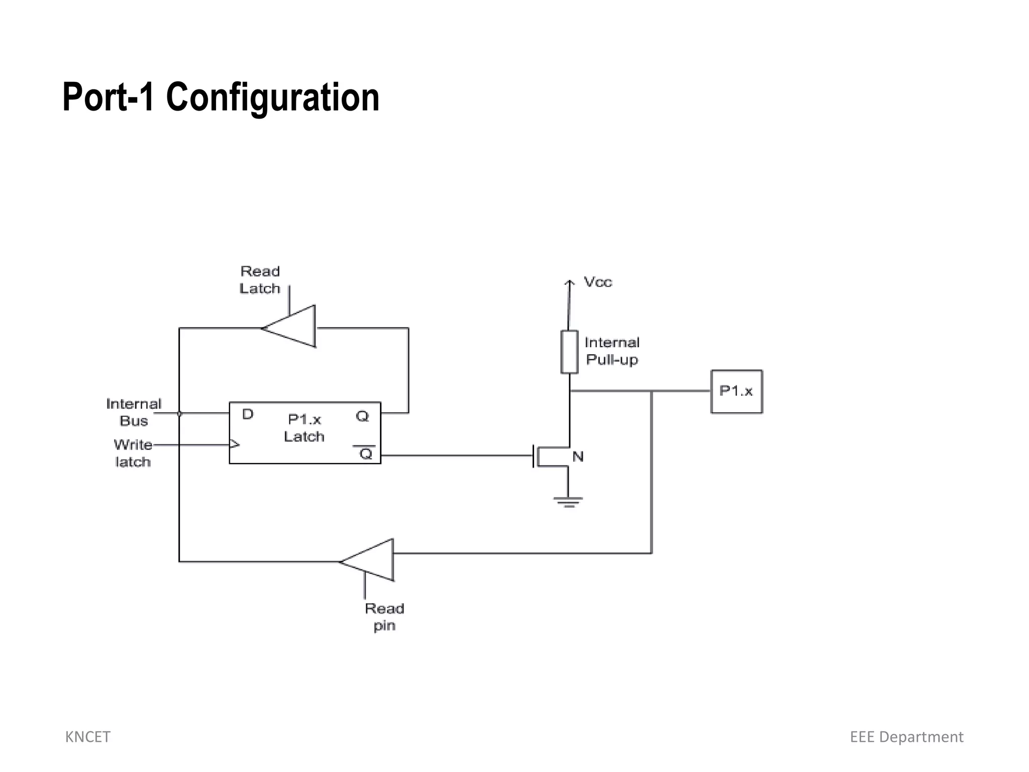
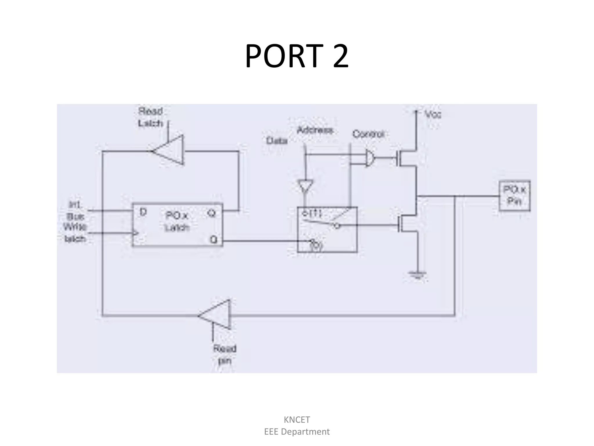
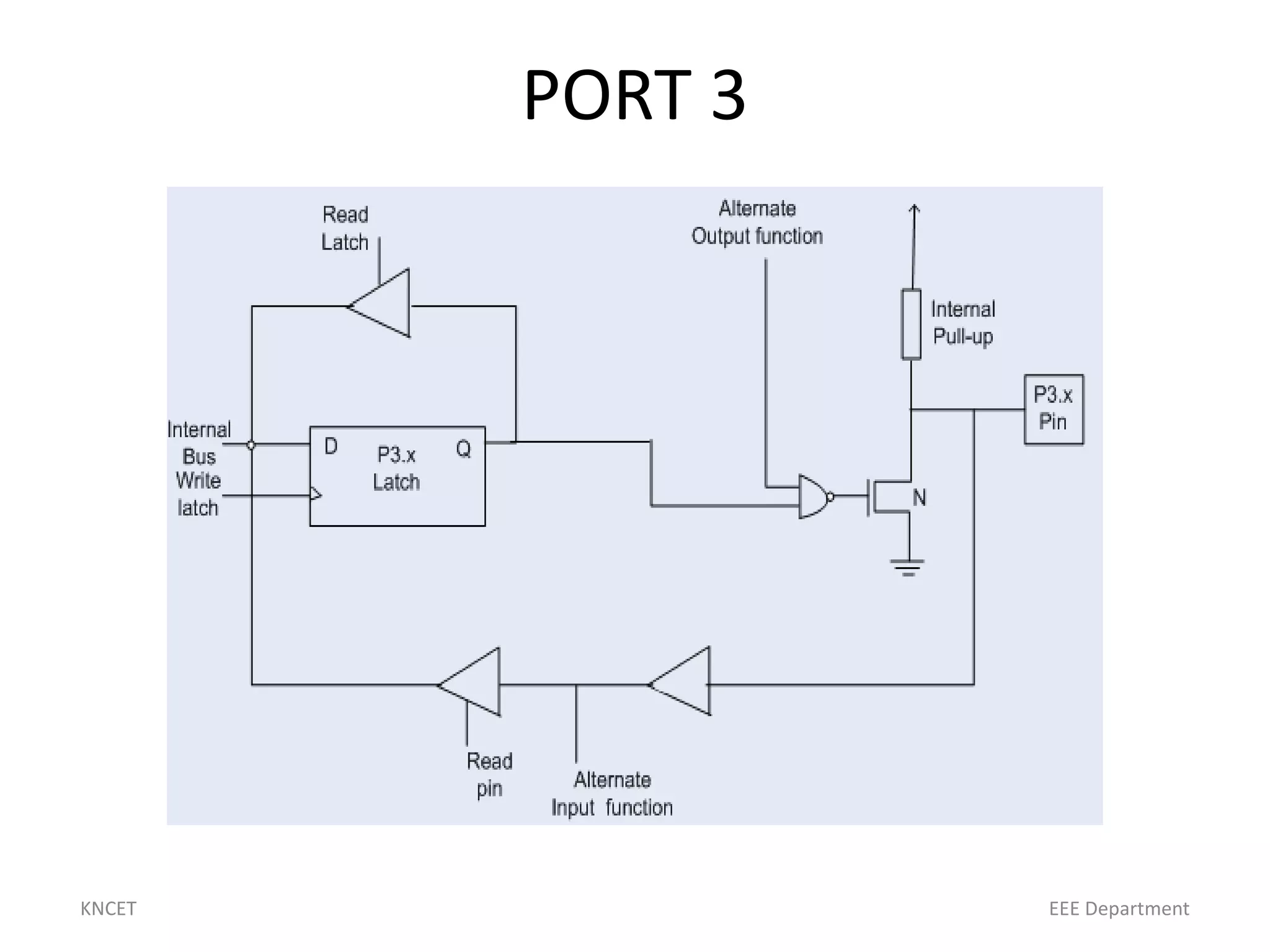
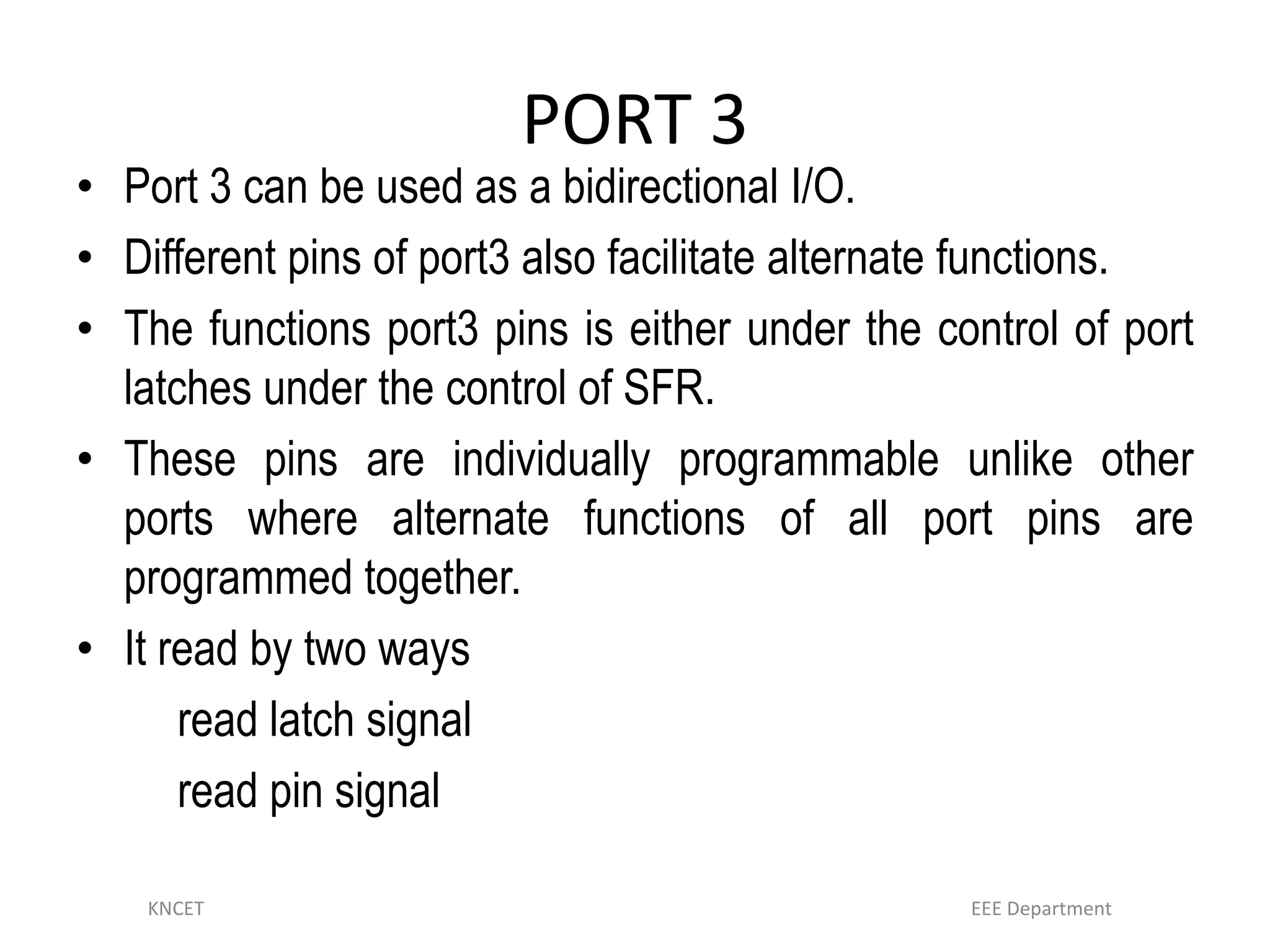
3. • Port 0 and 2 together can be used to address the external
memory. Port 0 can also be used to exchange data from
the external port. accessing 64K bytes of external memory,
it needs a path for the 16 bits of the address. P0 gives
lower Byte of Address.
KNCET EEE Department
4. PORT 1
• Port 1 is a bidirectional I/O port with internal pull ups
• The circuit has 3 FET.
• When port 1 as input port logic level is loaded
to the latch .This is will turn off the FET 1.
• This will effectively float the port pin to high impedance
state and will be connected the pin read buffer.
• The pin is at logic level 1 is at instant.
• An external device may place a 0 by driving the pin ground
or it may place a 1 on pin by leaving it at logic state.
KNCET EEE Department
5. • When used as output port the value will be loaded to the
latch.
• The latches which contain level 1 will turn off FET T1 and
will drive the pin high through pull register formed by T2
and T3.
• This will ground the pin and it will show logic level 0.
• The latches containing level 0 will turn on FET 1
KNCET EEE Department
7. PORT 2
• Port 2 can be used as a bidirectional I/O port
• It can used as a higher order internal bus for external memory
interface
• When used as a input port logic level is stored in latch
• T1 is turned of and floats in high impedance state. The pin is
directly connected pin read buffer.
• The external device can place 0 or 1.
• When used as output port the working of port is similar to port 1 that
means the latch o will turn on FET T1.
• Thus ground the pin
• The latch containing 1 will turn off T1 and pin will be driven to logic
level 1.
• When port is used to higher order address bit for external memory
access the control . They are directly connected pin trough FET
KNCET
EEE Department
9. PORT 3
• Port 3 can be used as a bidirectional I/O.
• Different pins of port3 also facilitate alternate functions.
• The functions port3 pins is either under the control of port
latches under the control of SFR.
• These pins are individually programmable unlike other
ports where alternate functions of all port pins are
programmed together.
• It read by two ways
read latch signal
read pin signal
KNCET EEE Department
10. Conclusion:
• The port configuration of 8051 microcontroller are
explained in detail manner.
KNCET
EEE Department