This document presents a new DFT-based approach for detecting and correcting gain mismatch in time-interleaved ADCs. It introduces the gain mismatch problem in TI-ADCs and how it reduces the spurious free dynamic range. The proposed method uses the discrete Fourier transform to detect the gain mismatch between ADC sub-channels based on the difference between the ideal DFT and actual DFT. It then introduces a feedback system using this difference signal to iteratively correct the gain mismatch. Simulation results show the approach improves SFDR by more than 30dB by correcting a ±2% gain mismatch in a two-channel TI-ADC.
![A New DFT based Approach for Gain Mismatch
Detection and Correction in Time-Interleaved ADCs
Yashar Hesamiafshar#1, Sanaz Momeni*2
#
School of Electrical and Computer Engineering, University of Tehran
College of Engineering (Campus No. 2), North Kargar Ave., Tehran, Iran
1
y.hesamiafshar@ece.ut.ac.ir
*
Microelectronics Research Lab
Urmia University
Abstract— This report introduces a new approach for detection
and correction of gain mismatch between ADC sub-channels in II. GAIN MISMATCH PROBLEM
time- interleaved ADCs. Based on discrete Fourier transform, Fig. 1 illustrates the architecture of a two-channel TI-ADC.
this technique uses a simple approach for gain mismatch
Ideally, both ADC sub-channels have identical gain i.e. α=0.
correction. MATLAB simulation results are represented for
correction of ±2% gain mismatch in a two-channel time-
In practice however there exists a finite gain mismatch
interleaved ADC where the proposed approach improves the between ADC sub-channels modeled by a non-zero value of α.
SFDR by more than 30dB. In order to maintain the resolution of the TI-ADC within the
resolution of each sub-channel ADC the mismatch issue must
I. INTRODUCTION be addressed. The scope of this paper is elimination of the
With increasing number of wideband signal sources the gain mismatch in a two-channel TI-ADC.
demand for high speed high resolution analog to digital
converters (ADCs) is soaring. Time-interleaved (TI) ADCs
have found to be the only solution for digitization of very high
bandwidth signals by surpassing the single ADC speed limit
[1]. However the efficacy of the TI-ADCs can easily be
compromised by the mismatch between the ADC sub-
channels. Mismatch in terms of offset, gain and timing
degrades the spurious free dynamic range (SFDR) and signal
to noise and distortion ratio (SNDR) of the whole ADC by
introducing mismatch induced harmonic distortion [2,3]. Fig. 1. Time Interleaved ADC Architecture
However the impairments incurred by mismatch in TI-ADCs
can be corrected by incorporating a calibration scheme [2-6]. Fig. 2 shows how the gain mismatch between two ADC sub-
In [2] the mismatch calibration is carried out by utilizing an channels reduces the SFDR of a 12b TI-ADC by drawing the
extra ADC or so called reference ADC with the subsequent SFDR versus different mismatch values. For example only 1%
least squares correction method. In [3] the mismatch problem of gain mismatch between ADC sub-channels reduces the
is tackled by incorporating an equalizer structure imposing SFDR of the TI-ADC to 45dB which is almost equivalent to
additional power consumption overhead by utilizing a resolution of an 8b ADC. Next section describes the proposed
complicated structure. In [4] linear and nonlinear mismatches approach for detection and correction of the gain mismatch in
are attenuated by use of specific signal sources for foreground a two-channel TI-ADC.
calibration which limits its application for special cases such
as automatic test equipments. This report addresses the gain
mismatch problem by proposing an efficient structure for gain
mismatch detection and correction. Uniqueness of this
approach is detection and correction of the gain mismatch in
an efficient way. The structure of this report is as following.
In section II the effect of gain mismatch on the SFDR of the
TI-ADC is discussed. Part III introduces the proposed method
for detection and correction of the gain mismatch. Section IV
suggests a more efficient implementation of the invented idea.
Finally, the MATLAB simulation results of the proposed
system are shown in section V.
Fig. 2. Effect of gain mismatch between ADC sub-channels on SFDR
978-1-4244-8971-8/10$26.00 c 2010 IEEE](https://image.slidesharecdn.com/36-101202234845-phpapp01/85/36-1-320.jpg)
![A New DFT based Approach for Gain Mismatch
Detection and Correction in Time-Interleaved ADCs
Yashar Hesamiafshar#1, Sanaz Momeni*2
#
School of Electrical and Computer Engineering, University of Tehran
College of Engineering (Campus No. 2), North Kargar Ave., Tehran, Iran
1
y.hesamiafshar@ece.ut.ac.ir
*
Microelectronics Research Lab
Urmia University
Abstract— This report introduces a new approach for detection
and correction of gain mismatch between ADC sub-channels in II. GAIN MISMATCH PROBLEM
time- interleaved ADCs. Based on discrete Fourier transform, Fig. 1 illustrates the architecture of a two-channel TI-ADC.
this technique uses a simple approach for gain mismatch
Ideally, both ADC sub-channels have identical gain i.e. α=0.
correction. MATLAB simulation results are represented for
correction of ±2% gain mismatch in a two-channel time-
In practice however there exists a finite gain mismatch
interleaved ADC where the proposed approach improves the between ADC sub-channels modeled by a non-zero value of α.
SFDR by more than 30dB. In order to maintain the resolution of the TI-ADC within the
resolution of each sub-channel ADC the mismatch issue must
I. INTRODUCTION be addressed. The scope of this paper is elimination of the
With increasing number of wideband signal sources the gain mismatch in a two-channel TI-ADC.
demand for high speed high resolution analog to digital
converters (ADCs) is soaring. Time-interleaved (TI) ADCs
have found to be the only solution for digitization of very high
bandwidth signals by surpassing the single ADC speed limit
[1]. However the efficacy of the TI-ADCs can easily be
compromised by the mismatch between the ADC sub-
channels. Mismatch in terms of offset, gain and timing
degrades the spurious free dynamic range (SFDR) and signal
to noise and distortion ratio (SNDR) of the whole ADC by
introducing mismatch induced harmonic distortion [2,3]. Fig. 1. Time Interleaved ADC Architecture
However the impairments incurred by mismatch in TI-ADCs
can be corrected by incorporating a calibration scheme [2-6]. Fig. 2 shows how the gain mismatch between two ADC sub-
In [2] the mismatch calibration is carried out by utilizing an channels reduces the SFDR of a 12b TI-ADC by drawing the
extra ADC or so called reference ADC with the subsequent SFDR versus different mismatch values. For example only 1%
least squares correction method. In [3] the mismatch problem of gain mismatch between ADC sub-channels reduces the
is tackled by incorporating an equalizer structure imposing SFDR of the TI-ADC to 45dB which is almost equivalent to
additional power consumption overhead by utilizing a resolution of an 8b ADC. Next section describes the proposed
complicated structure. In [4] linear and nonlinear mismatches approach for detection and correction of the gain mismatch in
are attenuated by use of specific signal sources for foreground a two-channel TI-ADC.
calibration which limits its application for special cases such
as automatic test equipments. This report addresses the gain
mismatch problem by proposing an efficient structure for gain
mismatch detection and correction. Uniqueness of this
approach is detection and correction of the gain mismatch in
an efficient way. The structure of this report is as following.
In section II the effect of gain mismatch on the SFDR of the
TI-ADC is discussed. Part III introduces the proposed method
for detection and correction of the gain mismatch. Section IV
suggests a more efficient implementation of the invented idea.
Finally, the MATLAB simulation results of the proposed
system are shown in section V.
Fig. 2. Effect of gain mismatch between ADC sub-channels on SFDR
978-1-4244-8971-8/10$26.00 c 2010 IEEE](https://image.slidesharecdn.com/36-101202234845-phpapp01/75/36-1-2048.jpg)
![III. PROPOSED DFT BASED CONCEPT FOR GAIN MISMATCH The second term in (6) is due to the gain mismatch being
CORRECTION proportional with mismatch value of α. This term is the basis
for the proposed gain error detection mechanism. The
Discrete Fourier transform (DFT) of a periodic difference between the ideal DFT and the gain mismatched
sequence, X ( e j 2π nk / N ) , is defined by the following equation: DFT is define by D1 as following (7):
N −1
X k = ∑ x [ n] e
− j 2π kn / N
(1)
D1 = Y2 e( ) − Y ( e ) = α sin π [t ]
jπ
1
jπ
T
0 (7)
n =0 Note that the sign of D1 is uncertain due to random nature of
Where the x[n] denotes the periodic sequence with period t0 . In order to determine the sign of the gain mismatch value
N. The DFT of the output sequence of TI-ADC will be the the difference D1 is further evolved to obtain D2, defined as
integral part of the proposed approach for gain mismatch following (8):
detection. For simplicity of implementation the DFT of TI- π
ADC output is carried out at Nyquist frequency where the D2 = α sin [t0 ] (8)
T
angular frequency is equivalent to π , by assuming k=1, and
The term D2 is the very signal for detecting the sign and
the resulting sequence period is N=2. In this case (1) is
magnitude of the gain mismatch. This difference when applied
reduced to (2) by:
2 −1 2−1
to an accumulator within a closed loop as shown in Fig. 3 will
X 1 = ∑ x [ n] e = ∑ x [ n](−1)n
− jπ n
(2) result in complete removal of gain mismatch due to infinite
n=0 n=0 loop gain of the proposed feedback system.
Where the only calculation required is addition and
subtraction operations with no need for multiplication. The
output sequence of the TI-ADC is defined by y[n]. For
further simplification of the system implementation, DFT of
samples of a sinusoid located at Nyquist frequency is utilized
as the basis for gain mismatch detection resulting in a
sequence with period of two. In ideal case when no mismatch
incurs between ADC sub-channels the proposed output
sequence is defined by y1 [n] as:
⎧ π π
⎪ sin T [t0 + nT ] = sin T [t0 ] n = even
⎪
y1[n] = ⎨ (3)
⎪sin π [t + nT ] = − sin π [t ] n = odd Fig. 3. Proposed system for gain mismatches detection and correction
⎪ T 0
⎩ T
0
IV. SIMPLE IMPLEMENTATION BY DECIMATION
Where T denotes the sampling period and t0 is the initial
time of the waveform. The DFT of the y1 [n] is defined as: As discussed in section II, the gain mismatch detection
2 −1
π mechanism relies on the DFT of a sinusoid located at the
( )
Y1 e = ∑ sin [t0 + nT ] e
jπ
T
− jπ n
= Nyquist frequency. This structure can efficiently be
n =0
implemented by virtue of decimation. Note that K times
⎛ π π ⎞ π decimation of a sinusoid located at frequency Fs/2K will alias
⎜ sin [t0 ] − sin [t0 + T ] ⎟ = 2sin [t0 ] (4)
⎝ T T ⎠ T it to the Nyquist frequency. This fact is utilized for modifying
Note that the proposed DFT value is equivalent to the the system of Fig. 3 into Fig. 4. The new system receives the
channel output with even index of samples (3). In practice ADC output samples at K times lower rate resulting in lower
however, gain mismatch between ADC sub-channels, defined clock frequency for the proposed systems with K times lower
by α, deviates the TI-ADC output sequence from samples of a power consumption as a consequence. Note that with
pure sinusoid (5): increasing the value of K the settling time of the coefficient
⎧ π π correction is also increasing which is quite negligible.
⎪ sin [ t0 + nT ] = sin [t0 ] n = even
⎪ T T
y2 [n] = ⎨ (5)
⎪(1 + α ) sin π [t + nT ] = − (1 + α ) sin π [t ] n = odd
⎪
⎩ T
0
T
0
where outputs of ADC sub-channels are distinguished by
even and odd sequences. DFT for y2 [n] is obtained as
following:
2 −1
⎛ π π ⎞
( )
Y2 e = ∑ y2 [ n ] e
jπ
n =0
− jπ n
= ⎜ sin [ t0 ] − (1 + α ) sin [ t0 + T ] ⎟
⎝ T T ⎠
π π
= 2 sin [t0 ] + α sin [t0 ] (6)
Fig. 4. Efficient Implementation of proposed calibration scheme
T T](https://image.slidesharecdn.com/36-101202234845-phpapp01/85/36-2-320.jpg)
![0.005
0
Correction Coefficient
Correction Coefficient
-0.005
-0.0203
-0.01
-0.0204
-0.015 -0.0205
-0.02
-0.025
0 20 40 60 80 100 120
Time (secs)
(a) (b)
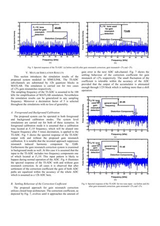
Fig. 7. Settling behaviour of the correction coefficient in the proposed system, (a) gain mismatch= +2%, (b) gain mismatch= -2%
CONCLUSION
An efficient architecture is proposed for gain mismatch frequency. The MSB of the ramp signal is taken as its
detection and correction in TI-ADCs. The uniqueness of sign bit assuming a signed representation.
the proposed approach is the low power consumption as
well as simplicity of the implementation. This approach
is verified by modeling of the gain mismatch correction REFERENCES
system in MATLAB. Simulation results show that the [1] J.William, C. Black, and D. A. Hodges, “Time interleaved converter
invented system corrects the gain mismatch within the arrays,” IEEE J. Solid-State Circuits, vol. SC-15, no. 12, pp. 1022–
1028,Dec. 1980.
required accuracy of the TI-ADC. [2] J. Balakrishnan et al “Parameter mismatch estimation in a parallel
interleaved ADC” ISCAS 2009
APPENDIX [3] J. Goodman “Polyphase Nonlinear Equalization of Time-Interleaved
Analog-to-Digital Converters” IEEE J. Selected Topics in Signal
As discussed in part III, D1 is the signal containing gain
Processing, vol. 3, no. 3, Jun. 2009
mismatch term (7) and needs to be modified into D2 (8) [4] K. Asami et al “Techniques to improve the performance of Time-
to have a signal containing both magnitude and sign of Interleaved A-D Converters with Mismatches of Non-Linearity” IEICE
the gain mismatch. For this purpose D1 is multiplied by Trans. Fundamentals, vol.E92-A, no.2, Feb 2009
[5] Cheng-Chung Hsu, Fong-Ching Huang, Chih-Yung Shih, Chen-Chih
a sign bit which is derived as shown in Fig. 8. It can be
Huang, Ying-Hsi Lin, Chao-Cheng Lee, Razavi, B., “An 11b 800MS/s
shown that only at DC as well as Nyquist frequency the Time-Interleaved ADC with Digital Background Calibration” in Proc.
accumulator output builds up resulting in a ramp signal IEEE Int. Solid-State Circuits Conf. Dig. Tech. Papers, 2007
whose sign is taken as the required sign bit. Since the San Francisco, CA, Feb. 2006, vol. 650, pp. 464–615
[6] Wei-Mei Lee, Cheng-Yeh Wang, and Jieh-Tsorng Wu, “A
input signal is assumed to have zero DC value the only
CMOS 15-bit 125-MS/s Time-Interleaved ADC With Digital
frequency component resulting in a ramp is the Nyquist Background Calibration” IEEE J. Solid-State Circuits, vol. 42,
no. 10, pp. 1900–1911, Oct. 2007.
Fig. 8. Sign bit extraction](https://image.slidesharecdn.com/36-101202234845-phpapp01/85/36-4-320.jpg)


![Digital Signal Processing[ECEG-3171]-Ch1_L06](https://cdn.slidesharecdn.com/ss_thumbnails/dspl6ch2-180427094424-thumbnail.jpg?width=640&height=640&fit=bounds)


![Digital Signal Processing[ECEG-3171]-Ch1_L05](https://cdn.slidesharecdn.com/ss_thumbnails/dspl5ch2-180427094424-thumbnail.jpg?width=640&height=640&fit=bounds)

![Digital Signal Processing[ECEG-3171]-Ch1_L02](https://cdn.slidesharecdn.com/ss_thumbnails/dspl2-180427094423-thumbnail.jpg?width=640&height=640&fit=bounds)