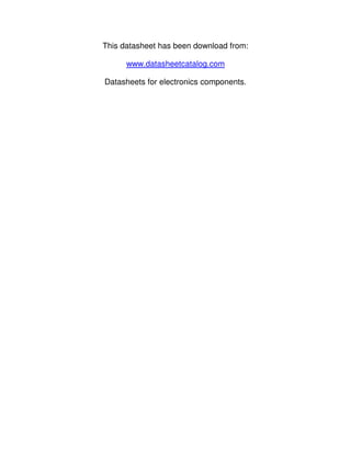
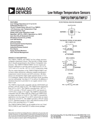
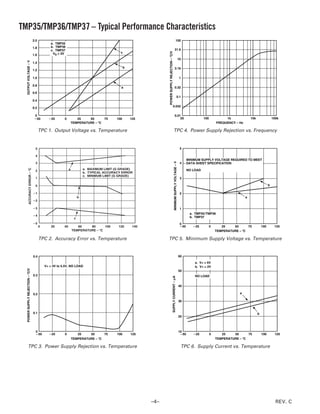
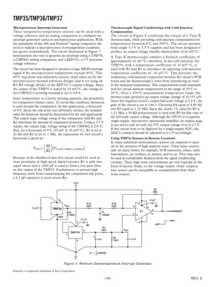
The document describes low voltage temperature sensors. It provides specifications for the TMP35, TMP36, and TMP37 sensors, which output a voltage linearly proportional to temperature. Key features include low voltage operation from 2.7-5.5V, accuracy of ±1-2°C, and low power consumption of less than 50μA. The sensors are available in small surface mount packages and are suitable for temperature monitoring in various applications.


![TMP35/TMP36/TMP37
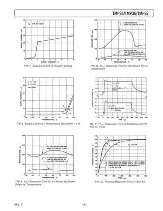
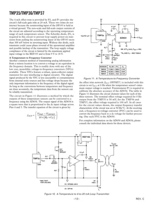
OUTLINE DIMENSIONS
3-Pin Plastic Header-Style Package [TO-92] 8-Lead Standard Small Outline Package [SOIC]
(TO-92) Narrow Body
Dimensions shown in inches and (millimeters) (RN-8)
Dimensions shown in millimeters and (inches)
0.205 (5.21) 5.00 (0.1968)
0.135
(3.43) 0.175 (4.45) 4.80 (0.1890)
MIN
8 5
0.210 (5.33) 4.00 (0.1574) 6.20 (0.2440)
0.170 (4.32) 3.80 (0.1497) 1 4 5.80 (0.2284)
SEATING 0.050
PLANE (1.27)
MAX 1.27 (0.0500) 0.50 (0.0196)
1.75 (0.0688) ؋ 45؇
BSC 0.25 (0.0099)
0.25 (0.0098) 1.35 (0.0532)
0.019 (0.482)
0.500 SQ 0.10 (0.0040)
(12.70) 0.016 (0.407)
MIN 0.51 (0.0201) 8؇
COPLANARITY 0.33 (0.0130) 0.25 (0.0098) 0؇ 1.27 (0.0500)
0.10 SEATING 0.41 (0.0160)
PLANE 0.19 (0.0075)
COMPLIANT TO JEDEC STANDARDS MS-012AA
0.055 (1.40) CONTROLLING DIMENSIONS ARE IN MILLIMETERS; INCH DIMENSIONS
0.105 (2.66) 0.045 (1.15) (IN PARENTHESES) ARE ROUNDED-OFF MILLIMETER EQUIVALENTS FOR
0.095 (2.42) REFERENCE ONLY AND ARE NOT APPROPRIATE FOR USE IN DESIGN
0.115 (2.92)
0.080 (2.03)
0.165 (4.19)
0.115 (2.92) 1 2 3
0.125 (3.18)
0.080 (2.03) 5-Lead Plastic Surface-Mount Package [SOT-23]
(RT-5)
BOTTOM VIEW
Dimensions shown in millimeters
COMPLIANT TO JEDEC STANDARDS TO-226AA
CONTROLLING DIMENSIONS ARE IN INCHES; MILLIMETERS DIMENSIONS 2.90 BSC
(IN PARENTHESES) ARE ROUNDED-OFF EQUIVALENTS FOR
REFERENCE ONLY AND ARE NOT APPROPRIATE FOR USE IN DESIGN
5 4
1.60 BSC 2.80 BSC
1 2 3
PIN 1
0.95 BSC
1.90
1.30 BSC
1.15
0.90
1.45 MAX
10؇
0.15 MAX 0.50 0؇ 0.60
SEATING 0.22
0.30 PLANE 0.45
0.08 0.30
COMPLIANT TO JEDEC STANDARDS MO-178AA
Revision History
Location Page
10/02—Data Sheet changed from REV. B to REV. C.
Deleted text from Commentary on Long-Term Stability section . . . . . . . . . . . . . . . . . . . . . . . . . . . . . . . . . . . . . . . . . . . . . . . . . . . 13
Update OUTLINE DIMENSIONS . . . . . . . . . . . . . . . . . . . . . . . . . . . . . . . . . . . . . . . . . . . . . . . . . . . . . . . . . . . . . . . . . . . . . . . . 14
–14– REV. C](https://image.slidesharecdn.com/32847740tmp3567c-121208083757-phpapp02/85/32847740-tmp35-6_7_c-14-320.jpg)