This document discusses signal integrity improvement in transition minimized differential signaling (TMDS) links. It provides background on digital visual interface (DVI) specifications and TMDS link architecture. A key part of TMDS links is the use of source termination to improve signal integrity by reducing rise times on the transmitted signals. The document presents simulation and measurement results showing that adding a 100-ohm source termination to the TMDS transmitter eliminates noise issues seen at high data rates.


![CHAPTER
INTRODUCTION
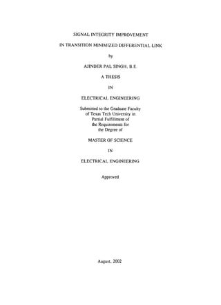
A Liquid Crystal Display (LCD) monitor like a conventional Cathode Ray Tube
monitor (CRT) is used to display graphics data from a Personal Computer (PC). LCD
monitors are fast becoming popular because they have great space and energy saving
advantages [1].
Figure 1.1 Flat Screen Monitor [2]
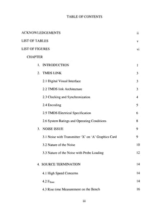
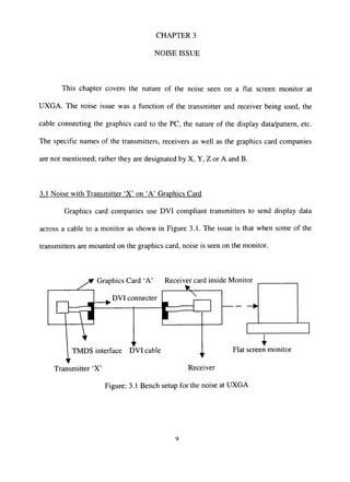
Graphics data is sent over a cable by a transmitter mounted on a graphics card to a
receiver residing in an LCD monitor via a cable [3] as shown in Figure 1.2.
Graphics Card Receiver card inside Monitor
Connector
TMDS interface cable
Transmitter
Flat screen monitor
Receiver
Figure 1.2 Link Connecting PC to LCD monitor](https://image.slidesharecdn.com/526f21eb-27c8-404e-87a5-360ffb83dd2d-150531180224-lva1-app6892/85/31295017084244-1-8-320.jpg)
![The specifications or standards that govern the connection of an LCD monitor to
the Personal Computer (PC) have been developed by the Digital Display Working Group
and are described in the Digital Visual Interface (DVI) specification [3], revision 1.0,
4/2/99.
The communication protocol followed to send graphics data between the
transmitter (TX) and the Receiver (RX) is defined as Transition Minimized Differential
Signaling (TMDS) [3]. TMDS protocol converts high frequency encoded graphics data to
Differential, DC balanced, low frequency code that reduces the loading of the
transmission line/link connecting the TX and the RX. Differential coding helps in EMI
reduction and ground bounce [4].
Graphics data can be clocked at frequencies from 25 MHz to 165 MHz depending
on the resolution of the LCD monitor [5, 6]. ta this thesis, a noise issue that was
encountered at 165MHz that is Ultra Extended Graphics Array Resolution is discussed.
In the second chapter, the DVI specifications as well as TMDS link architecture are
discussed in details. Chapter 3 covers the nature of the noise observed on a flat-screen
monitor at UXGA. Chapter 4 covers the transmission line concerns in the TMDS link
specifically the fast rise times of the TMDS signals as well as how a source termination
in addition to the far end termination helped in eliminating the noise issue. Chapter 5
provides a conclusion to the work and provides future directions for research.](https://image.slidesharecdn.com/526f21eb-27c8-404e-87a5-360ffb83dd2d-150531180224-lva1-app6892/85/31295017084244-1-9-320.jpg)
![CHAPTER 2
TMDS LINK
2.1 Digital Visual Interface
The Digital Visual Interface (DVI) specification describes a high-speed digital
connection for visual data type that is display technology independent [3]. The interface
is primarily focused at providing a connection between a computer and a display device.
The DVI specifications were defined by the Digital Display Working Group comprising
of companies like Silicon Image, Intel etc. The main characteristics of the DVI link are:
• Content remains in the loss-less digital domain from creation to consumption. No
loss involved in Digital to Analog conversion of the data.
• Display technology independence. It can support both Thin Film Transistor as
well as Dual Scan Twisted Nematic Displays.
• Plug and Play through hot plug detection. The operating system reads the
specifications of the monitor and activates the link hence the monitor can be
plugged or removed from the PC anytime.
2.2 TMDS link Architecture
A TMDS transmitter [3] encodes and serially transmits an input data stream over
a TMDS link to a TMDS receiver as shown in Figure 2.1. The transmitter contains three
identical encoders, each driving one serial TMDS data channel. The input to each
encoder is two control signals and eight bits of Red, Green and Blue pixel data.](https://image.slidesharecdn.com/526f21eb-27c8-404e-87a5-360ffb83dd2d-150531180224-lva1-app6892/85/31295017084244-1-10-320.jpg)
![Depending on the state of the Data Enable (DE), the encoder will produce 10-bit TMDS
characters either from the two control signals or from the eight bits of pixel data. The
input data stream contains pixel and control data. The transmitter encodes either the pixel
data or control data on any given input clock cycle, depending on the state of the data
enable signal DE. The active data enable signal indicates that pixel data is to be
transmitted. The control (pixel) data is ignored when the pixel (control) data is
transmitted. At the TMDS receiver, the recovered pixel (control) data may transition only
when DE is active (inactive).
_ ^_ R,
. . . . . . . : - . _ iireanInput Straams Streams
"^ r "^^ r
h,
rnpul N
Format
1InputInHrtaoeLayer
DF ^
l^het Data ti4 bits) ''
Control Oala (6 b,ts)
CLK ,
i
c
s
a
s
', Channel 1 J ^
^ C h a n n e l ^ / ^
/ ( Channel C) ^.
"PUJTPata <24 S i i r ^ g
C^yfliol Data (6 tali) ';
a.^
Output
Fofmat
S^BteTM.D.S.Da.aUn. ^•'''i£^^'^
Figure 2.1 TMDS Link Architecture [3]
2.3 Clocking and Svnchronization
A TMDS receiver receives a clock reference from a DVI transmitter [3] that has a
period equal to the pixel time, Tpix. The TMDS encoded data contains 10 bits per 8-bit
pixel; this implies that the serial bit rate is 10 times the pixel rate. For example, the
required pixel rate to support an UXGA resolution with 60Hz refresh rate is 165 MHz;
hence, the TMDS data bit rate is 1.65Gb/s.
The TMDS receiver must determine the location of the character boundaries in
the serial data streams. Once character boundaries are established on all data channels.](https://image.slidesharecdn.com/526f21eb-27c8-404e-87a5-360ffb83dd2d-150531180224-lva1-app6892/85/31295017084244-1-11-320.jpg)
![the receiver is defined to be synchronized to the serial streams and may recover TMDS
characters from the data channels for decoding. The TMDS data stream provides periodic
cues for decoder synchronization. The TMDS characters selected to represent pixel data
contain five or fewer transitions, while the TMDS characters selected to represent the
control data contain seven or more transitions. The high transition content of the
characters transmitted during the blanking period form the basis for the character
boundary synchronization at the decoder.
2.4 Encoding
A TMDS data channel [3] is driven with a continuous stream of 10-bit TMDS
characters. During the blanking interval there are four distinct characters that are
transmitted, which map directly to the four possible states of the two input control signals
input to the encoder. During active data, when each 10-bit character contains eight bits of
pixel data, the encoded character provides an approximate DC balance as well as
reduction in the number of transitions in the data stream. The encode process for the
active data period can be viewed in two stages. The first stage produces a transition-
minimized nine-bit code word from the input eight bits. The second stage produces a 10-
bit code word, the finished TMDS character that will manage the overall DC balance of
the transmitted stream of characters. The nine-bit code word produced by the first stage
of the encoder is made up of an eight-bit representation of the transitions found in the
input eight bits, and a one-bit flag to indicate which of the two methods was used to
describe the transitions as explained. In both cases, the least significant bit of the output](https://image.slidesharecdn.com/526f21eb-27c8-404e-87a5-360ffb83dd2d-150531180224-lva1-app6892/85/31295017084244-1-12-320.jpg)
![matches the least significant bit of the input. With the starting value established, the
remaining seven bits of the output word is derived from sequential exclusive OR (XOR)
or exclusive NOR (XNOR) functions of each bit of the input with the previously derived
bit. The choice between the XOR and XNOR logic is made such that the encoded values
contain the fewest possible transitions, and the ninth bit of the code word is used to
indicate whether XOR or XNOR functions were used to derive the output code word.
Decoding the nine-bit code word is simply a matter of applying either XOR or XNOR
gates to the adjacent bits of the code, with the least significant bit passing from decoder
input to decoder output unchanged.
The second stage of the encoder during active data periods on the interface
performs an approximate DC balance on the transmitted data stream by selectively
inverting the eight data bits of the nine-bit code words produced by the first stage. A
tenth bit is added to the code word, to indicate where the inversion has been made. The
encoder determines when to invert the next TMDS character based on the running
disparity between zeroes and ones that it tracks in the transmitted stream. If too many
ones have been transmitted and the input contains more ones than zeroes the code word is
inverted.
2.5 TMDS Electrical Specification
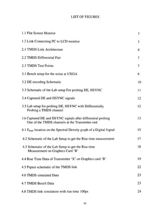
A conceptual schematic of a TMDS differential pair [3] is shown in Figure 2.2.
The TMDS technology uses current drive to develop a low voltage differential signal at
the receiver side of the DC-coupled transmission line. The link reference voltage AVCC](https://image.slidesharecdn.com/526f21eb-27c8-404e-87a5-360ffb83dd2d-150531180224-lva1-app6892/85/31295017084244-1-13-320.jpg)
![sets the high voltage level of the differential signal, while the current source of the
transmitter and the termination resistance of the receiver determine the low voltage level.
The termination resistance, Rjand the characteristic impedance of the cable, ZQ should be
matched.
T r a n s m i t t e r
Cucrent_4i')
Sourco ~^-'
t) • a
V
Receiver
Figure 2.2 TMDS Differential Pair [3]
Signal test points for a TMDS link are shown in Figure 2.3. The first test point
TPl, at the pins of the TMDS transmitter, is not utilized for testing under the
specifications since they are difficult to access. Rather, the transmitter is tested at TP2,
which includes the network from the transmitter to the connector as well as the connector
to the cable assembly. The input to the receiver is similarly described by signal testing at
TP3 rather than at TP4, the pins of the receiver. Hence, the link testing is reduced to
measurements at only two test points.
©
Transmitter
Network
-<^
_^_
i
Receiver
Network
Figure: 2.3 TMDS Test Points [3]](https://image.slidesharecdn.com/526f21eb-27c8-404e-87a5-360ffb83dd2d-150531180224-lva1-app6892/85/31295017084244-1-14-320.jpg)
![2.6 System Ratings and Operating Conditions
Maximum ratings of a TMDS interface [3] are specified in Table 2.1. Exceeding
these limits may damage the system. The required operating conditions of the TMDS
interface are specified in Table 2.2.
Table 2.1 Maximum Rafings of the TMDS link [3]
Item
Termination Supply Voltage, AVj,
Signal Voltage on Any Signal Wire
Common Mode Signal Voltage on Any Pair
Differential Motle Signal Volt^eon Any Pair
Termination Resistana
StorageTemperature Range
Value
4.0V
•0.5 to 4.0V
-0.5to4.0V
t33V
0 Ohms to Open Cireuit
-40 to 130 degrees Centigrade
Table 2.2 Required Operating conditions of
TMDS link [3]
Ittm Vahe ____,.
Tenranatinn SupplyVoltage, K 3.3V, ii%
TemnatioflResists 50(te,±10%
OperatingTenyeralureRange 0to7()degreesCeniipk
Hence, after a description of basic terms like DVI, TMDS and TMDS
architecture, the next chapter covers the nature of the noise issue seen on a LCD monitor
at UXGA resolution.](https://image.slidesharecdn.com/526f21eb-27c8-404e-87a5-360ffb83dd2d-150531180224-lva1-app6892/85/31295017084244-1-15-320.jpg)
![However, the graphics card can send the data clocked at pixel clock frequencies
ranging from 25MHz to 165MHz depending on the resolution of the monitor but the
noise was mainly seen when the pixel frequency was 165MHz that is the UXGA pixel
clock frequency.
To identify whether the noise was graphics card related or due to the specific
transmitter, the transmitter was mounted on a different graphics card 'B'. The observation
was that there was no noise on the monitor at UXGA. Hence, the first indication was that
the noise was extrinsic to the transmitter and was being generated in the link that was
connecting the transmitter and the receiver.
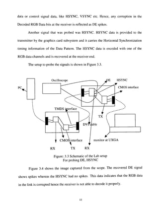
3.2 Nature of the Noise
To identify the nature of the noise two main signals. Data Enable (DE) and
HSYNC were probed at the receiver end [10] as shown in Figure in 2.4. The DE signal is
encoded with all three Red Green Blue (RGB), data channels [3] as shown in Figure 3.2.
f-.RMIT-ni
<~ri ' ^ ^ 1
BFrHTOf
^S^
Figure 3.2 DE encoding Schematic [3]
The DE signal indicates to the receiver whether the data in the TMDS link, that is
the link connecting the transmitter and receiver is a valid Red, Green and Blue (RGB)
10](https://image.slidesharecdn.com/526f21eb-27c8-404e-87a5-360ffb83dd2d-150531180224-lva1-app6892/85/31295017084244-1-17-320.jpg)
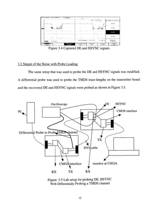
![As shown in Figure 3.6 the DE signal showed no spikes. This data indicates that
the probing of the TMDS channel with a probe could affect the data in two ways [11].
• The probe can slow down the rise times of the signals
• The probe can filter the high frequency noise components in the TMDS
link. Hence, the signal integrity of the transmitted data improves.
!Rk R u n : Ici.nMS/s Sii nip I,
~^ A B.v-,..,w.>
A: 3,72 V
®: -2.52 V
S^^vt*"
—•A ".y-J^iV •>*'-
'.X^'^^f^i,,A;'',s-s-,f^i..Jt i.^^*^--*.^.—„ i.^^^^(j.«y^ WA.'.-'rf^A^''i^i^'%-
IWB -^-oov
N."/rk . r^ri. j ^ ^ ^- y—^-4^ ,
MS.OOMS n , S r •1.64V^ - m o r e -
l o t 2
TVpe Couplititj 5lopi'
y
tevfj I Mode
S.
Htiltlnfl
Figure 3.6 Captured DE and HSYNC
Signals after Differential probing one of the
TMDS channels at the Transmitter end
Hence, the initial investigation indicated that the noise was due to the corruption
of the RGB data in the link. The next step was to investigate the characteristics of the
signals as well as the components that made up the entire link that included DVI cable,
connector, trace-lengths, etc.
13](https://image.slidesharecdn.com/526f21eb-27c8-404e-87a5-360ffb83dd2d-150531180224-lva1-app6892/85/31295017084244-1-20-320.jpg)
![CHAPTER 4
SOURCE TERMINATION
Since the initial investigation into the nature of the noise indicated, that the
characteristics of the TMDS signals carrying the RGB display data needed to be studied.
Hence, the first step was to study the electrical characteristics of the signals specifically
at UXGA as prescribed by the DVI specifications.
4.1 High Speed Concerns
Two important parameters from the DVI specifications raised the high-speed
concerns that could be the possible source of noise [3].
• The first major concern referring to the DVI specifications was the very fast Rise
and Fall Time (75ps-240ps).
• The second concern was the fast-serialized bit rate at UXGA and the
corresponding reduction in timing margins for jitter etc.
Fast rise and fall times raise issues related to transmission lines like, reflections and
ringing, as explained in Secdon 4.2.
4.2 FKn..
Most energy in digital pulses is concentrated below a frequency defined as the
knee frequency. Figure 4.1 illustrates the spectral power density of a digital signal. It
shows a negative 20dB/decade slope from Fdock to the frequency marked as Fknee- Beyond
14](https://image.slidesharecdn.com/526f21eb-27c8-404e-87a5-360ffb83dd2d-150531180224-lva1-app6892/85/31295017084244-1-21-320.jpg)
![Fknee, the spcctrum rolls off faster than 20dB/decade. The knee frequency of any digital
signal is directly related to the rise and fall time of its digital edges as defined by
Equation 4.1 [11].
Fknee =
Tr
(4.1)
Fknee = frequency below which most energy in digital pulses concentrates
Tr = pulse Rise time
Ctoi'k .'•cic 33 dB/dfcadc
conliMes up lo
ktise rrfqijcnc;
•sps!
5S,3li;ud»
i!! (Iliv
nO;.'.n of '.hi
(."iiMli rnU'
?'t.<ix(:). relalivf
,'.; knee
(r^BWic?: ;xc;ruK
is U ii bdow
slrjijhl sJOK
Figure 4.1 Fknee location on the Spectral Density
Graph of a Digital Signal [11]
Fast rise times push Fknee higher. Longer rise times push Fknee lower and for any
circuit element to pass a digital signal undistorted it should have a flat frequency response
up to and including Fknee- From the system level point of view as rise times, become fast.
15](https://image.slidesharecdn.com/526f21eb-27c8-404e-87a5-360ffb83dd2d-150531180224-lva1-app6892/85/31295017084244-1-22-320.jpg)
![the behavior of passive circuit elements becomes critical. These passive circuit elements
may include the wires, circuit boards, and integrated-circuit packages that make up a
digital product. At low speeds, passive circuit elements are just part of product's
packaging. At higher speed, they directly affect electrical performance and can cause
ringing and reflecfions in the link.
Rise times of a signal define whether a given system of conductors for example
circuit board traces will act as a lumped system or a distributed system [11]. If the system
size is smaller than one-sixth of the electrical length of the fastest electrical feature
(which in this case is the rise time of the signal), the system is classified as a lumped
system otherwise it is considered as a distributed system. This means that the parasitic
capacitance or inductance like the bond wire etc. load the signals. The next step was to
measure the rise time of the signals using bench test equipment.
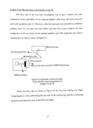
4.3 Rise Time Measurement on the Bench
A rise time measurement was taken as shown in Figure 4.2. The main limitation
when measuring the rise times was the bandwidth of the oscilloscope and the
oscilloscope probe. A lower bandwidth probe slurs out and slows down both the rise
times of the digital signals [11]. Ideally, the oscilloscope rise time should be less than one
fifth the rise time of the Device under Test (DUT).
The reading from the automated measurement displayed 166ps. According to the
specifications available, the rise time of the oscilloscope is 84ps and the rise time of the
16](https://image.slidesharecdn.com/526f21eb-27c8-404e-87a5-360ffb83dd2d-150531180224-lva1-app6892/85/31295017084244-1-23-320.jpg)
![oscilloscope probe is 112ps. Hence, rise time of the Device Under Test (DUT) [11] from
Equation 4.2 [11] was 90ps, approximately.
Rise-composite — 1 scope + 1 probe + 1 DUT (4.2)
Hence, this data indicated that the measured rise time that was 90ps was at the
low end of the DVI specification for the rise and fall times (75-240ps) [3, 5 and 6].
However, the main limitation in this reading was the rise time of the oscilloscope.
Oscilloscope
Oscilloscope Probe
Receiver EVM Board
DVI connecter
&
TMDS interface DVI cable Flat screen monitor
TX Receiver
Figure 4.2 Schematic of the Lab Setup
To get the Rise time measurement
17](https://image.slidesharecdn.com/526f21eb-27c8-404e-87a5-360ffb83dd2d-150531180224-lva1-app6892/85/31295017084244-1-24-320.jpg)
![iA; 78SI11V
ica: 3.OSS V
C3 Rise
29S.1P5
H 297.3|)
(T s.s:ip
a i l i 200mV mm-cf>rr 23 Mar 20
17:33:-10
Figure 4.4 Rise Time Data of Transmitter 'X' on
Graphics card 'B'
The main aspect of this initial investigation was that slower rise times as in the
case of the Transmitter 'X' mounted on the graphics card 'B', seemed to lead to the
elimination of noise on the screen/monitor.
The reason for the slow rise times was that the graphics card 'B' had internally
routed TMDS traces as compared to EVM boards or graphics card 'A', which had
externally routed TMDS traces. When the traces are routed between two ground planes
the electric field stays in the board yielding an effective dielectric constant of 4.5 hence
signals propagate more slowly [11]. Traces lying on the outside surface of the PCB board
share their electric field between air on one side and PCB board (FR4) material on the
other side yielding an effective dielectric constant 1-4.5.
Hence, outer layer PCB traces are always faster than the inner traces. Hence, this
data indicated that if the rise and fall times of the TMDS signals are slowed down the
noise can be eliminated.
19](https://image.slidesharecdn.com/526f21eb-27c8-404e-87a5-360ffb83dd2d-150531180224-lva1-app6892/85/31295017084244-1-26-320.jpg)
![4.5 TMDS Link Simulation
Since the rise time of the oscilloscope was the limiting factor in probing the
TMDS signals, simulation of the TMDS link was done to see the artifacts on the signals
that could be the cause of the noise. Oread Pspice 9.1 was used to model the TMDS link
pair that connects the transmitter and the receiver.
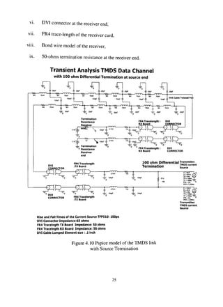
4.6 Features of the Pspice Model
Referring to Figure 4.5 the Pspice model of the TMDS link basically
characterized the transmission line effects like ringing, reflections, parasitic capacitive
and inductive loading encountered by the TMDS signals [3, 11].
The signals originate from the current drivers of the transmitter. The sequence in
which they are loaded is described as follows [5, 6, 9, 10 . 11 and 15].
i. Bond wire model of transmitter,
ii. FR4 trace-length of the graphics card,
iii. DVI connector at the transmitter end,
iv. DVI cable,
V. DVI connector at the receiver end,
vi. FR4 trace-length of the receiver card,
vii. Bond wire model of the receiver,
viii. 50-ohms termination resistance at the receiver end.
The DVI connector on the transmitter and the receiver side was modeled by a
transmission line with a characteristic impedance 65 ohms, this was to introduce
20](https://image.slidesharecdn.com/526f21eb-27c8-404e-87a5-360ffb83dd2d-150531180224-lva1-app6892/85/31295017084244-1-27-320.jpg)
![impedance discontinuity from the characteristic impedance of 50 ohms of the trace length
and the 50-55 ohms impedance of the DVI cable. This data was based on the TDR (Time
Domain Reflectometry) measurements.
The lumped element size (described in Section 4.2) of the DVI, cable was based
on the Equation 4.3 [11].
L - ^ (4.3)
Where L = Length of the rising edge, in,
Tr = Rise time, ps,
D = Delay, ps/in.
For the coaxial DVI cable, the value of Delay is 129ps/in [11]. The rise time of
the TMDS signals used was 90ps (as indicated in Section 4.3). Hence, the length of the
rising edge was calculated as 0.69 inches. For a system of conductors to behave in a
lumped fashion, it needs to be smaller than one-sixth of the electrical length of the fastest
electrical feature, which is the rise time of the TMDS signals, therefore DVI cable length
of 0.1 inch is considered as a limped element. The values of the DVI cable used in the
Pspice model are:
Inductance = 0.75nH/0.1 inch,
Capacitance= 0.22 pF/0.1 inch,
Resistance= 0.8m ohms/0.1 inch.
The values of the bond wire model in the transmitter and receiver chips used in
the Pspice model are [16]:
Inductance = 2nH,
21](https://image.slidesharecdn.com/526f21eb-27c8-404e-87a5-360ffb83dd2d-150531180224-lva1-app6892/85/31295017084244-1-28-320.jpg)
![Resistance= 0.154 ohms,
Capacitance= 0.104pF.
Transient Analysis TMDS Data Channel
with 100 ohm Differential Termination at source end
-<WV ( " V Y Y ^ .
8m 75nH
r]
~0
8m 75nH em 75nH
n22pF
Bm 75nH
n • 0
J . 8m 75nH
- i 22pF
'^^t^ - p iMpr -J. iMph = 154pF = :
'"'^^—h VW—'^'•^''TM_^—,^—/-YYYvL 1/^—nnnrJ—VW '">'YY-> U
rSnH i . eir. 7 5 * 1 »m 7511H 1 em .TSnH 1 .8m 75nH 1
4 : ^ f - i i2pF i 2!PF i 22pF i
DVI Cable Twisted Pa
Termination
Resistance
Recover
end
J.
FR4 Tracelengtii: DVI
1•0
..
i
~o
-WW—
, 5 4 1 ,
" ^
DVI
3 3 V - ± - =" ' ^ J 0 4 p F
i Termination
" Resistance
Receiver
end
FR4 Tracelengtii
:TX Board
• 0
RX Board CONNECTOR
~0 " 0 " 0 " 0
^ ,Q4pF V — ' / — i i _ _ V — ? > — r _
-0 -0 "0
FR4 Tracelength: DVI
RX Board CONNECTOR
CONJUfCTOR , ,
Transmiiter:
TMDS current
Source
± 27nH
"—" IMpF
• 0 •0
^^ft-^t^^
11= 0mA 1 12
12 = 20mA (T
TD = Ons V t y
TR = lOOps _ J _
TF= loops —
PW = Ins 0
P£R = 2 200fB
X
2 7 *
DVI
CONNECTOR F"* Tracelength
:TX Board
• 0
,1=20mA
,2 = aiiiA
TD = Ofs
TR = ,0Ops
TF= loops —
PW.lns y
PER = 2500ns
Transmiiter:
TMDS current
Source
Rise and Fall Times of the Current Source TFP510: lOOps
DVI Connector Impedance:65 ohms
FR4 Tracelngth TX Board Impedance: 50 ohms
FR4 Tracelngth RX Board Impedance: 50 ohms
DVI Cable Lumped Element size: .1 inch
Figure 4.5 Pspice schematic of the TMDS link
The rise times of the TMDS signals was set at lOOps. A current source with high
input impedance was used to model the TMDS drivers as per the specification. The
22](https://image.slidesharecdn.com/526f21eb-27c8-404e-87a5-360ffb83dd2d-150531180224-lva1-app6892/85/31295017084244-1-29-320.jpg)
![termination at the far end that is at the receiver end was set at 50 ohms to match the
impedance of the transmission line [3].
From Figures 4.6 and 4.7 a comparison was made between the data collected from
the Pspice model and the bench measurements. This data reflected that the Pspice model
was close to the actual lab setup.
Figure 4.6 TMDS simulated Data Figure 4.7 TMDS Bench Data
4.7 Effect of Rise Time in the Pspice Model
Once the Pspice model of the TMDS link was developed, it was characterized for
different rise times. Since the DVI specifications for the rise times of the TMDS signals
is between 75ps to 240ps [3], the simulations were done to compare the signal integrity at
lOOps and 240ps as shown in Figures 4.8 and 4.9.
Slower rise time signal had a larger peak-to-peak value with less ringing. Peak-
to-peak value of the signal amplitude was 460mV at lOOps rise time. Peak-to-peak value
of the signal amplitude was 670mV at 240ps rise time.
23](https://image.slidesharecdn.com/526f21eb-27c8-404e-87a5-360ffb83dd2d-150531180224-lva1-app6892/85/31295017084244-1-30-320.jpg)
![Thus this simulation result indicated that the issue could indeed be related to
transmission line effects like ringing and reflections in the TMDS link and slow rise
times did help in reducing these effects.
^
i
•».-.. 1 l-..~..l
4
! -
1ft "*'/(—*^!»^By i ' ^ " ' - ' ^ ' , _^„ J3
,. 1 .,
[.X,.*.^w.*;,N«.y
Figure 4.8 TMDS link simulation
With rise time lOOps
Figure 4.9 TMDS link simulation
with rise time 240ps
4.8 Simulation with Source termination
A resistor of 100 ohms was added to the model at the transmitter end across the
positive and the negative signals of the differential pair as shown in Figure 4.10. The
logic behind using the source termination was to absorb the reflection at the source end in
addition to the far end that is the receiver end [11,12].
The sequence in which they are loaded is:
i. Bond wire model of transmitter,
ii. 100-ohm differential source termination,
iii. FR4 trace-length of the graphics card,
iv. DVI connector at the transmitter end,
V. DVI cable.
24](https://image.slidesharecdn.com/526f21eb-27c8-404e-87a5-360ffb83dd2d-150531180224-lva1-app6892/85/31295017084244-1-31-320.jpg)
![Referring to Figures 4.11 and 4.12, the simulated data showed that the fidelity of
the signal was much improved with 100-ohm termination with reduced reflections and
ringing.
Figure 4.11 TMDS link with
No Source Termination
Figure 4.12 TMDS link with
100-ohm Differential Source
Termination
4.9 Bench Verification of Source Termination
Bench Evaluation was done in two steps:
• 100 ohm termination was soldered at three differential TMDS data pairs that
are Red, Green and Blue [3] as shown in Figure 4.13. In this case no noise
was observed on screen
Transmitter
D ' D
Source
f L
XT'-
Dvi C*ML
-c
V
Receiver
Figure 4.13 Schematic of 100-ohm termination
In the TMDS model [3]
26](https://image.slidesharecdn.com/526f21eb-27c8-404e-87a5-360ffb83dd2d-150531180224-lva1-app6892/85/31295017084244-1-33-320.jpg)
![• In the second step, a 100 ohm resistor was soldered to only one of the TMDS
data pair and the other two pairs were left unsoldered. This was done to
compare the integrity of the two signals on the oscilloscope.
The setup for the test is shown in Figure 4.14. A pattern generator was used to
feed in vertical gray scale pattern to the transmitter card. A standard 2 meter DVI cable
was used to connect between the transmitter and the receiver card. Tektronix P6330 [ 16]
differential probe was used to probe the differential pair near the receiver end that
corresponds to test point TP4.
Pattern Generatoj-
Oscilloscope 7104
Oscilloscope Differential Probe P6330
Passilve Probe P6158
TMDS interface DVI cable Flat screen monitor
TX RX
(Recovered Clock- the eye is triggered on the Recovered Clock at the Receiver end
available at the ODCK pin)
Figure 4.14 Lab Setup for Verification of
Source Termination
27](https://image.slidesharecdn.com/526f21eb-27c8-404e-87a5-360ffb83dd2d-150531180224-lva1-app6892/85/31295017084244-1-34-320.jpg)
![The signal was characterized at 60MHz, 80MHz, 120MHz, and 162MHz pixel
clock frequencies. The main characteristic of the signal that was characterized was jitter.
Jitter is defined as the short-term variation of the significant instants of a digital signal
from their ideal positions in time. The Tektronix oscilloscope TDS7104 has an automated
tool that measures the peak-to-peak jitter [17].
The value of peak-to-peak jitter was compared in all the cases of the pixel clock
frequency characterized. The maximum allowable jitter on the edges at the receiver end
as per DVI specification [3] is in terms of the normalized time, as shown in Figure 4.15.
The minimum eye opening is 150mV and the time is normalized to one Tbu.
One Tbit duration is one-tenth of the clock period. For example, if the frequency of
operation is 162MHz UXGA [3 ,5, 6, 9 and 10], then one clock period is 6.16ns and since
10 bits of data is latched per clock cycle therefore one Tbn is 616ps. The allowable jitter
values are normalized accordingly based on Figure 4.15.
O.Q 025 0.30 0.70 0.75
Normalized Time
Figure 4.15 Signal Integrity at Receiver
End as per DVI Specification [3]
28](https://image.slidesharecdn.com/526f21eb-27c8-404e-87a5-360ffb83dd2d-150531180224-lva1-app6892/85/31295017084244-1-35-320.jpg)
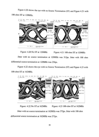
![Figure 4.16 shows the eye with no source termination (ST) and Figure 4.17 with
100-ohmSTat60MHz.
ffe E« yelicd Hoio/Acq Ir«
Tek FaslAtq Simple
r~ ~^ -
Figure: 4.16 No ST at 60MHz Figure: 4.17 100-ohm ST at 60MHz
Jitter with no source termination (ST)at 60 MHz was 350ps. Jitter with 100 ohm
differential source termination (ST) at 60MHz was 250ps.
Figure 4.18 shows the eye with no source termination (ST) and Figure 4.19 with
100-ohmSTat80MHz.
n « £d« V s n u J Hgt[!/Aog Tng Depby & J t o i ! M M ] i i e M ^ h U l i t w i Help
Tek FaflAcq Sample _ _ _ 29 hp 0 2 1 4 1 * ^ 3 _ _
Fie £ * VertcJ H»E/Aai Irig [Jiiplay £ i * « i i M e « j e H«ih j J S w i Ht^,
T(* F d t e i ) Sjmp* B H p r 02 5; 1647
>1
v : •
AV •
H':tft)
PV-Pk[Hi
• ^ : o m v
6;0ri¥
HOmV
28B7W*
2BOOP3
Sidl>v(Hil 4 i ; 7 ( s
Figure: 4.18 No ST at 80MHz Figure: 4.19100-ohm ST at 80MHz
Jitter with no source termination at 80MHz was 430ps. Jitter with 100 ohm
differential source termination at 80MHz was 260ps.
29](https://image.slidesharecdn.com/526f21eb-27c8-404e-87a5-360ffb83dd2d-150531180224-lva1-app6892/85/31295017084244-1-36-320.jpg)
![Jitter comparison
400
^ 350 ^
Q. 300
Q. 250
Q.
_ 200
<u
.« 150100
50
0 -
m-
•
--M
— # —
''*,
— - 4 — '•V^^
„.,„ „ . .*. •-'>-».»,-..,.
-Source Termination
-No Source
Termination
Allowable jitter DVI
spec
60 80 120
Frequency MHz
162
Figure 4.24 Jitter Comparison Chart
Figure 4.24 shows the comparison of the jitter values with and without source
termination with DVI specification as a reference. The comparison was done on one side
of the eye, referring to Figure 4.15 the allowable limit on one side of the eye is 25% of
the Tbit [3]. The histogram values generated from the oscilloscope for the peak-to-peak
jitter were divided by two to get the jitter value on one side of the eye for the comparison.
4.10 Mathematical Analysis
In this section, mathematical analysis is done on how adding a source termination
helps in reducing the reflections [11]. For example, when a signal is impressed upon a
transmission line, a fraction of the full source voltage propagates down the line. The
fraction is a function of frequency and is called A(w), the input acceptance function. The
value of A(w) is determined by the source impedance Zs, the transmission line impedance
Zo as defined by Equation 4.4 [ 11 ].
ZO{w) (4.4)
A(w) =
Zs (w) + ZO(w)
31](https://image.slidesharecdn.com/526f21eb-27c8-404e-87a5-360ffb83dd2d-150531180224-lva1-app6892/85/31295017084244-1-38-320.jpg)
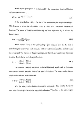
![also reflects back toward the source, in an endless cycle. The first signal to emerge from
the cable is attenuated by A (w), H, (w) and T (w) as defined by Equadon 4.9.
SO(u) = A{w)Hx{w)T(n) (4 9^
The second signal to emerge, after having reflected from both the far end and the
source end is attenuated by
51(w) = A{w)Hxiw)T(w)[R2iw)Rl{w)Hx(wy ] (4. ] O)
Successive emerging signals are characterized by
Sriw) = A{w)Hj<(w)T{w)[R2iw)m{w)Hxiwf]" (4. ] 1)
The sum of these signals is
5oo(vr) = ^^^^5«(H) (4.12)
The closed form equivalent to the above infinite sum is
5oo(w)= M^mMTM
-R2(w)R{w)Hx(wy
From Equations 4.7 and Equation 4.13, a resistor matching the characteristic
impedance at the far end should make the denominator one [11] and absorb the
reflections. However, in the case of the closely routed differential traces as in the case of
the TMDS signals the ideal value of termination resistance is not exacfly equal to the
impedance of the transmission line [18].
For example, two closely routed differential traces with characteristic impedance
Zo, having voltages V2 and VI can be considered. Since, they are differential, V2 = -VI.
VI causes a current II along trace 1 and V2 causes a current 12 along trace 2. The current
necessarily is derived from Ohm's Law, I = V/ZQ. Since it is a differential transmission
33](https://image.slidesharecdn.com/526f21eb-27c8-404e-87a5-360ffb83dd2d-150531180224-lva1-app6892/85/31295017084244-1-40-320.jpg)
![and the traces are closely routed together the current carried by Trace 1 (for example)
actually consists of 11 and K*I2 [18], where K is proportional to the coupling between
Trace 1 and 2. Hence, the net effect of this coupling is an apparent impedance (with
respect to ground) along Trace 1 equal to Z = Zo - Z12 where Z12 is caused by the
mutual coupling between trace 1 and trace 2. If trace 1 and 2 are far apart, the coupling
between them is very small, and the correct termination of each trace is simply Zo.
However, as the traces come closer together, and the coupling between them increases,
then the impedance of the trace reduces proportional to this coupling. This implies that
the proper termination of the trace (to prevent reflections) is Zo - Z12, or something less
than Zo.
Hence, the key factor here is that a termination resistor matching the characteristic
impedance of the transmission line (DVI specification) does not absorb all the reflections.
Moreover, since the TMDS drivers use a current source with a high output impedance,
the reflections (Equation 4.8) at the source end are large, which means that the signals
keep bouncing back and forth and cause jitter in the incoming data. However, a resistor
matching the impedance of the transmission line at the source end in addition to far end
absorbs most of the energy of the reflections.
Hence, the conclusion was that in case of the close differentially routed lines as in
the case of the TMDS signals the source termination in addition to the far end termination
helped in absorbing the reflections and the signal integrity improved.
34](https://image.slidesharecdn.com/526f21eb-27c8-404e-87a5-360ffb83dd2d-150531180224-lva1-app6892/85/31295017084244-1-41-320.jpg)
![REFERENCES
[I] Comparing Conventional CRT and Flat Panel LCD Monitors,
http://www.touchscreens.com/intro-displavtech.html
[2] Hitachi Displays website, http://www.hitachidisplavs.com
[3] Digital Visual Interface Revision 1.0, http://www.ddwg.org 1999.
[4] Inside Differential Signals, Cadence Community Educational Series, Dec.
2001 ,http://www.specctraquest.com/Downloads/InsideDiffSigals Green.qxd.
pdf
[5] Texas Instruments TI PanelBus Digital Transmitter, SLDS145A, http://www-
s.ti .com/sc/ds/tfp410.pdf, October 2001.
[6] Texas Instruments TI PanelBus Digital Receiver, SLDS120A, http://www-
s.ti.com/sc/ds/tfp401.pdf, March 2000.
[7] NVIDIA Graphics FAQ/Support website,
http://www.nvidia.com/view.asp?PAGE=support fags
[8] MATROX Graphics card support website,
http://www.matrox.com/mga/support/home.cfm
[9] Texas Instruments TI PanelBus Digital Transmitter, SLDS146, http://www-
s.ti.com/sc/ds/tfp510.pdf, January 2002.
[10] Texas Instruments TI PanelBus Digital Receiver, SLDS127A, http://www-
s.ti.com/sc/ds/tfp501.pdf, August 2001.
[II] Johnson H and Graham M. High-Speed Digital Design. Prentice-Hall, Upper
Saddle River, NJ, 1993.
[12]Ludwig R and Bretchko P RF Circuit Design. Addison Wesley Longman,
Singapore, 2001.
[13] Tektronix Oscilloscopes Home Page, http://www.tek.com/Measurement/cgi-
bin/framed.pl?Document=/Measurement/scopes/home.html&FrameSet=oscill
oscopes.
36](https://image.slidesharecdn.com/526f21eb-27c8-404e-87a5-360ffb83dd2d-150531180224-lva1-app6892/85/31295017084244-1-43-320.jpg)
![[14] Tektronix P6158 Probe Specifications, http://www.tek.com/Measurement/cgi-
bin/framed.pl?Document=http://www.tek.com/Measurement/Products/catalog
/p6158/order.html&FrameSet=accessories.
[15] Plastic Packages' Electrical Performance: Reduced Bond Wire Diameter,
Nozad Karim Amit P. Agrawal,
http://www.amkor.com/services/electrical/newabstr.pdf
[16] Tektronix P6330 Probe Specificafions, http://www.tek.com/Measurement/cgi-
bin/framed.pl?Document=http://www.tek.com/Measurement/Products/catalog
/p7330/eng/order.html&FrameSet=mbd.
[17] Tektronix website, Application Note, Performing Jitter Measurements, with
The TDS 700D/500D, Digital Phosphor Oscilloscopes,
http://www.tek.com/Measurement/App Notes/dpo/iittermeas/eng/55W 12048
l.pdf
[18]Impedance Terminations, What's the Value, Douglas Brooks, Printed Circuit
Design, a Miller Freeman publication, June 1999,
http://www.ultracad.com/terminations.pdf
[19] Vectors Technology Brief, Digital Visual Interface, May 2000,
h«p://www.dell.com/us/en/gen/topics/vectors 2000-dvi.htm
[20] LVDS Fundamentals, Fairchild Semiconductor Application Notes, December
2000, AN5017, http://www.fairchildsemi.com/an/AN/AN-5017.pdf
[21]Differential Signaling and Differential Transmission Lines,
http://www.chipcenter.com/n1tu/netsim/si/differential/diff article.html.
37](https://image.slidesharecdn.com/526f21eb-27c8-404e-87a5-360ffb83dd2d-150531180224-lva1-app6892/85/31295017084244-1-44-320.jpg)