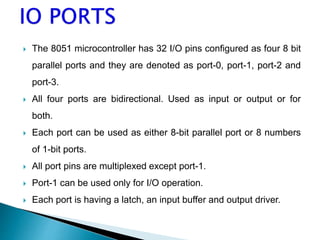
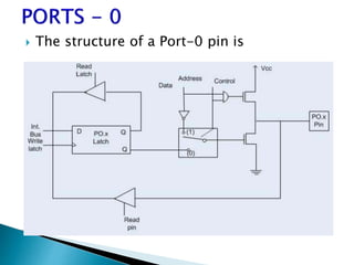
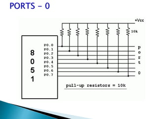
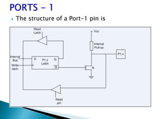
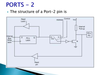
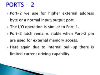
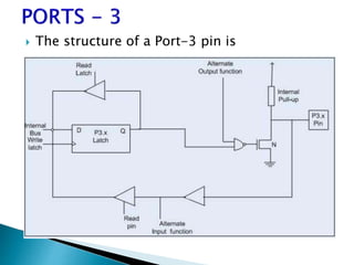
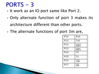
SRI KRISHNA COLLEGE OF ENGINEERING AND TECHNOLOGY
Kuniamuthur, Coimbatore, Tamilnadu, India
An Autonomous Institution, Affiliated to Anna University,
Accredited by NAAC with “A” Grade & Accredited by NBA (CSE, ECE, IT, MECH ,EEE, CIVIL& MCT)
18EE502-MICROCONTROLLERS
Module 1: 8051 Microcontroller
by
Mr.V.V.Vineeth
Assistant Professor
Department of Electrical and Electronics Engineering
8051: IO PORTS
Animation by
EnggClasses – YouTube Channel
Mr. Nair Vishal Vijay
Karunya Institute of Technology and
Sciences
Module 1: 8051 Microcontroller 15 Hrs
Overview of Microprocessors - 8051: Functional block diagram - Instruction
set - addressing modes – Interrupt structure - Timer – I/O ports – Serial
Communication, Simple programming - Key board and display interface –
Temperature control system - Stepper motor control.
Module 2: PIC Microcontroller 15 Hrs
PIC18FXXX: Architecture - Data and program memory organization -
Addressing modes - Instruction set - Move / Copy instructions, Arithmetic
instructions, Logic instructions, Branches instructions, Bit Manipulation
instructions, Table Read/Write instructions, Machine Control instructions –
Timers – Interrupt, ISR, priority.
Module 3: ARM Controller 15 Hrs
ARM7TDMI: Features – Block diagram – Architecture – Addressing modes
– Instruction set – Thumb instructions - Data processing instructions, Data
transfer instructions, Branch and control instructions, Register load and
store instructions, Multiple register load and store instructions, Status
register access instructions, Coprocessor instructions.
1. Kenneth Ayala, “The 8051 Microcontroller”, Cengage Learning
Publications, 2nd Edition, 2008.
2. John.B.Peatman , “ Design with PIC Microcontroller , Prentice hall,
2012.
3. Subrata Ghoshal, 8051 Microcontroller Internals, Instructions,
Programming and Interfacing, Second edition, Pearson Education Asia,
2014.
4. Myke Predko, “Programming and customizing the PIC microcontroller”,
Tata McGraw Hill Publishing Company Limited, Third Edition, 2008.
5. Steve Furber, ‟ ARM System –On – Chip architecture“, Addision
Wesley, 2009.
1. Muhammad Ali Mazidi, Janice Gillispie Mazidi, Rolin
McKinlay, ‘The 8051 Microcontroller and Embedded
Systems using Assembly and C’, Prentice Hall
Publications, 2nd Edition, 2008.
2. Krishna Kant, ‘Microprocessor and Microcontrollers’,
Eastern Company Edition, Prentice Hall of India, New
Delhi, 2nd edition,2013.
3. Joseph Yiu , ‘The Definitive Guide to the ARM Cortex-
M0’ Newnes – Elsevier, 2011.
4. Muhammad Tahir and Kashif Javed, ‘ARM
Microprocessor Systems - Cortex-M Architecture,
Programming, and Interfacing’, CRC Press, 2011.
 The 8051 microcontroller has 32 I/O pins configured as four 8 bit
parallel ports and they are denoted as port-0, port-1, port-2 and
port-3.
 All four ports are bidirectional. Used as input or output or for
both.
 Each port can be used as either 8-bit parallel port or 8 numbers
of 1-bit ports.
 All port pins are multiplexed except port-1.
 Port-1 can be used only for I/O operation.
 Each port is having a latch, an input buffer and output driver.
 The structure of a Port-0 pin is
 Port-0 can be used as a normal bidirectional
I/O port or it can be used for address/data
interfacing for accessing external memory.
 When the control is '0', the port can be used
as a bidirectional I/O port.
 When control is '1', the port is used for
address/data interfacing.
PORT 0 as an Input Port:
 Let us assume that control is '0'.
 When the port is used as an input port,
'1' is written to the latch.
 In this situation both the output
MOSFETs are 'off'.
 Hence the output pin have floats hence
whatever data written on pin is directly
read by read pin.
PORT 0 as an Output Port :
 To write 1 on pin of Port 0, a '1' written to
the latch which turns 'off' the lower FET
while due to '0' control signal upper FET
also turns off.
 Instead of logic '1' on pin, floating value will
be getting on the pin.
 So to convert that floating value into logic
'1‘, it is need to connect the pull up resistor
parallel to upper FET .
 To write '0' on port 0 pin, when '0' is written to the
latch, the pin is pulled down by the lower FET. Hence
the output becomes zero.
 When the control is '1', address/data bus controls the
output driver FETs.
 If the address/data bus (internal) is '0', the upper FET
is 'off' and the lower FET is 'on'. The output becomes
'0'.
 If the address/data bus is '1', the upper FET is 'on'
and the lower FET is 'off'. Hence the output is '1'.
 Hence for normal address/data interfacing (for
 The structure of a Port-1 pin is
 Port-1 dedicated only for I/O interfacing.
 When used as output port, not needed to
connect additional pull-up resistor like port
0. It have provided internally pull-up
resistor.
 The pin is pulled up or down through
internal pull-up when we want to initialize
as an output port.
 To use port-1 as input port, '1' has to be written
to the latch. In this input mode when '1' is
written to the pin by the external device then it
read fine.
 But when '0' is written to the pin by the external
device then the external source must sink
current due to internal pull-up.
 If the external device is not able to sink the
current the pin voltage may rise, leading to a
 The structure of a Port-2 pin is
 Port-2 we use for higher external address
byte or a normal input/output port.
 The I/O operation is similar to Port-1.
 Port-2 latch remains stable when Port-2 pin
are used for external memory access.
 Here again due to internal pull-up there is
limited current driving capability.
 The structure of a Port-3 pin is
 It work as an IO port same like Port 2.
 Only alternate function of port 3 makes its
architecture different than other ports.
 The alternate functions of port 3m are,
1.7_IO Ports (2).pptx

1.7_IO Ports (2).pptx

  • 1.
    SRI KRISHNA COLLEGEOF ENGINEERING AND TECHNOLOGY Kuniamuthur, Coimbatore, Tamilnadu, India An Autonomous Institution, Affiliated to Anna University, Accredited by NAAC with “A” Grade & Accredited by NBA (CSE, ECE, IT, MECH ,EEE, CIVIL& MCT) 18EE502-MICROCONTROLLERS Module 1: 8051 Microcontroller by Mr.V.V.Vineeth Assistant Professor Department of Electrical and Electronics Engineering 8051: IO PORTS
  • 2.
    Animation by EnggClasses –YouTube Channel Mr. Nair Vishal Vijay Karunya Institute of Technology and Sciences
  • 3.
    Module 1: 8051Microcontroller 15 Hrs Overview of Microprocessors - 8051: Functional block diagram - Instruction set - addressing modes – Interrupt structure - Timer – I/O ports – Serial Communication, Simple programming - Key board and display interface – Temperature control system - Stepper motor control. Module 2: PIC Microcontroller 15 Hrs PIC18FXXX: Architecture - Data and program memory organization - Addressing modes - Instruction set - Move / Copy instructions, Arithmetic instructions, Logic instructions, Branches instructions, Bit Manipulation instructions, Table Read/Write instructions, Machine Control instructions – Timers – Interrupt, ISR, priority. Module 3: ARM Controller 15 Hrs ARM7TDMI: Features – Block diagram – Architecture – Addressing modes – Instruction set – Thumb instructions - Data processing instructions, Data transfer instructions, Branch and control instructions, Register load and store instructions, Multiple register load and store instructions, Status register access instructions, Coprocessor instructions.
  • 4.
    1. Kenneth Ayala,“The 8051 Microcontroller”, Cengage Learning Publications, 2nd Edition, 2008. 2. John.B.Peatman , “ Design with PIC Microcontroller , Prentice hall, 2012. 3. Subrata Ghoshal, 8051 Microcontroller Internals, Instructions, Programming and Interfacing, Second edition, Pearson Education Asia, 2014. 4. Myke Predko, “Programming and customizing the PIC microcontroller”, Tata McGraw Hill Publishing Company Limited, Third Edition, 2008. 5. Steve Furber, ‟ ARM System –On – Chip architecture“, Addision Wesley, 2009.
  • 5.
    1. Muhammad AliMazidi, Janice Gillispie Mazidi, Rolin McKinlay, ‘The 8051 Microcontroller and Embedded Systems using Assembly and C’, Prentice Hall Publications, 2nd Edition, 2008. 2. Krishna Kant, ‘Microprocessor and Microcontrollers’, Eastern Company Edition, Prentice Hall of India, New Delhi, 2nd edition,2013. 3. Joseph Yiu , ‘The Definitive Guide to the ARM Cortex- M0’ Newnes – Elsevier, 2011. 4. Muhammad Tahir and Kashif Javed, ‘ARM Microprocessor Systems - Cortex-M Architecture, Programming, and Interfacing’, CRC Press, 2011.
  • 6.
     The 8051microcontroller has 32 I/O pins configured as four 8 bit parallel ports and they are denoted as port-0, port-1, port-2 and port-3.  All four ports are bidirectional. Used as input or output or for both.  Each port can be used as either 8-bit parallel port or 8 numbers of 1-bit ports.  All port pins are multiplexed except port-1.  Port-1 can be used only for I/O operation.  Each port is having a latch, an input buffer and output driver.
  • 7.
     The structureof a Port-0 pin is
  • 8.
     Port-0 canbe used as a normal bidirectional I/O port or it can be used for address/data interfacing for accessing external memory.  When the control is '0', the port can be used as a bidirectional I/O port.  When control is '1', the port is used for address/data interfacing.
  • 9.
    PORT 0 asan Input Port:  Let us assume that control is '0'.  When the port is used as an input port, '1' is written to the latch.  In this situation both the output MOSFETs are 'off'.  Hence the output pin have floats hence whatever data written on pin is directly read by read pin.
  • 10.
    PORT 0 asan Output Port :  To write 1 on pin of Port 0, a '1' written to the latch which turns 'off' the lower FET while due to '0' control signal upper FET also turns off.  Instead of logic '1' on pin, floating value will be getting on the pin.  So to convert that floating value into logic '1‘, it is need to connect the pull up resistor parallel to upper FET .
  • 12.
     To write'0' on port 0 pin, when '0' is written to the latch, the pin is pulled down by the lower FET. Hence the output becomes zero.  When the control is '1', address/data bus controls the output driver FETs.  If the address/data bus (internal) is '0', the upper FET is 'off' and the lower FET is 'on'. The output becomes '0'.  If the address/data bus is '1', the upper FET is 'on' and the lower FET is 'off'. Hence the output is '1'.  Hence for normal address/data interfacing (for
  • 13.
     The structureof a Port-1 pin is
  • 14.
     Port-1 dedicatedonly for I/O interfacing.  When used as output port, not needed to connect additional pull-up resistor like port 0. It have provided internally pull-up resistor.  The pin is pulled up or down through internal pull-up when we want to initialize as an output port.
  • 15.
     To useport-1 as input port, '1' has to be written to the latch. In this input mode when '1' is written to the pin by the external device then it read fine.  But when '0' is written to the pin by the external device then the external source must sink current due to internal pull-up.  If the external device is not able to sink the current the pin voltage may rise, leading to a
  • 16.
     The structureof a Port-2 pin is
  • 17.
     Port-2 weuse for higher external address byte or a normal input/output port.  The I/O operation is similar to Port-1.  Port-2 latch remains stable when Port-2 pin are used for external memory access.  Here again due to internal pull-up there is limited current driving capability.
  • 18.
     The structureof a Port-3 pin is
  • 19.
     It workas an IO port same like Port 2.  Only alternate function of port 3 makes its architecture different than other ports.  The alternate functions of port 3m are,