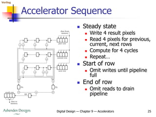
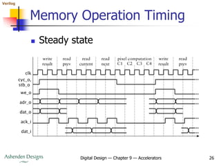
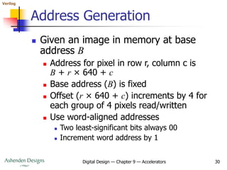
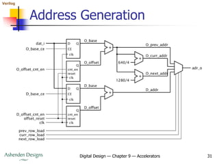
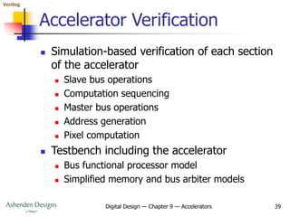
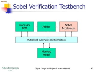
The document discusses accelerators for improving performance in digital systems. It describes how accelerators can perform operations in parallel to speed up algorithms. Key points include:
- Accelerators use custom hardware to perform parallel operations that would be too slow on a general-purpose processor.
- Amdahl's law describes how speeding up part of an algorithm affects the overall speedup achievable.
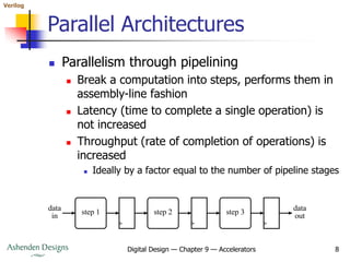
- Common parallel architectures include replication for independent data elements and pipelining to break computations into sequential steps.
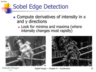
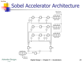
- The document then provides an example accelerator for edge detection in images using the Sobel algorithm. It describes the algorithm, data rates, memory bandwidth considerations, and pipeline architecture.
![Verilog
Digital Design — Chapter 9 — Accelerators 18
The Algorithm in Pseudocode
for (row = 1; row <= 478; row = row + 1) begin
for (col = 1; col <= 638; col = col + 1) begin
sumx = 0; sumy = 0;
for (i = –1; i <= +1; i = i + 1) begin
for (j = –1; j <= +1; j = j + 1) begin
sumx = sumx + 0[row+i][col+j] * Gx[i][j];
sumy = sumy + 0[row+i][col+j] * Gy[i][j];
end
end
D[row][col] = abs(sumx) + abs(sumy);
end
end](https://image.slidesharecdn.com/09accelerators-210924153936/85/09-accelerators-18-320.jpg)
![Verilog
Digital Design — Chapter 9 — Accelerators 27
Pixel Datapath
// Computation datapath signals
reg [31:0] prev_row, curr_row, next_row;
reg [7:0] O [-1:+1][-1:+1];
reg signed [10:0] Dx, Dy, D;
reg [7:0] abs_D;
reg [31:0] result_row;
...
// Computational datapath
always @(posedge clk_i) // Previous row register
if (prev_row_load) prev_row <= dat_i;
else if (shift_en) prev_row[31:8] <= prev_row[23:0];
... // Current row register
... // Next row register
function [10:0] abs (input signed [10:0] x);
abs = x >= 0 ? x : -x;
endfunction
...](https://image.slidesharecdn.com/09accelerators-210924153936/85/09-accelerators-27-320.jpg)
![Verilog
Digital Design — Chapter 9 — Accelerators 28
Pixel Datapath
always @(posedge clk_i) // Computation pipeline
if (shift_en) begin
D = abs(Dx) + abs(Dy);
abs_D <= D[10:3];
Dx <= - $signed({3'b000, O[-1][-1]})
+ $signed({3'b000, O[-1][+1]})
- ($signed({3'b000, O[ 0][-1]}) << 1)
+ ($signed({3'b000, O[ 0][+1]}) << 1)
- $signed({3'b000, O[+1][-1]})
+ $signed({3'b000, O[+1][+1]});
Dy <= $signed({3'b000, O[-1][-1]})
+ ($signed({3'b000, O[-1][ 0]}) << 1)
+ $signed({3'b000, O[-1][+1]})
- $signed({3'b000, O[+1][-1]})
- ($signed({3'b000, O[+1][ 0]}) << 1)
- $signed({3'b000, O[+1][+1]});
...](https://image.slidesharecdn.com/09accelerators-210924153936/85/09-accelerators-28-320.jpg)
![Verilog
Digital Design — Chapter 9 — Accelerators 29
Pixel Datapath
O[-1][-1] <= O[-1][0];
O[-1][ 0] <= O[-1][+1];
O[-1][+1] <= prev_row[31:24];
O[ 0][-1] <= O[0][ 0];
O[ 0][ 0] <= O[0][+1];
O[ 0][+1] <= curr_row[31:24];
O[+1][-1] <= O[+1][ 0];
O[+1][ 0] <= O[+1][+1];
O[+1][+1] <= next_row[31:24];
end
always @(posedge clk_i) // Result row register
if (shift_en) result_row <= {result_row[23:0], abs_D};](https://image.slidesharecdn.com/09accelerators-210924153936/85/09-accelerators-29-320.jpg)
![Verilog
Digital Design — Chapter 9 — Accelerators 32
Address Generation
always @(posedge clk_i) // O base address register
if (O_base_ce) O_base <= dat_i[21:2];
always @(posedge clk_i) // O address offset counter
if (offset_reset) O_offset <= 0;
else if (O_offset_cnt_en) O_offset <= O_offset + 1;
always @(posedge clk_i) // D base address register
if (D_base_ce) D_base <= dat_i[21:2];
always @(posedge clk_i) // D address offset counter
if (offset_reset) D_offset <= 0;
else if (D_offset_cnt_en) D_offset <= D_offset + 1;
...](https://image.slidesharecdn.com/09accelerators-210924153936/85/09-accelerators-32-320.jpg)
![Verilog
Digital Design — Chapter 9 — Accelerators 33
Address Generation
assign O_prev_addr = O_base + O_offset;
assign O_curr_addr = O_prev_addr + 640/4;
assign O_next_addr = O_prev_addr + 1280/4;
assign D_addr = D_base + D_offset;
assign adr_o[21:2] = prev_row_load ? O_prev_addr :
curr_row_load ? O_curr_addr :
next_row_load ? O_next_addr :
D_addr;
assign adr_o[1:0] = 2'b00;](https://image.slidesharecdn.com/09accelerators-210924153936/85/09-accelerators-33-320.jpg)
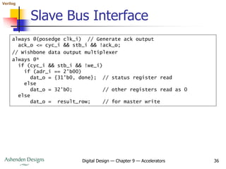
![Verilog
Digital Design — Chapter 9 — Accelerators 35
Slave Bus Interface
assign start = cyc_i && stb_i && we_i && adr_i == 2'b01;
assign O_base_ce = cyc_i && stb_i && we_i && adr_i == 2'b10;
assign D_base_ce = cyc_i && stb_i && we_i && adr_i == 2'b11;
always @(posedge clk_i) // Interrupt enable register
if (rst_i)
int_en <= 1'b0;
else if (cyc_i && stb_i && we_i && adr_i == 2'b00)
int_en <= dat_i[0];
always @(posedge clk_i) // Status register
if (rst_i)
done <= 1'b0;
else if (done_set)
// This occurs when last write is acknowledged,
// and so cannot coincide with a read of the status register.
done <= 1'b1;
else if (cyc_i && stb_i && we_i && adr_i == 2'b00 && ack_o)
done <= 1'b0;
assign int_req = int_en && done;
...](https://image.slidesharecdn.com/09accelerators-210924153936/85/09-accelerators-35-320.jpg)
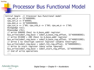
![Verilog
Digital Design — Chapter 9 — Accelerators 42
Processor Bus Functional Model
cpu_cyc_o = 1'b0; cpu_stb_o = 1'b0; cpu_we_o = 1'b0;
begin: loop
forever begin
#10000;
@(posedge clk);
// Read status register
cpu_adr_o <= sobel_reg_base + sobel_status_reg_offset;
cpu_sel_o <= 4'b1111;
cpu_cyc_o <= 1'b1; cpu_stb_o <= 1'b1; cpu_we_o <= 1'b0;
@(posedge clk); while (!cpu_ack_i) @(posedge clk);
cpu_cyc_o <= 1'b0; cpu_stb_o <= 1'b0; cpu_we_o <= 1'b0;
if (cpu_dat_i[0]) disable loop;
end
end
end](https://image.slidesharecdn.com/09accelerators-210924153936/85/09-accelerators-42-320.jpg)