Water-splitting photoelectrodes consisting of heterojunctions of carbon nitride with a p-type low bandgap double perovskite oxide
•Download as PPTX, PDF•
0 likes•73 views

This document describes the synthesis and characterization of a nanocomposite material consisting of graphitic carbon nitride (g-C3N4 or CN) and the double perovskite oxide Ba2Ca0.66Nb0.68Fe0.33Co0.33O6-δ (BCNFCo) for use as a photocatalyst in water splitting applications. The nanocomposite, BCNFCo/CN, is formed by a solvothermal method and exhibits a heterojunction between the p-type BCNFCo and n-type CN. Characterization using techniques such as TEM, XRD, UV-Vis spectroscopy, and photocurrent measurements show the materials have suitable

Recommended
Recommended
More Related Content
What's hot
What's hot (20)
Similar to Water-splitting photoelectrodes consisting of heterojunctions of carbon nitride with a p-type low bandgap double perovskite oxide
Similar to Water-splitting photoelectrodes consisting of heterojunctions of carbon nitride with a p-type low bandgap double perovskite oxide (20)
More from Pawan Kumar
More from Pawan Kumar (20)
Recently uploaded
Recently uploaded (20)
Water-splitting photoelectrodes consisting of heterojunctions of carbon nitride with a p-type low bandgap double perovskite oxide
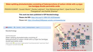
- 1. Water-splitting photoelectrodes consisting of heterojunctions of carbon nitride with a p-type low bandgap double perovskite oxide PAWAN KUMAR1, Suresh Mulmi2, Devika Laishram3, Kazi Mohammad Alam4, Ujwal Kumar Thakur4, V Thangadurai5 and Karthik Shankar4 This work has been published in IOP Nanotechnology Please cite DOI: https://doi.org/10.1088/1361-6528/abedec Please visit: https://choudhary2486pawan.wixsite.com/pawankumar
- 2. Fig. 1. Synthesis protocol for formation of Ba2Ca0.66Nb0.68Fe0.33Co0.33O6-δ/g-C3N4 (BCNFCo/CN) nanocomposite.
- 3. Fig. 2. TEM images of CN (a) Low magnification image at 0.5 µm scale bar and (b) Moderate magnification image at 100 nm scale bar showing nanosheets structure (c) HR-TEM image at 10 nm scale bar showing nanoporous structure; inset showing corresponding FFT image (d) HR-TEM of BCNFCo/CN nanohybrid at 5 nm scale bar 50 nm scale bar showing wrapped CN over BCNFCo. (e) HR-TEM images of BCNFCo/CN at 5 nm scale bar demonstrating BCNFCo entrapped in CN matrix, Inset 1 and 2 are FFT of selected region showing amorphous CN and crystalline BCNFCo domains (f) Enlarged region showing close contact between CN and BCNFCo and iFFT showing lattice fringes overlapping with crystal plane of BCNFCo and corresponding d-spacing (g) High magnification image at 5 nm scale bar showing lattice fringes of double perovskite oxide and wrapping of CN around the lattice; inset FFT of entire images and (f) Magnified view of the selected area showing interplanar d-spacing and corresponding iFFT overlapped showing 0.27 nm d-spacing.
- 4. Fig. 3. STEM EDX elemental mapping of 40% BCNFCo/CN nanocomposite (a) Bright field (BF) image of mapped area, and EDX elemental mapping for (b) Ba (red), (c) Ca (blue), (d) Co (green), (e) Fe (cyan), (f) Nb (magenta), (g) O (pink), (h) C (yellow), (i) N (violet); (j) Composite image for Ba, Ca, Co, Fe, Nb, O (k) composite of C, N and (l) Composite of Ba, Ca, Co, Fe, Nb, O, C and N.
- 5. Fig. 4. (a) FTIR spectra of BCNFCo, CN and 40% BCNFCo/CN, (b) Raman spectra of BCNFCo, CN and 40% BCNFCo/CN (c) Powder XRD (P-XRD) diffraction pattern of CN, BCNFCo and their composites with different wt%; Color: CN (black), 10% BCNFCo/CN (pink), 20% BCNFCo/CN (green), 30% BCNFCo/CN (blue), 40% BCNFCo/CN (red), 50% BCNFCo/CN (yellow), BCNFCo (violet).
- 6. Fig. 5. (a) DR-UV-Vis spectra and (b) Steady-state PL (ssPL) spectra of CN, 10% BCNFCo/CN, 20% BCNFCo/CN, 30% BCNFCo/CN, 40% BCNFCo/CN, 50% BCNFCo/CN, BCNFCo acquired at 360 nm excitation; Color: CN (black), 10% BCNFCo/CN (pink), 20% BCNFCo/CN (green), 30% BCNFCo/CN (blue), 40% BCNFCo/CN (red), 50% BCNFCo/CN (yellow), BCNFCo (violet).
- 7. Fig. 6. (a) Linear sweep voltammograms of CN, 10% BCNFCo/CN, 20% BCNFCo/CN, 30% BCNFCo/CN, 40% BCNFCo/CN, 50% BCNFCo/CN, BCNFCo samples showing change in photocurrent density vs applied potential (J-V), under dark and simulated solar AM1.5G light irradiation (100 mW cm−2) (b) Photocurrent vs time (i-t) plot showing response during light On-Off cycles at +0.6 V applied bias, under AM1.5G light irradiation (100 mW cm−2); All the measurements were performed in 0.1 M Na2SO4 solution at a scan rate of 0.1 mV/sec and (c) Calculated Faradaic efficiencies for hydrogen evolution using BCNFCo, CN and 40% BCNFCo/CN photocatalyst.
- 8. Fig. 7. (a) Linear sweep voltammogram of 40% BCNFCo/CN showing photocurrent density vs applied potential (J-V), photoresponse during light On-Off cycle under dark, solar simulated AM1.5G light irradiation without filter (100 mW cm−2) and AM1.5G light irradiation with 420 nm cut-off filter, (b) Photocurrent vs time (i-t) plot of 40% BCNFCo/CN showing response during light On-Off cycle at +0.6 V applied bias, under solar simulated AM1.5G light irradiation without filter (100 mW cm−2) and AM1.5G light irradiation with 420 nm cut-off filter, (c) Photocurrent response vs time of 40% BCNFCo/CN during the light On-Off cycle at +0.6 V applied bias, under 420, 460, 520, 580, 640 and 840 nm LEDs (100 mW cm−2) (d) Enlarged photocurrent vs time graph showing photoresponse of 40% BCNFCo/CN under 580, 640 and 840 nm LEDs (100 mW cm−2) All the measurement were performed in 0.1 M Na2SO4 solution at a scan rate of 0.1 mV/sec.
- 9. Fig. 8. XPS valence band (XPS-VB) spectra showing valence band position with respect to Fermi level of (a) CN, (b) BCNFCo and (c) 40% BCNFCo/CN and Mott-Schottky plots showing flat and potential of CN (black), 10% BCNFCo/CN (pink), 20% BCNFCo/CN (green), 30% BCNFCo/CN (blue), 40% BCNFCo/CN (red), 50% BCNFCo/CN (yellow).
- 10. Fig. 9. A plausible mechanism of Fermi level alignment and formation of p-n heterojunction between BCNFCo and CN.
- 11. Figure S1. Inner shell ionization edge (core loss) electron energy loss spectra (EELS) of graphitic carbon nitride (CN) showing contribution of σ* and π* signals in C K-edge and N K-edge energy loss.
- 12. Figure S2. STEM EDX elemental mapping of 40% BCNFCo/CN nanocomposite (a) bright field (BF) image of mapped area and EDX elemental mapping for (b) Ba (red), (c) Ca (blue), (d) Co (green), (e) Fe (cyan), (f) Nb (magenta), (g) O (pink), (h) C (yellow), (i) N (violet), (j) composite image for Ba, Ca, Co, Fe, Nb, O (k) composite of C, N, (l) composite of Fe, Co and Nb (m) composite of Co, Fe, C and N (n) composite of Ba, Nb and N (o) composite of Ba, Ca, Co, Fe, Nb, O, C and N.
- 13. Figure S3. (a) RGB composite of EDX elemental mapping for Ba (red), C (green), N (blue) (b) Line scan of RGB composite showing the relative distribution of each elements, (c) RGB composite of EDX elemental mapping for Ca (red), C (green), N (blue) (b) Line scan of RGB composite showing the relative distribution of each elements
- 14. Figure S4. (a) XPS elemental survey scan of CN, and HR-XPS spectra of CN in (b) C1s, (c) N1s, and (d) O1s regions.
- 15. Figure S5. (a) XPS elemental survey scan of BCNFCo, and HR-XPS spectra of BCNFCo in (b) Ba3d, (c) Ca2p, (d) Nb3d, (e) Fe2p, (f) O1s region
- 16. Figure S6. (a) XPS elemental survey scan of 40% BCNFCo/CN composite, and HR-XPS spectra of 40% BCNFCo/CN in (b) C1s, (c) N1s, (d) Ba3d, (e) Ca2p, (f) Nb3d, (g) Fe2p, (h) O1s region.
- 17. Figure S7. (a) Tauc plot of CN (black), 10% BCNFCo/CN (pink), 20% BCNFCo/CN (green), 30% BCNFCo/CN (blue), 40% BCNFCo/CN (red), 50% BCNFCo/CN (yellow), BCNFCo (violet).
- 18. Figure S8. An idealized crystal structure of cubic double-perovskite Ba3CaNb2O9.
- 19. Figure S9. Powder X-ray diffraction (PXRD) Rietveld refinement plot of double-perovskite- type Ba2Ca0.67Nb0.67Fe0.33Co0.33O6-δ using Fm-3m (No. 225) space group.
- 20. Figure S10. TGA thermogram of CN (blue) and 40% BCNFCo/CN catalyst
- 21. Figure S11. GC chromatogram of the cathodic gaseous product on Pt counter electrode, showing peaks for evolved H2 in PEC water splitting using BCNFCo, CN and 40% BCNFCo/CN photocatalyst under AM1.5 irradiation (100 mW cm-2).
- 22. Figure S12. Experimental (points) and fitted (line) EIS Nyquist plots of (a) CN (black), 10% BCNFCo/CN (pink), 20% BCNFCo/CN (green), 30% BCNFCo/CN (blue), 40% BCNFCo/CN (red), 50% BCNFCo/CN (yellow), BCNFCo (violet) under dark and (b) CN (black), 10% BCNFCo/CN (red), 20% BCNFCo/CN (magenta), 30% BCNFCo/CN (navy blue), 40% BCNFCo/CN (violet), 50% BCNFCo/CN (yellow), BCNFCo (blue) under AM1.5 G solar simulated light (100 mW cm-2). Insets shows Equivalent circuit of EIS data under dark and illumination conditions respectively.
- 23. Figure S13. (a) Linear sweep voltammogram of CN showing photocurrent density vs applied potential (J-V), photoresponse during light On-Off cycle under dark, solar simulated AM1.5G light irradiation without filter (100 mW cm−2) and AM1.5G light irradiation with 420 nm cut-off filter, (b) Photocurrent vs time (i-t) plot of CN showing response during the light On-Off cycle at +0.6 V applied bias, under solar simulated AM1.5G light irradiation without filter (100 mW cm−2) and AM1.5G light irradiation with 420 nm cut-off filter, (c) Photocurrent response vs time of CN during the light On-Off cycle at +0.6 V applied bias, under 420, 460, 520, 580, 640, 740 and 840 nm LEDs (100 mW cm−2) (d) Enlarged photocurrent vs time graph showing photoresponse of CN under 580, 640, 740 and 840 nm LEDs (100 mW cm−2) All the measurement were performed in 0.1 M Na2SO4 solution at a scan rate of 0.1 mV/sec.
- 24. Figure S14. (a) Linear sweep voltammogram of BCNFCo showing photocurrent density vs applied potential (J-V), photoresponse during light On-Off cycle under dark, solar simulated AM1.5G light irradiation without filter (100 mW cm−2) and AM1.5G light irradiation with 420 nm cut-off filter, (b) Photocurrent vs time (i-t) plot of BCNFCo showing response during the light On-Off cycle at +0.6 V applied bias, under solar simulated AM1.5G light irradiation without filter (100 mW cm−2) and AM1.5G light irradiation with 420 nm cut-off filter, (c) Photocurrent response vs time of BCNFCo during the light On-Off cycle at +0.6 V applied bias, under 420, 460, 520, 580, 640 and 840 nm LEDs (100 mW cm−2) (d) Enlarged photocurrent vs time graph showing photoresponse of BCNFCo under 580, 640 and 840 nm LEDs (100 mW cm−2) All the measurement were performed in 0.1 M Na2SO4 solution at a scan rate of 0.1 mV/sec.
- 25. Figure S15. (a) Linear sweep voltammogram of 10% BCNFCo/CN showing photocurrent density vs applied potential (J-V), photoresponse during light On-Off cycle under dark, solar simulated AM1.5G light irradiation without filter (100 mW cm−2) and AM1.5G light irradiation with 420 nm cut-off filter, (b) Photocurrent vs time (i-t) plot of 10% BCNFCo/CN showing response during light On-Off cycle at +0.6 V applied bias, under solar simulated AM1.5G light irradiation without filter (100 mW cm−2) and AM1.5G light irradiation with 420 nm cut-off filter, (c) Photocurrent response vs time of 10% BCNFCo/CN during the light On-Off cycle at +0.6 V applied bias, under 420, 460, 520, 580, 640 and 840 nm LEDs (100 mW cm−2) (d) Enlarged photocurrent vs time graph showing photoresponse of 10% BCNFCo/CN under 580, 640 and 840 nm LEDs (100 mW cm−2) All the measurement were performed in 0.1 M Na2SO4 solution at a scan rate of 0.1 mV/sec.
- 26. Figure S16. (a) Linear sweep voltammogram of 20% BCNFCo/CN showing photocurrent density vs applied potential (J-V), photoresponse during light On-Off cycle under dark, solar simulated AM1.5G light irradiation without filter (100 mW cm−2) and AM1.5G light irradiation with 420 nm cut-off filter, (b) Photocurrent vs time (i-t) plot of 20% BCNFCo/CN showing response during light On-Off cycle at +0.6 V applied bias, under solar simulated AM1.5G light irradiation without filter (100 mW cm−2) and AM1.5G light irradiation with 420 nm cut-off filter, (c) Photocurrent response vs time of 20% BCNFCo/CN during the light On-Off cycle at +0.6 V applied bias, under 420, 460, 520, 580, 640 and 840 nm LEDs (100 mW cm−2) (d) Enlarged photocurrent vs time graph showing photoresponse of 20% BCNFCo/CN under 580, 640 and 840 nm LEDs (100 mW cm−2) All the measurement were performed in 0.1 M Na2SO4 solution at a scan rate of 0.1 mV/sec.
- 27. Figure S17. (a) Linear sweep voltammogram of 30% BCNFCo/CN showing photocurrent density vs applied potential (J-V), photoresponse during light On-Off cycle under dark, solar simulated AM1.5G light irradiation without filter (100 mW cm−2) and AM1.5G light irradiation with 420 nm cut-off filter, (b) Photocurrent vs time (i-t) plot of 30% BCNFCo/CN showing response during light On-Off cycle at +0.6 V applied bias, under solar simulated AM1.5G light irradiation without filter (100 mW cm−2) and AM1.5G light irradiation with 420 nm cut-off filter, (c) Photocurrent response vs time of 30% BCNFCo/CN during the light On-Off cycle at +0.6 V applied bias, under 420, 460, 520, 580, 640 and 840 nm LEDs (100 mW cm−2) (d) Enlarged photocurrent vs time graph showing photoresponse of 30% BCNFCo/CN under 580, 640 and 840 nm LEDs (100 mW cm−2) All the measurement were performed in 0.1 M Na2SO4 solution at a scan rate of 0.1 mV/sec.
- 28. Figure S18. (a) Linear sweep voltammogram of 50% BCNFCo/CN showing photocurrent density vs applied potential (J-V), photoresponse during light On-Off cycle under dark, solar simulated AM1.5G light irradiation without filter (100 mW cm−2) and AM1.5G light irradiation with 420 nm cut-off filter, (b) Photocurrent vs time (i-t) plot of 50% BCNFCo/CN showing response during light On-Off cycle at +0.6 V applied bias, under solar simulated AM1.5G light irradiation without filter (100 mW cm−2) and AM1.5G light irradiation with 420 nm cut-off filter, (c) Photocurrent response vs time of 50% BCNFCo/CN during the light On-Off cycle at +0.6 V applied bias, under 420, 460, 520, 580, 640 and 840 nm LEDs (100 mW cm−2) (d) Enlarged photocurrent vs time graph showing photoresponse of 50% BCNFCo/CN under 580, 640 and 840 nm LEDs (100 mW cm−2) All the measurement were performed in 0.1 M Na2SO4 solution at a scan rate of 0.1 mV/sec.