Consistently high Voc values in p-i-n type perovskite solar cells using Ni3+-doped NiO nanomesh as the hole transporting layer

Leading edge p-i-n type halide perovskite solar cells (PSCs) severely underperform n-i-p PSCs. p-i-n type PSCs that use PEDOT:PSS HTLs struggle to generate open circuit photovoltage (Voc) values higher than 1 V. NiO HTLs have shown greater promise in achieving high Voc values albeit inconsistently. In this report, a NiO nanomesh with Ni3+ defect grown by the hydrothermal method was used to obtain PSCs with Voc values that consistently exceeded 1.10 V (champion Voc = 1.14 V). A champion device photoconversion efficiency (PCE) of 17.75% was observed. Density functional theory (DFT) modeling was used to understand the interfacial properties of the NiO/perovskite interface. The PCE of PSCs constructed using the Ni3+-doped NiO nanomesh HTL was ~34% higher than that of conventional compact NiO based perovskite solar cells. A suite of characterization techniques such as transmission electron microscopy (TEM), field emission scanning electron microscopy (FE-SEM), intensity-modulated photocurrent spectroscopy (IMPS), intensity-modulated photovoltage spectroscopy (IMVS), time-resolved photoluminescence (TRPL), steady-state photoluminescence (PL), and Kelvin probe force microscopy (KPFM) provided evidence of better film quality, enhanced charge transfer and suppressed charge recombination in PSCs based on hydrothermally grown NiO nanostructures.

Recommended
Recommended
More Related Content
Similar to Consistently high Voc values in p-i-n type perovskite solar cells using Ni3+-doped NiO nanomesh as the hole transporting layer
Similar to Consistently high Voc values in p-i-n type perovskite solar cells using Ni3+-doped NiO nanomesh as the hole transporting layer (20)
More from Pawan Kumar
More from Pawan Kumar (20)
Recently uploaded
Recently uploaded (20)
Consistently high Voc values in p-i-n type perovskite solar cells using Ni3+-doped NiO nanomesh as the hole transporting layer
- 1. Consistently high Voc values in p-i-n type perovskite solar cells using Ni3+-doped NiO nanomesh as the hole transporting layer https://doi.org/10.1021/acsami.9b18197 ACS Applied Materials and Interfaces
- 2. Figure 1. Optimized structures showing the HOMO (left) and LUMO (right) orbitals for three mutual orientations of an NiO (lower) – perovskite (upper) interfacial region. These geometries are referred to as G1, G2, and G3. The upper row shows the MAPbI3 and the lower row represents the MAPbBr3 perovskite nanoparticles. In the NiO structure, nickel atoms are represented by green spheres and oxygen atoms are represented by red ones. In the perovskite structure, the brown and pink spheres represent Br and I, respectively, dark gray ones represent Pb atoms, and the other colors indicate the atomic components of MA groups.
- 3. Figure 2. Schematic diagram illustrating the NiO nanostructure synthesis procedure (top row) and perovskite solar cell (bottom row) fabrication methods.
- 4. Figure 3. Top-view FE-SEM images of NiO (a, b) compact film and a device cross-section (c), a NiO nanostructured layer fabricated with 1 mM, of NiCl2.6H2O in the growth solution (d, e) and the device cross-section (f). Top-view FE-SEM image of nanostructured NiO deposited over FTO substrate used for EDX mapping (g), and mapping for Ni (h), Sn (i) and O (k). Cross-sectional FESEM image of nanostructured NiO based solar cell used for the EDX mapping (k), and mapping for Sn (l), Ni (m), Pb (n), I (o), Br (p), Zn (q) and overlaid image (r). Editor-02
- 5. Figure 4. HRTEM image showing cross-sectional view of (a) nanostructured NiO (1 mM NiCl2.6H2O) and (b) compact NiO thin films showing the thickness and morphology of NiO deposited on the FTO (note: the less dense layer above NiO is carbon film coated on the sample to prevent samples charging during FIB treatment; (c) and (d) high-resolution TEM images of nanostructured and compact NiO films showing lattice fringe contrast. The inset shows a 0.24 nm interplaner spacing consistent with the (111) planes of NiO.
- 6. Figure 5. Core level HR-XPS spectra of NiO nanostructure fabricated with 1 mM, of NiCl2- .6H2O in (a) Ni2p region (b) O1s region.
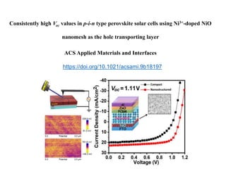
- 7. Figure 6. (a) Current-voltage curves of perovskite solar cells made with compact and nanostructured NiO hole transporting layers. The measurement was carried out under AM1.5 G illumination at 100 mW/cm2 with an active area of 5 mm2. (b) Normalized IPCE spectra of perovskite solar cells made with different NiO hole transporting layers.
- 8. Table 1. Photovoltaic performance summary of perovskite solar cells made with compact and nanostructured NiO, the latter with different concentration of NiCl2.6H2O in the growth solution.
- 9. Figure 7. UPS work function spectra of the (a) thin film compact NiO, (b) nanostructured NiO. Insets show the calculation of cut-off energy (Ecut-off) of the secondary electron and the UPS valance band spectra showing valance band maxima position below Fermi level for (c) thin film compact NiO, (d) nanostructured NiO.
- 10. Figure 8. (a) Photovoltage as a function of intensity of 633 nm LED (b), Nyquist plot of intensity-modulated photovoltage spectroscopy (IMVS), (c) Imaginary part of IMVS as a function of frequency (d) and Mott-Schottky plot of the perovskite solar cells based on compact and nanostructured NiO hole transporting layer.
- 11. Figure 9. (a) Steady-state PL spectra, (b) Time-resolved photoluminescence spectra, (c) Nyquist plot of IMPS spectra, and (d) Imaginary part of IMPS as a function of the frequency of the perovskite solar cells based on compact and nanostructured NiO hole transporting layers.
- 12. Figure 10. (a) Schematic illustration of the KPFM measurement setup, (b) CPD distribution in dark and under illumination for compact NiO based sample (c) CPD distribution in dark and under illumination for nanostructured NiO based sample. The topography AFM image of perovskite layer deposited over (d) compact NiO and (g) NiO nanostructure. Surface potential map measured in the dark of perovskite layer deposited over (e) compact NiO and (h) NiO nanostructure. Surface potential map measured under the illumination of perovskite layer deposited over (f) compact NiO and (i) NiO nanostructure.
- 13. Figure S1: Density of state distribution for NiO surface and (a) MAPbI3 cluster and (b) MAPbBr3 cluster.
- 14. Figure S2: Top SEM image of NiO nanostructure made with 0.5 mM concentration of NiCl2.6H2O in growth solution showing exposed FTO substrate.
- 15. Figure S3: Tilted cross-sectional SEM image of NiO nanostructure made with a 1.0 mM concentration of NiCl2.6H2O in growth solution shows conformal deposition of NiO on FTO substrate.
- 16. Figure S4: Top-view FESEM images of NiO nanostructure (a, b) made with 3 mM and (d,e) 5 mM of NiCl2.6H2O. Cross-sectional image of perovskite solar cell made with (c) 3mM and (f) 5mM of NiCl2.6H2O.
- 17. Figure S5: HR-TEM image of nanostructure NiO film (1 mM NiCl2.6H2O) (a) side view of FIB snipped sample, (b) and (c) high magnification TEM images at 5 nm scale bar showing lattice fringes, and (d) SAED pattern showing diffraction rings.
- 18. Figure S6: HR-TEM image of compact NiO thin film (a) side view of FIB snipped sample, (b) and (c) high magnification TEM images at 5 nm scale bar and (d) TEM image showing FTO and NiO interfacial contact.
- 19. Figure S7: (a) XRD spectra and (b) Raman spectra of compact NiO and NiO nanostructures prepared with different concertation of NiCl2.6H2O in hydrothermal growth solution.
- 20. Figure S8: UV-vis absorption spectra of (a) SQ2 dissolved in 0.1 M KOH, (b), FTO deposited nanostructured NiO and (c) compact NiO, monolayer SQ2 deposited over (d) nanostructured NiO and (e) compact NiO, KOH assisted desorbed SQ2 from (f) nanostructured and (g) compact NiO.
- 21. Figure S9: Tauc plots of NiO nanostructures made with different concentration of NiCl2.6H2O in growth solution.
- 22. Figure S10: XPS elemental survey scan of NiO network thin film.
- 23. Figure S11: Current-voltage curves of perovskite solar cell made with PEDOT: PSS as hole transporting layer. The measurement was carried out under AM1.5 G illumination at 100 mW/cm2 with an active area of 6 mm2.
- 24. Figure S12: Box charts of (a) Voc, (b) JSC, (c) FF and (d) PCE for perovskite solar cells based on compact NiO and NiO nanostructure made with different concentration of NiCl2.6H2O.
- 25. Figure S13: Current-voltage curves of perovskite solar cell made with nanostructure NiO hole transporting layer made with 3 mM and 5 mM of NiCl2.6H2O. The measurement was carried out under AM1.5 G illumination at 100 mW/cm2 with an active area of 6 mm2.
- 26. A1 τ1 A2 τ2 A3 τ3 τavg Bare FTO 0.43 11.92 0.39 151.37 - - 54.73 FTO/Compact NiO 0.89 1.71 0.13 13.19 0.041 569.89 20.17 FTO/NiO nanostructure 0.85 1.55 0.19 8.37 0.013 122.25 1.51 Table S3: Fitting parameters of time resolved photoluminescence spectra for HTL free perovskite layer and perovskite layer deposited over compact and nanostructured NiO coated FTO substrate. The values of the goodness-of-fit parameter (r2) are all close to 1.0