
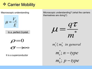
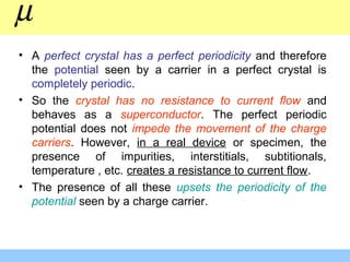
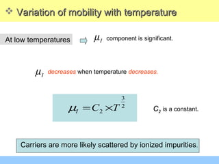
![ Carrier Mobility ,Carrier Mobility , µ
dV Eµ=
:E
:µ
applied field
mobility of charge carrier
[ ]
−
=
SecV
cm
2
µ µ is a proportionality factor
=
E
Vd
µ
So is a measure how easily charge carriers move under the influence of
an applied field or determines how mobile the charge carriers are.
µ
µ](https://image.slidesharecdn.com/mobility-140821022335-phpapp01/85/Mobility-5-320.jpg)
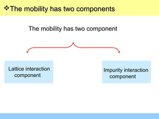
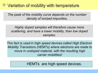
![ A Derivation of Ohm’s LawA Derivation of Ohm’s Law
2
2
1
d d d
d
d
x d x x
x x
I nqV A V E
I q
J
A m
nq
J nqV nq E J E
m
nq
J E
m
µ
τ
µ
τ
µ
τ
σ σ ρ
σ
∗
∗
∗
= =
= =
= = = ÷
= = =
[ ] [ ]
[ ] [ ]1 ( )
m
m
ρ
σ
= Ω−
= Ω−](https://image.slidesharecdn.com/mobility-140821022335-phpapp01/85/Mobility-23-320.jpg)
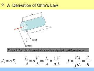
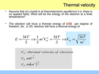
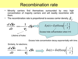
![ FluxFlux
[ ]
[ ]
2 1
2
2
,
,th
n n n
p p p
n p
Flux m s
D l D m s
The current densities for electrons and holes
dn dn
J q D qD for electrons
dx dx
dp dp
J q D qD for holes
dx dx
J A m
ν
− −
= −
= =
= − − = ÷
= + − = − ÷
= ](https://image.slidesharecdn.com/mobility-140821022335-phpapp01/85/Mobility-37-320.jpg)
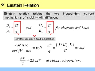

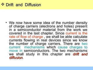
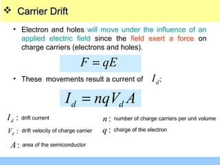
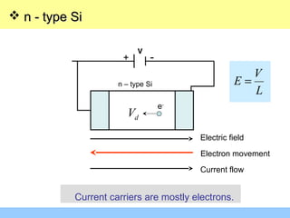
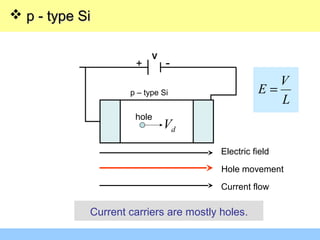
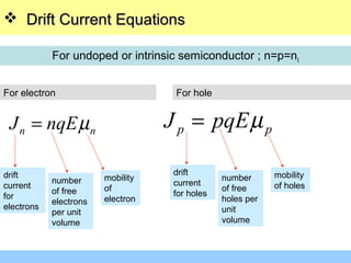
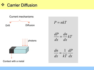
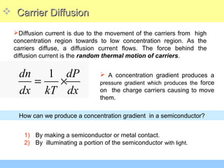
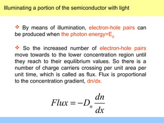
The document discusses various mechanisms of charge carrier transport in semiconductors including drift and diffusion. It defines carrier drift as the movement of electrons and holes under the influence of an applied electric field. Carrier mobility is introduced as a material property that determines how fast carriers drift in response to an electric field. Diffusion is defined as the movement of carriers from areas of high concentration to low concentration due to random thermal motion. The Einstein relation links diffusion and mobility through the carrier temperature. Total current in a semiconductor is the sum of drift and diffusion currents.