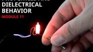
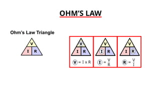
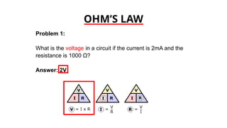
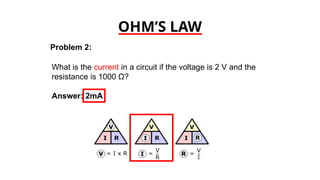
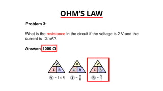
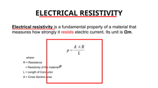
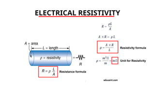
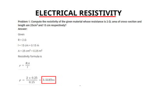
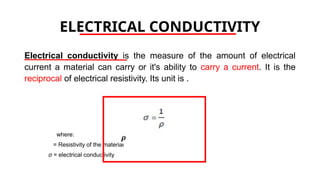
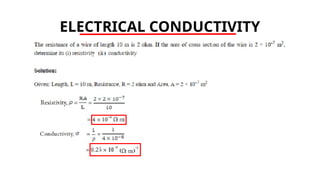
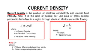
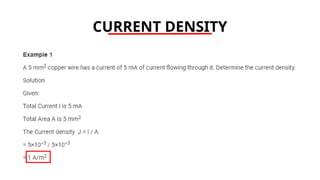
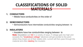
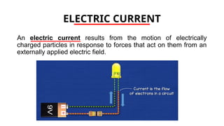
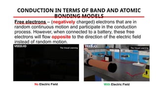
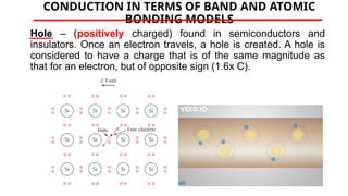
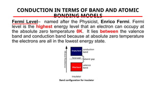
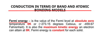
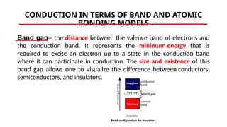
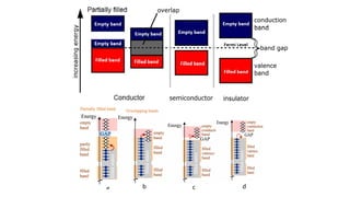
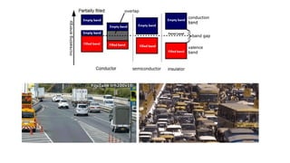
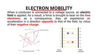
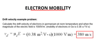
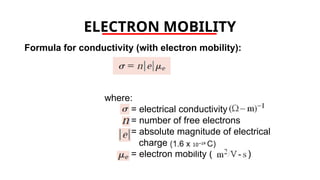
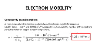
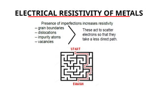
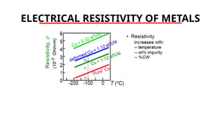
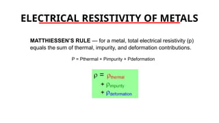
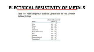
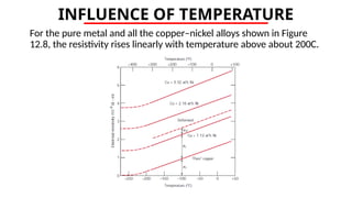
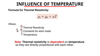
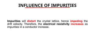
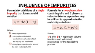
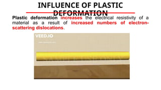
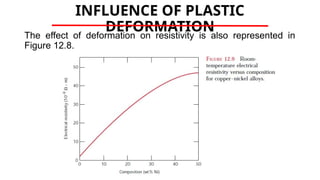
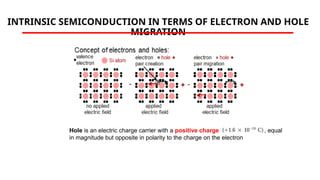
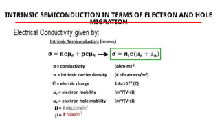
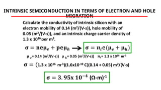
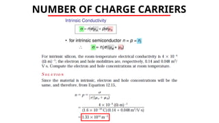
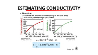
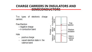
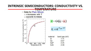
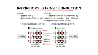
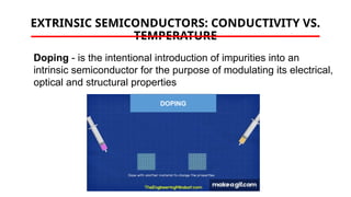
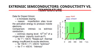
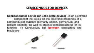
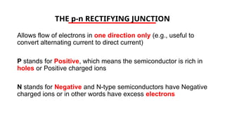
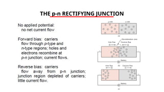
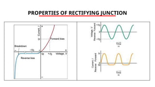
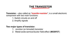
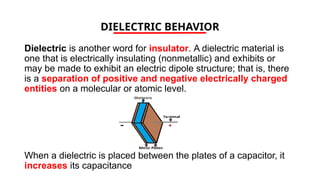
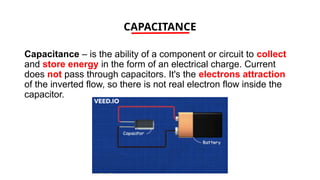
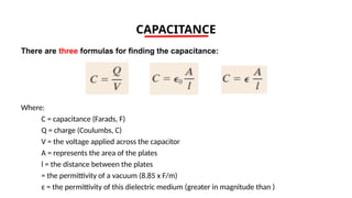
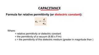
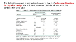
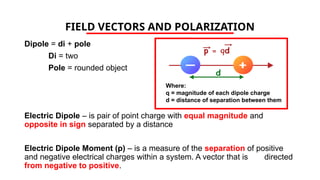
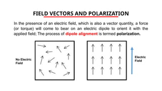
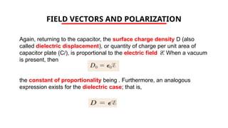
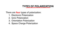
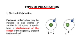
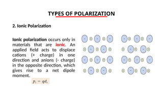
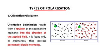
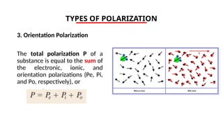
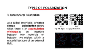
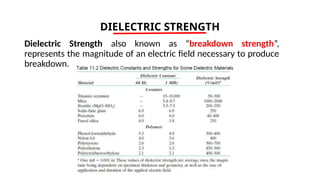
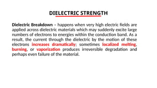
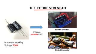
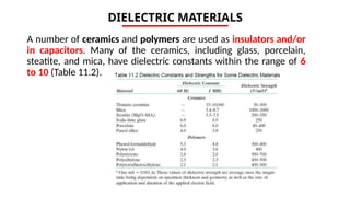
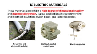
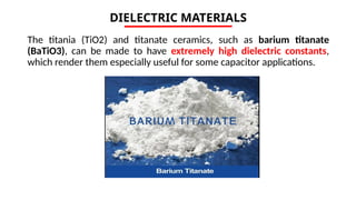
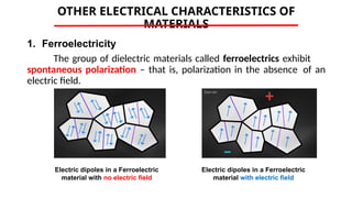
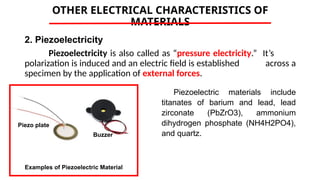
GROUP INFORMATION
GROUP: 7
TOPIC: ELECTRICAL PROPERTIES AND DIELECTRICAL BEHAVIOR
MEMBERS:
• Elevado, Edgar Jr. M. (1st
Presentor)
• Espinosa, Joemary C. (2nd
Presentor)
• Florendo, Justin (3rd
Presentor)
• Ganal, Ceejay (4th
Presentor)
• Jervoso, Frence Jarvy (5th
Presentor)
PROPERTIES AND
DIELECTRICAL
BEHAVIOR
MODULE 11
OHM’S LAW
Georg Simon Ohm – German physicist who
discovered the law, named after him, which
states that the current flow through a conductor is
directly proportional to the voltage and inversely
proportional to the resistance
V=IR
where:
V = Voltage (V)
I = Current (A)
R = Resistance (Ω)
OHM’S LAW
OHM’S LAW
Ohm’s Law Triangle
OHM’S LAW
Problem 1:
What is the voltage in a circuit if the current is 2mA and the
resistance is 1000 Ω?
Answer: 2V
OHM’S LAW
Problem 2:
What is the current in a circuit if the voltage is 2 V and the
resistance is 1000 Ω?
Answer: 2mA
OHM’S LAW
Problem 3:
What is the resistance in the circuit if the voltage is 2 V and the
current is 2mA?
Answer: 1000 Ω
ELECTRICAL RESISTIVITY
Electrical resistivity is a fundamental property of a material that
measures how strongly it resists electric current. Its unit is Ωm.
where:
R = Resistance
= Resistivity of the material
L = Length of Conductor
A = Cross Section Area
ELECTRICAL RESISTIVITY
Resistance formula
Unit for Resistivity
Resistivity formula
ELECTRICAL RESISTIVITY
ELECTRICAL CONDUCTIVITY
Electrical conductivity is the measure of the amount of electrical
current a material can carry or it's ability to carry a current. It is the
reciprocal of electrical resistivity. Its unit is .
where:
= Resistivity of the material
σ = electrical conductivity
ELECTRICAL CONDUCTIVITY
Current density is the product of electrical conductivity and electric field
intensity. Also, it is the ratio of current per unit area of cross section
perpendicular to flow in a region through which an electric current is flowing.
where:
J = Current Density
σ = Electrical Conductivity
E = Electric Field Intensity
CURRENT DENSITY
Where:
I = Current
A = Specimen Area
Note: E =
Where:
V = Voltage difference between two points
l = Distance separating the two points
CURRENT DENSITY
CLASSIFICATIONS OF SOLID
MATERIALS
1. CONDUCTORS
• Metals have conductivities on the order of
2. SEMICONDUCTORS
• Semiconductors have intermediate conductivities ranging between to
3. INSULATORS
• Insulators have low conductivities ranging between to
Note: Insulation can fail in a variety of ways, if voltage gets too high and
exceeds the "breakdown voltage" electrons will get excited to the point
where they break out of their stable orbit, current will then pass through the
material and often destroy the insulator.
ELECTRIC CURRENT
An electric current results from the motion of electrically
charged particles in response to forces that act on them from an
externally applied electric field.
ELECTRIC CURRENT
Within most solid materials a current arises from the flow of
electrons, which is termed electronic conduction.
For ionic materials, a net motion of charged ions is possible that
produces a current; such is termed ionic conduction.
CONDUCTION IN TERMS OF BAND AND ATOMIC
BONDING MODELS
Free electrons – (negatively charged) electrons that are in
random continuous motion and participate in the conduction
process. However, when connected to a battery, these free
electrons will flow opposite to the direction of the electric field
instead of random motion.
With Electric Field
No Electric Field
CONDUCTION IN TERMS OF BAND AND ATOMIC
BONDING MODELS
Hole – (positively charged) found in semiconductors and
insulators. Once an electron travels, a hole is created. A hole is
considered to have a charge that is of the same magnitude as
that for an electron, but of opposite sign (1.6x C).
CONDUCTION IN TERMS OF BAND AND ATOMIC
BONDING MODELS
Fermi Level– named after the Physicist, Enrico Fermi. Fermi
level is the highest energy level that an electron can occupy at
the absolute zero temperature 0K. It lies between the valence
band and conduction band because at absolute zero temperature
the electrons are all in the lowest energy state.
CONDUCTION IN TERMS OF BAND AND ATOMIC
BONDING MODELS
Fermi energy – is the value of the Fermi level at absolute zero
temperature 0K or (−273.15 degrees Celsius, or -459.67
Fahrenheit). It is also the maximum kinetic energy an electron
can attain at 0K. Fermi energy is constant for each solid.
CONDUCTION IN TERMS OF BAND AND ATOMIC
BONDING MODELS
Band gap– the distance between the valence band of electrons and
the conduction band. It represents the minimum energy that is
required to excite an electron up to a state in the conduction band
where it can participate in conduction. The size and existence of this
band gap allows one to visualize the difference between conductors,
semiconductors, and insulators.
CONDUCTION IN TERMS OF BAND AND ATOMIC
BONDING MODELS
There are four possible band configurations:
a. Partially Filled Bands (metals/conductors)
b. Overlapping Bands (metals/conductors)
c. Semiconductors
- narrow band gap (< 2 eV) note: eV = electron Volt
- more electrons excited across band gap
d. Insulators
- wide band gap (> 2 eV)
- few electrons excited across band gap
a b c d
ELECTRON MOBILITY
Electron Mobility – characterizes how quickly an electron can
move through a metal or semiconductor when pulled by an
electric field. In other words, it is simply the frequency of
scattering events. It is represented by .
ELECTRON MOBILITY
When a conductor is connected to a voltage source, an electric
field is applied. As a result, a force is brought to bear on the free
electrons; as a consequence, they all experience an
acceleration in a direction opposite to that of the field, by virtue
of their negative charge.
ELECTRON MOBILITY
Free electrons (negative charge) move in opposite direction
of that of the electric field when a conductor is connected to a
voltage source.
ELECTRON MOBILITY
The scattering of the free electrons will depend on the property of a material.
A semiconductor virtually behaves like an insulator at low temperatures.
However, at room temperature, some free electrons cross over to the conduction
band giving little conductivity to the semiconductor
In insulators, free electrons cannot freely move due to very low conductivity.
The scattering phenomenon is manifested as a resistance to the passage of an
electric current.
Several parameters are used to describe the extent of this scattering, these
include the drift velocity and the mobility of an electron.
ELECTRON MOBILITY
Drift velocity - The drift velocity represents the average electron
velocity in the direction of the force imposed by the applied field.
ELECTRON MOBILITY
Drift speed of electrons is less when compared with its speed in
random motion (no electric field).
With Electric Field No Electric Field
ELECTRON MOBILITY
Formula for Drift Velocity:
where:
= drift velocity ( )
= electron mobility ( )
= electric field ( )
ELECTRON MOBILITY
ELECTRON MOBILITY
Formula for conductivity (with electron mobility):
where:
= electrical conductivity
= number of free electrons
= absolute magnitude of electrical
charge
= electron mobility ( )
ELECTRON MOBILITY
ELECTRICAL RESISTIVITY OF METALS
MATTHIESSEN’S RULE — for a metal, total electrical resistivity (p)
equals the sum of thermal, impurity, and deformation contributions.
P = Pthermal + Pimpurity + Pdeformation
ELECTRICAL RESISTIVITY OF METALS
INFLUENCE OF TEMPERATURE
For the pure metal and all the copper–nickel alloys shown in Figure
12.8, the resistivity rises linearly with temperature above about 200C.
INFLUENCE OF TEMPERATURE
Formula for Thermal Resistivity:
Where:
= Thermal Resistivity
& = Constants for each metal
= Temperature
Note: Thermal resistivity is dependent on temperature
so they are directly proportional with each other.
INFLUENCE OF IMPURITIES
Impurities will distort the crystal lattice, hence impeding the
drift velocity. Therefore, the electrical resistivity increases as
impurities in a conductor increase.
INFLUENCE OF IMPURITIES
Formula for additions of a single
impurity that forms a solid
solution:
Where:
= Impurity Resistivity
= composition-independent
constant that is a function of both
the impurity and host metals.
= impurity concentration ci in terms of
the atom fraction (at%/100)
Formula for a two-phase alloy
consisting of α and β phases, a
rule-of-mixtures expression may
be utilized to approximate the
resistivity as follows:
Where:
V’s and ρ’s = represent volume
fractions and individual
resistivities for the respective
phases
INFLUENCE OF PLASTIC
DEFORMATION
Plastic deformation increases the electrical resistivity of a
material as a result of increased numbers of electron-
scattering dislocations.
INFLUENCE OF PLASTIC
DEFORMATION
The effect of deformation on resistivity is also represented in
Figure 12.8.
SEMI CONDUCTIVITY
Electrical conductivity of the semiconducting materials is not as
high as that of the metals.
The electrical properties of these materials are extremely sensitive
to the presence of even minute concentrations of impurities.
SEMI CONDUCTIVITY
Two types of semiconductors:
1. Intrinsic Semiconductors
• are those in which the electrical behavior is based on the
electronic structure inherent in the pure material.
2. Extrinsic Semiconductors
• Electrical characteristics are dictated by impurity atoms
INTRINSIC SEMICONDUCTORS
INTRINSIC SEMICONDUCTION IN TERMS OF ELECTRON AND HOLE
MIGRATION
Hole is an electric charge carrier with a positive charge , equal
in magnitude but opposite in polarity to the charge on the electron
INTRINSIC SEMICONDUCTION IN TERMS OF ELECTRON AND HOLE
MIGRATION
INTRINSIC SEMICONDUCTION IN TERMS OF ELECTRON AND HOLE
MIGRATION
e e e
NUMBER OF CHARGE CARRIERS
ESTIMATING CONDUCTIVITY
CHARGE CARRIERS IN INSULATORS AND
SEMICONDUCTORS
INTRINSIC SEMICONDUCTORS: CONDUCTIVITY VS.
TEMPERATURE
INTRINSIC VS. EXTRINSIC CONDUCTION
EXTRINSIC SEMICONDUCTORS: CONDUCTIVITY VS.
TEMPERATURE
DOPING
Doping - is the intentional introduction of impurities into an
intrinsic semiconductor for the purpose of modulating its electrical,
optical and structural properties
EXTRINSIC SEMICONDUCTORS: CONDUCTIVITY VS.
TEMPERATURE
SEMICONDUCTOR DEVICES
Semiconductor device (or Solid-state device) - is an electronic
component that relies on the electronic properties of a
semiconductor material (primarily silicon, germanium, and
gallium arsenide, as well as organic semiconductors) for its
function. It's Conductivity lies between conductors and
Insulators
Diodes Transistors
SEMICONDUCTOR DEVICES
Advantages of semiconductor devices:
• small size,
• low power consumption, and
• no warmup time
THE p-n RECTIFYING JUNCTION
Allows flow of electrons in one direction only (e.g., useful to
convert alternating current to direct current)
P stands for Positive, which means the semiconductor is rich in
holes or Positive charged ions
N stands for Negative and N-type semiconductors have Negative
charged ions or in other words have excess electrons
THE p-n RECTIFYING JUNCTION
PROPERTIES OF RECTIFYING JUNCTION
THE TRANSISTOR
Transistor – also called as “transfer-resistor”, is a small electronic
component with two main functions:
1. Switch circuits on and off
2. Amplify signals
Two major types of transistor:
1. Junction (or bimodal) transistor
2. Metal-oxide-semiconductor field-effect (MOSFET)
THE TRANSISTOR
Switch circuits on and off Amplify Signals
DIELECTRIC BEHAVIOR
Dielectric is another word for insulator. A dielectric material is
one that is electrically insulating (nonmetallic) and exhibits or
may be made to exhibit an electric dipole structure; that is, there
is a separation of positive and negative electrically charged
entities on a molecular or atomic level.
When a dielectric is placed between the plates of a capacitor, it
increases its capacitance
CAPACITANCE
Capacitance – is the ability of a component or circuit to collect
and store energy in the form of an electrical charge. Current
does not pass through capacitors. It's the electrons attraction
of the inverted flow, so there is not real electron flow inside the
capacitor.
CAPACITANCE
There are three formulas for finding the capacitance:
Where:
C = capacitance (Farads, F)
Q = charge (Coulumbs, C)
V = the voltage applied across the capacitor
A = represents the area of the plates
l = the distance between the plates
= the permittivity of a vacuum (8.85 x F/m)
ε = the permittivity of this dielectric medium (greater in magnitude than )
CAPACITANCE
Formula for relative permittivity (or dielectric constant):
Where:
= relative permittivity or dielectric constant
= the permittivity of a vacuum (8.85 x F/m)
ε = the permittivity of this dielectric medium (greater in magnitude than )
The dielectric constant is one material property that is of prime consideration
for capacitor design. The values of a number of dielectric materials are
contained in Table 11.2
FIELD VECTORS AND POLARIZATION
Dipole = di + pole
Di = two
Pole = rounded object
Electric Dipole – is pair of point charge with equal magnitude and
opposite in sign separated by a distance
Electric Dipole Moment (p) – is a measure of the separation of positive
and negative electrical charges within a system. A vector that is directed
from negative to positive.
Where:
q = magnitude of each dipole charge
d = distance of separation between them
FIELD VECTORS AND POLARIZATION
In the presence of an electric field, which is also a vector quantity, a force
(or torque) will come to bear on an electric dipole to orient it with the
applied field; The process of dipole alignment is termed polarization.
Electric
Field
No Electric
Field
FIELD VECTORS AND POLARIZATION
Again, returning to the capacitor, the surface charge density D (also
called dielectric displacement), or quantity of charge per unit area of
capacitor plate (C/), is proportional to the electric field E. When a vacuum
is present, then
the constant of proportionality being . Furthermore, an analogous
expression exists for the dielectric case; that is,
TYPES OF POLARIZATION
There are four types of polarization:
1. Electronic Polarization
2. Ionic Polarization
3. Orientation Polarization
4. Space Charge Polarization
TYPES OF POLARIZATION
1. Electronic Polarization
Electronic polarization may be
induced to one degree or
another in all atoms. It results
from a displacement of the
center of the negatively charged
electron cloud
TYPES OF POLARIZATION
2. Ionic Polarization
Ionic polarization occurs only in
materials that are ionic. An
applied field acts to displace
cations (+ charge) in one
direction and anions (- charge)
in the opposite direction, which
gives rise to a net dipole
moment.
TYPES OF POLARIZATION
3. Orientation Polarization
Orientation polarization results
from a rotation of the permanent
moments into the direction of
the applied field. It is found only
in substances that possess
permanent dipole moments.
TYPES OF POLARIZATION
3. Orientation Polarization
The total polarization P of a
substance is equal to the sum of
the electronic, ionic, and
orientation polarizations (Pe, Pi,
and Po, respectively), or
TYPES OF POLARIZATION
4. Space Charge Polarization
Also called ‘Interfacial’ or space
charge polarization occurs
when there is an accumulation
of charge at an interface
between two materials or
between two regions within a
material because of an external
field.
FREQUENCY DEPENDENCE OF THE DIELECTRIC
CONSTANT
Relaxation Frequency – The frequency at which the dielectric loss factor
reaches a maximum, for a dielectric material that has no static (d.c.)
conductivity and that is subjected to an alternating electromagnetic field.
Dielectric Loss – is the absorption of electrical energy by a dielectric
material that is subjected to an alternating electric field.
A low dielectric loss is desired at the frequency of utilization.
FREQUENCY DEPENDENCE OF THE DIELECTRIC
CONSTANT
Silicone rubber is usually a good choice for a buffer
layer due to its very low dielectric loss factor,
high dielectric constant, good mechanical
properties, high dielectric strength, and durability
after many welds.
DIELECTRIC STRENGTH
Dielectric Strength also known as “breakdown strength”,
represents the magnitude of an electric field necessary to produce
breakdown.
DIELECTRIC STRENGTH
Dielectric Breakdown – happens when very high electric fields are
applied across dielectric materials which may suddenly excite large
numbers of electrons to energies within the conduction band. As a
result, the current through the dielectric by the motion of these
electrons increases dramatically; sometimes localized melting,
burning, or vaporization produces irreversible degradation and
perhaps even failure of the material.
DIELECTRIC STRENGTH
If Voltage
exceeds 250V
Maximum Working
Voltage: 250V
Melted Capacitor
Burnt Capacitor
DIELECTRIC MATERIALS
A number of ceramics and polymers are used as insulators and/or
in capacitors. Many of the ceramics, including glass, porcelain,
steatite, and mica, have dielectric constants within the range of 6
to 10 (Table 11.2).
DIELECTRIC MATERIALS
These materials also exhibit a high degree of dimensional stability
and mechanical strength. Typical applications include power line
and electrical insulation, switch bases, and light receptacles.
Power line and
electrical insulation
Lightbulb socket
switch base
Light receptacles
DIELECTRIC MATERIALS
The titania (TiO2) and titanate ceramics, such as barium titanate
(BaTiO3), can be made to have extremely high dielectric constants,
which render them especially useful for some capacitor applications.
DIELECTRIC MATERIALS
The dielectric loss is increased by the following factors:
1. high frequency of the applied voltage
2. high value of the applied voltage
3. high temperature
4. humidity
OTHER ELECTRICAL CHARACTERISTICS OF
MATERIALS
1. Ferroelectricity
The group of dielectric materials called ferroelectrics exhibit
spontaneous polarization – that is, polarization in the absence of an
electric field.
Electric dipoles in a Ferroelectric
material with no electric field
Electric dipoles in a Ferroelectric
material with electric field
OTHER ELECTRICAL CHARACTERISTICS OF
MATERIALS
2. Piezoelectricity
Piezoelectricity is also called as “pressure electricity.” It’s
polarization is induced and an electric field is established across a
specimen by the application of external forces.
Examples of Piezoelectric Material
Piezoelectric materials include
titanates of barium and lead, lead
zirconate (PbZrO3), ammonium
dihydrogen phosphate (NH4H2PO4),
and quartz.
Buzzer
Piezo plate
End of presentation.
Thank you!

Group 7 Report (Module 11 for group 7).pptx

  • 1.
    GROUP INFORMATION GROUP: 7 TOPIC:ELECTRICAL PROPERTIES AND DIELECTRICAL BEHAVIOR MEMBERS: • Elevado, Edgar Jr. M. (1st Presentor) • Espinosa, Joemary C. (2nd Presentor) • Florendo, Justin (3rd Presentor) • Ganal, Ceejay (4th Presentor) • Jervoso, Frence Jarvy (5th Presentor)
  • 2.
  • 3.
    OHM’S LAW Georg SimonOhm – German physicist who discovered the law, named after him, which states that the current flow through a conductor is directly proportional to the voltage and inversely proportional to the resistance V=IR where: V = Voltage (V) I = Current (A) R = Resistance (Ω)
  • 4.
  • 5.
  • 6.
    OHM’S LAW Problem 1: Whatis the voltage in a circuit if the current is 2mA and the resistance is 1000 Ω? Answer: 2V
  • 7.
    OHM’S LAW Problem 2: Whatis the current in a circuit if the voltage is 2 V and the resistance is 1000 Ω? Answer: 2mA
  • 8.
    OHM’S LAW Problem 3: Whatis the resistance in the circuit if the voltage is 2 V and the current is 2mA? Answer: 1000 Ω
  • 9.
    ELECTRICAL RESISTIVITY Electrical resistivityis a fundamental property of a material that measures how strongly it resists electric current. Its unit is Ωm. where: R = Resistance = Resistivity of the material L = Length of Conductor A = Cross Section Area
  • 10.
    ELECTRICAL RESISTIVITY Resistance formula Unitfor Resistivity Resistivity formula
  • 11.
  • 12.
    ELECTRICAL CONDUCTIVITY Electrical conductivityis the measure of the amount of electrical current a material can carry or it's ability to carry a current. It is the reciprocal of electrical resistivity. Its unit is . where: = Resistivity of the material σ = electrical conductivity
  • 13.
  • 14.
    Current density isthe product of electrical conductivity and electric field intensity. Also, it is the ratio of current per unit area of cross section perpendicular to flow in a region through which an electric current is flowing. where: J = Current Density σ = Electrical Conductivity E = Electric Field Intensity CURRENT DENSITY Where: I = Current A = Specimen Area Note: E = Where: V = Voltage difference between two points l = Distance separating the two points
  • 15.
  • 16.
    CLASSIFICATIONS OF SOLID MATERIALS 1.CONDUCTORS • Metals have conductivities on the order of 2. SEMICONDUCTORS • Semiconductors have intermediate conductivities ranging between to 3. INSULATORS • Insulators have low conductivities ranging between to Note: Insulation can fail in a variety of ways, if voltage gets too high and exceeds the "breakdown voltage" electrons will get excited to the point where they break out of their stable orbit, current will then pass through the material and often destroy the insulator.
  • 17.
    ELECTRIC CURRENT An electriccurrent results from the motion of electrically charged particles in response to forces that act on them from an externally applied electric field.
  • 18.
    ELECTRIC CURRENT Within mostsolid materials a current arises from the flow of electrons, which is termed electronic conduction. For ionic materials, a net motion of charged ions is possible that produces a current; such is termed ionic conduction.
  • 19.
    CONDUCTION IN TERMSOF BAND AND ATOMIC BONDING MODELS Free electrons – (negatively charged) electrons that are in random continuous motion and participate in the conduction process. However, when connected to a battery, these free electrons will flow opposite to the direction of the electric field instead of random motion. With Electric Field No Electric Field
  • 20.
    CONDUCTION IN TERMSOF BAND AND ATOMIC BONDING MODELS Hole – (positively charged) found in semiconductors and insulators. Once an electron travels, a hole is created. A hole is considered to have a charge that is of the same magnitude as that for an electron, but of opposite sign (1.6x C).
  • 21.
    CONDUCTION IN TERMSOF BAND AND ATOMIC BONDING MODELS Fermi Level– named after the Physicist, Enrico Fermi. Fermi level is the highest energy level that an electron can occupy at the absolute zero temperature 0K. It lies between the valence band and conduction band because at absolute zero temperature the electrons are all in the lowest energy state.
  • 22.
    CONDUCTION IN TERMSOF BAND AND ATOMIC BONDING MODELS Fermi energy – is the value of the Fermi level at absolute zero temperature 0K or (−273.15 degrees Celsius, or -459.67 Fahrenheit). It is also the maximum kinetic energy an electron can attain at 0K. Fermi energy is constant for each solid.
  • 23.
    CONDUCTION IN TERMSOF BAND AND ATOMIC BONDING MODELS Band gap– the distance between the valence band of electrons and the conduction band. It represents the minimum energy that is required to excite an electron up to a state in the conduction band where it can participate in conduction. The size and existence of this band gap allows one to visualize the difference between conductors, semiconductors, and insulators.
  • 24.
    CONDUCTION IN TERMSOF BAND AND ATOMIC BONDING MODELS There are four possible band configurations: a. Partially Filled Bands (metals/conductors) b. Overlapping Bands (metals/conductors) c. Semiconductors - narrow band gap (< 2 eV) note: eV = electron Volt - more electrons excited across band gap d. Insulators - wide band gap (> 2 eV) - few electrons excited across band gap
  • 25.
  • 27.
    ELECTRON MOBILITY Electron Mobility– characterizes how quickly an electron can move through a metal or semiconductor when pulled by an electric field. In other words, it is simply the frequency of scattering events. It is represented by .
  • 28.
    ELECTRON MOBILITY When aconductor is connected to a voltage source, an electric field is applied. As a result, a force is brought to bear on the free electrons; as a consequence, they all experience an acceleration in a direction opposite to that of the field, by virtue of their negative charge.
  • 29.
    ELECTRON MOBILITY Free electrons(negative charge) move in opposite direction of that of the electric field when a conductor is connected to a voltage source.
  • 30.
    ELECTRON MOBILITY The scatteringof the free electrons will depend on the property of a material. A semiconductor virtually behaves like an insulator at low temperatures. However, at room temperature, some free electrons cross over to the conduction band giving little conductivity to the semiconductor In insulators, free electrons cannot freely move due to very low conductivity. The scattering phenomenon is manifested as a resistance to the passage of an electric current. Several parameters are used to describe the extent of this scattering, these include the drift velocity and the mobility of an electron.
  • 31.
    ELECTRON MOBILITY Drift velocity- The drift velocity represents the average electron velocity in the direction of the force imposed by the applied field.
  • 32.
    ELECTRON MOBILITY Drift speedof electrons is less when compared with its speed in random motion (no electric field). With Electric Field No Electric Field
  • 33.
    ELECTRON MOBILITY Formula forDrift Velocity: where: = drift velocity ( ) = electron mobility ( ) = electric field ( )
  • 34.
  • 35.
    ELECTRON MOBILITY Formula forconductivity (with electron mobility): where: = electrical conductivity = number of free electrons = absolute magnitude of electrical charge = electron mobility ( )
  • 36.
  • 37.
  • 38.
  • 39.
    ELECTRICAL RESISTIVITY OFMETALS MATTHIESSEN’S RULE — for a metal, total electrical resistivity (p) equals the sum of thermal, impurity, and deformation contributions. P = Pthermal + Pimpurity + Pdeformation
  • 40.
  • 41.
    INFLUENCE OF TEMPERATURE Forthe pure metal and all the copper–nickel alloys shown in Figure 12.8, the resistivity rises linearly with temperature above about 200C.
  • 42.
    INFLUENCE OF TEMPERATURE Formulafor Thermal Resistivity: Where: = Thermal Resistivity & = Constants for each metal = Temperature Note: Thermal resistivity is dependent on temperature so they are directly proportional with each other.
  • 43.
    INFLUENCE OF IMPURITIES Impuritieswill distort the crystal lattice, hence impeding the drift velocity. Therefore, the electrical resistivity increases as impurities in a conductor increase.
  • 44.
    INFLUENCE OF IMPURITIES Formulafor additions of a single impurity that forms a solid solution: Where: = Impurity Resistivity = composition-independent constant that is a function of both the impurity and host metals. = impurity concentration ci in terms of the atom fraction (at%/100) Formula for a two-phase alloy consisting of α and β phases, a rule-of-mixtures expression may be utilized to approximate the resistivity as follows: Where: V’s and ρ’s = represent volume fractions and individual resistivities for the respective phases
  • 45.
    INFLUENCE OF PLASTIC DEFORMATION Plasticdeformation increases the electrical resistivity of a material as a result of increased numbers of electron- scattering dislocations.
  • 46.
    INFLUENCE OF PLASTIC DEFORMATION Theeffect of deformation on resistivity is also represented in Figure 12.8.
  • 47.
    SEMI CONDUCTIVITY Electrical conductivityof the semiconducting materials is not as high as that of the metals. The electrical properties of these materials are extremely sensitive to the presence of even minute concentrations of impurities.
  • 48.
    SEMI CONDUCTIVITY Two typesof semiconductors: 1. Intrinsic Semiconductors • are those in which the electrical behavior is based on the electronic structure inherent in the pure material. 2. Extrinsic Semiconductors • Electrical characteristics are dictated by impurity atoms
  • 49.
  • 50.
    INTRINSIC SEMICONDUCTION INTERMS OF ELECTRON AND HOLE MIGRATION Hole is an electric charge carrier with a positive charge , equal in magnitude but opposite in polarity to the charge on the electron
  • 51.
    INTRINSIC SEMICONDUCTION INTERMS OF ELECTRON AND HOLE MIGRATION
  • 52.
    INTRINSIC SEMICONDUCTION INTERMS OF ELECTRON AND HOLE MIGRATION e e e
  • 53.
  • 54.
  • 55.
    CHARGE CARRIERS ININSULATORS AND SEMICONDUCTORS
  • 56.
  • 57.
  • 58.
    EXTRINSIC SEMICONDUCTORS: CONDUCTIVITYVS. TEMPERATURE DOPING Doping - is the intentional introduction of impurities into an intrinsic semiconductor for the purpose of modulating its electrical, optical and structural properties
  • 59.
  • 60.
    SEMICONDUCTOR DEVICES Semiconductor device(or Solid-state device) - is an electronic component that relies on the electronic properties of a semiconductor material (primarily silicon, germanium, and gallium arsenide, as well as organic semiconductors) for its function. It's Conductivity lies between conductors and Insulators Diodes Transistors
  • 61.
    SEMICONDUCTOR DEVICES Advantages ofsemiconductor devices: • small size, • low power consumption, and • no warmup time
  • 62.
    THE p-n RECTIFYINGJUNCTION Allows flow of electrons in one direction only (e.g., useful to convert alternating current to direct current) P stands for Positive, which means the semiconductor is rich in holes or Positive charged ions N stands for Negative and N-type semiconductors have Negative charged ions or in other words have excess electrons
  • 63.
    THE p-n RECTIFYINGJUNCTION Allows flow of electrons in one direction only (e.g., useful to convert alternating current to direct current) P stands for Positive, which means the semiconductor is rich in holes or Positive charged ions N stands for Negative and N-type semiconductors have Negative charged ions or in other words have excess electrons
  • 64.
  • 65.
  • 66.
    THE TRANSISTOR Transistor –also called as “transfer-resistor”, is a small electronic component with two main functions: 1. Switch circuits on and off 2. Amplify signals Two major types of transistor: 1. Junction (or bimodal) transistor 2. Metal-oxide-semiconductor field-effect (MOSFET)
  • 67.
    THE TRANSISTOR Switch circuitson and off Amplify Signals
  • 68.
    DIELECTRIC BEHAVIOR Dielectric isanother word for insulator. A dielectric material is one that is electrically insulating (nonmetallic) and exhibits or may be made to exhibit an electric dipole structure; that is, there is a separation of positive and negative electrically charged entities on a molecular or atomic level. When a dielectric is placed between the plates of a capacitor, it increases its capacitance
  • 69.
    CAPACITANCE Capacitance – isthe ability of a component or circuit to collect and store energy in the form of an electrical charge. Current does not pass through capacitors. It's the electrons attraction of the inverted flow, so there is not real electron flow inside the capacitor.
  • 70.
    CAPACITANCE There are threeformulas for finding the capacitance: Where: C = capacitance (Farads, F) Q = charge (Coulumbs, C) V = the voltage applied across the capacitor A = represents the area of the plates l = the distance between the plates = the permittivity of a vacuum (8.85 x F/m) ε = the permittivity of this dielectric medium (greater in magnitude than )
  • 71.
    CAPACITANCE Formula for relativepermittivity (or dielectric constant): Where: = relative permittivity or dielectric constant = the permittivity of a vacuum (8.85 x F/m) ε = the permittivity of this dielectric medium (greater in magnitude than )
  • 72.
    The dielectric constantis one material property that is of prime consideration for capacitor design. The values of a number of dielectric materials are contained in Table 11.2
  • 73.
    FIELD VECTORS ANDPOLARIZATION Dipole = di + pole Di = two Pole = rounded object Electric Dipole – is pair of point charge with equal magnitude and opposite in sign separated by a distance Electric Dipole Moment (p) – is a measure of the separation of positive and negative electrical charges within a system. A vector that is directed from negative to positive. Where: q = magnitude of each dipole charge d = distance of separation between them
  • 74.
    FIELD VECTORS ANDPOLARIZATION In the presence of an electric field, which is also a vector quantity, a force (or torque) will come to bear on an electric dipole to orient it with the applied field; The process of dipole alignment is termed polarization. Electric Field No Electric Field
  • 75.
    FIELD VECTORS ANDPOLARIZATION Again, returning to the capacitor, the surface charge density D (also called dielectric displacement), or quantity of charge per unit area of capacitor plate (C/), is proportional to the electric field E. When a vacuum is present, then the constant of proportionality being . Furthermore, an analogous expression exists for the dielectric case; that is,
  • 76.
    TYPES OF POLARIZATION Thereare four types of polarization: 1. Electronic Polarization 2. Ionic Polarization 3. Orientation Polarization 4. Space Charge Polarization
  • 77.
    TYPES OF POLARIZATION 1.Electronic Polarization Electronic polarization may be induced to one degree or another in all atoms. It results from a displacement of the center of the negatively charged electron cloud
  • 78.
    TYPES OF POLARIZATION 2.Ionic Polarization Ionic polarization occurs only in materials that are ionic. An applied field acts to displace cations (+ charge) in one direction and anions (- charge) in the opposite direction, which gives rise to a net dipole moment.
  • 79.
    TYPES OF POLARIZATION 3.Orientation Polarization Orientation polarization results from a rotation of the permanent moments into the direction of the applied field. It is found only in substances that possess permanent dipole moments.
  • 80.
    TYPES OF POLARIZATION 3.Orientation Polarization The total polarization P of a substance is equal to the sum of the electronic, ionic, and orientation polarizations (Pe, Pi, and Po, respectively), or
  • 81.
    TYPES OF POLARIZATION 4.Space Charge Polarization Also called ‘Interfacial’ or space charge polarization occurs when there is an accumulation of charge at an interface between two materials or between two regions within a material because of an external field.
  • 82.
    FREQUENCY DEPENDENCE OFTHE DIELECTRIC CONSTANT Relaxation Frequency – The frequency at which the dielectric loss factor reaches a maximum, for a dielectric material that has no static (d.c.) conductivity and that is subjected to an alternating electromagnetic field. Dielectric Loss – is the absorption of electrical energy by a dielectric material that is subjected to an alternating electric field. A low dielectric loss is desired at the frequency of utilization.
  • 83.
    FREQUENCY DEPENDENCE OFTHE DIELECTRIC CONSTANT Silicone rubber is usually a good choice for a buffer layer due to its very low dielectric loss factor, high dielectric constant, good mechanical properties, high dielectric strength, and durability after many welds.
  • 84.
    DIELECTRIC STRENGTH Dielectric Strengthalso known as “breakdown strength”, represents the magnitude of an electric field necessary to produce breakdown.
  • 85.
    DIELECTRIC STRENGTH Dielectric Breakdown– happens when very high electric fields are applied across dielectric materials which may suddenly excite large numbers of electrons to energies within the conduction band. As a result, the current through the dielectric by the motion of these electrons increases dramatically; sometimes localized melting, burning, or vaporization produces irreversible degradation and perhaps even failure of the material.
  • 86.
    DIELECTRIC STRENGTH If Voltage exceeds250V Maximum Working Voltage: 250V Melted Capacitor Burnt Capacitor
  • 87.
    DIELECTRIC MATERIALS A numberof ceramics and polymers are used as insulators and/or in capacitors. Many of the ceramics, including glass, porcelain, steatite, and mica, have dielectric constants within the range of 6 to 10 (Table 11.2).
  • 88.
    DIELECTRIC MATERIALS These materialsalso exhibit a high degree of dimensional stability and mechanical strength. Typical applications include power line and electrical insulation, switch bases, and light receptacles. Power line and electrical insulation Lightbulb socket switch base Light receptacles
  • 89.
    DIELECTRIC MATERIALS The titania(TiO2) and titanate ceramics, such as barium titanate (BaTiO3), can be made to have extremely high dielectric constants, which render them especially useful for some capacitor applications.
  • 90.
    DIELECTRIC MATERIALS The dielectricloss is increased by the following factors: 1. high frequency of the applied voltage 2. high value of the applied voltage 3. high temperature 4. humidity
  • 91.
    OTHER ELECTRICAL CHARACTERISTICSOF MATERIALS 1. Ferroelectricity The group of dielectric materials called ferroelectrics exhibit spontaneous polarization – that is, polarization in the absence of an electric field. Electric dipoles in a Ferroelectric material with no electric field Electric dipoles in a Ferroelectric material with electric field
  • 92.
    OTHER ELECTRICAL CHARACTERISTICSOF MATERIALS 2. Piezoelectricity Piezoelectricity is also called as “pressure electricity.” It’s polarization is induced and an electric field is established across a specimen by the application of external forces. Examples of Piezoelectric Material Piezoelectric materials include titanates of barium and lead, lead zirconate (PbZrO3), ammonium dihydrogen phosphate (NH4H2PO4), and quartz. Buzzer Piezo plate
  • 93.

Editor's Notes

  • #12 The greek letters are read as: σ is Sigma p is rho
  • #16 Insulators have very low conductivities. Although insulators can conduct electricity if you force a higher voltage in it (higher than it’s energy band gap), the material that is used as an insulator will be useless after applying high voltage because it will be damaged or destroyed.
  • #20 The valence band is the band of electron orbitals that electrons can jump out of, moving into the conduction band when excited. Once an electron leaves an atom, a hole is created with a positive charge.  
  • #21 The highest energy level that an electron can occupy at the absolute zero temperature is known as the Fermi Level. The Fermi level lies between the valence band and conduction band because at absolute zero temperature the electrons are all in the lowest energy state.
  • #22 Note: kinetic energy of an object is the energy that it possesses due to its motion.
  • #23 Insulators are just conductors with very low conductivity.The larger the energy gap, the more energy it is required to transfer the electron from the valence band to the conduction band.
  • #25 White circle = empty states, blue circle = filled states. The gap is measured in electron volts (eV). The Fermi level in conductors lies in the conduction band . In insulators it lies in the valence band, and in semiconductors it falls in the gap between the conduction band and the valence band. The energy band on right side is an insulator because if an electron wants to go into a higher energy state, it will need to jump through that huge energy gap. Since it requires a large amount of energy to move the electron, the material will have a difficult time conducting electricity.  The energy band in the middle is a semi-conductor because although the electrons have to jump across the energy gap, the energy gap is small. If an electron wants to make a transition, it will require very little energy since they are all int he same energy band. Thus, for the material in the middle, although it will have difficulty conducting electricity, it is not impossible. Note: at room temperature, the The energy band in the left is a conductor. Although the valence band is filled just like the insulator and semi-conductor, the conduction band overlaps the valence band. If an electron wants to make a transition, it will require very little amount of energy. Which means the material on the right can conduct electricity very easily.
  • #26 Simple analogy. Assume the cars are the electrons. Cars move freely in conductor band configuration because there is no band gap. While in the semiconductors and insulators, cars cannot move freely because of a band gap. Exception for semiconductor: at room temperature semiconductor acts like conducor wherein some electrons flow to the conduction band, but at low temperatures semiconductor acts like insulator wherein no electrons flow to the conduction band.
  • #27 Electron volt is the energy acquired by an electron when accelerated by 1V battery. Now, in a band gap, electrons move from valence to the conduction band. Hence, the energy of the band gap is measured to be in electron volts
  • #28 A positive charge is moved by the electric field from the higher to the lower potential. Therefore, a negative charge is moved in the opposite direction. Scattering events are made possible by free electrons.
  • #29 Random motion of free electrons (no electric field applied) does not create current because it only travels in a certain boundary and will eventually cancel or zero out.
  • #30 If the material is a conductor, then there is a high motion of free electrons. For semiconductors, Semi because it is in between.
  • #31 Mobility is the ability or capacity to move.
  • #32 Mobility is the ability or capacity to move.
  • #38 Note: 10^-8 is the base resistivity equivalent at room temperature.
  • #40 Note: Electrical conductivity is given in the table, so to get the electrical resistivity of metals, just use the formula 1/(electrical conductivity) since electrical conductivity is the reciprocal of electrical resistivity.
  • #41 Resistivity is directly proportional to temperature. Meaning as resistivity rises, temperature also rises and vice versa. Note @10^-8 is the resistivity at room temperature
  • #45 Assume this conductor will be deformed or MALUMPING in bisaya, then the motion of free electrons will increase thus increasing the electron collision when an electric field is applied. This results in the increased in electrical resistivity of a material.
  • #46 Assume this conductor will be deformed or MALUMPING in bisaya, then the motion of free electrons will increase thus increasing the electron collision when an electric field is applied. This results in the increased in electrical resistivity of a material.
  • #51 n = number of electroms /m^3 P = number of holes
  • #54 10^-8 ohm m is the resistivity of materials at room temperature.
  • #58 Doping is only for extrinsic semiconductors and not for intrinsic semiconductors.