A LITERATURE SURVEY ON ELECTROMAGNETIC SHIELDING
•
2 likes•462 views

This document provides an overview of electromagnetic shielding theory and materials. It discusses two main mechanisms of shielding: reflection and absorption loss. Metallic barriers reduce electromagnetic waves by partially reflecting and absorbing them. Shielding effectiveness is calculated as the sum of reflection, absorption, and internal reflection losses. Common shielding materials include iron, aluminum, and copper in wire mesh or sheet forms. Proper shielding design and placement can reduce electromagnetic interference to electronic devices.

Recommended
More Related Content
What's hot
What's hot (20)
Similar to A LITERATURE SURVEY ON ELECTROMAGNETIC SHIELDING
Similar to A LITERATURE SURVEY ON ELECTROMAGNETIC SHIELDING (20)
More from IJEEE
More from IJEEE (20)
Recently uploaded
Recently uploaded (20)
A LITERATURE SURVEY ON ELECTROMAGNETIC SHIELDING
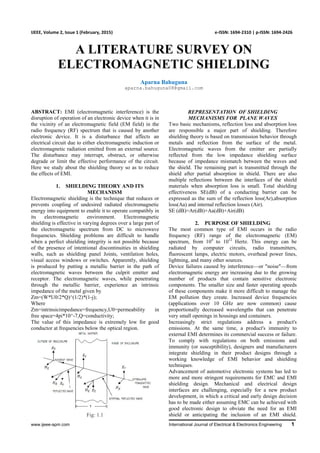
- 1. www.ijeee-apm.com International Journal of Electrical & Electronics Engineering 1 IJEEE, Volume 2, Issue 1 (February, 2015) e-ISSN: 1694-2310 | p-ISSN: 1694-2426 A LITERATURE SURVEY ON ELECTROMAGNETIC SHIELDING Aparna Bahuguna aparna.bahuguna08@gmail.com ABSTRACT: EMI (electromagnetic interference) is the disruption of operation of an electronic device when it is in the vicinity of an electromagnetic field (EM field) in the radio frequency (RF) spectrum that is caused by another electronic device. It is a disturbance that affects an electrical circuit due to either electromagnetic induction or electromagnetic radiation emitted from an external source. The disturbance may interrupt, obstruct, or otherwise degrade or limit the effective performance of the circuit. Here we study about the shielding theory so as to reduce the effects of EMI. 1. SHIELDING THEORY AND ITS MECHANISM Electromagnetic shielding is the technique that reduces or prevents coupling of undesired radiated electromagnetic energy into equipment to enable it to operate compatibly in its electromagnetic environment. Electromagnetic shielding is effective in varying degrees over a large part of the electromagnetic spectrum from DC to microwave frequencies. Shielding problems are difficult to handle when a perfect shielding integrity is not possible because of the presence of intentional discontinuities in shielding walls, such as shielding panel Joints, ventilation holes, visual access windows or switches. Apparently, shielding is produced by putting a metallic barrier in the path of electromagnetic waves between the culprit emitter and receptor. The electromagnetic waves, while penetrating through the metallic barrier, experience an intrinsic impedance of the metal given by Zm=(W*U0/2*Q)^(1/2)*(1-j); Where Zm=intrinsicimpedance=frequency,U0=permeability in free space=4pi*10^-7,Q=conductivity; The value of this impedance is extremely low for good conductor at frequencies below the optical region. Fig: 1.1 REPRESENTATION OF SHIELDING MECHANISMS FOR PLANE WAVES Two basic mechanisms, reflection loss and absorption loss are responsible a major part of shielding. Therefore shielding theory is based on transmission behavior through metals and reflection from the surface of the metal. Electromagnetic waves from the emitter are partially reflected from the low impedance shielding surface because of impedance mismatch between the waves and the shield. The remaining part is transmitted through the shield after partial absorption in shield. There are also multiple reflections between the interfaces of the shield materials when absorption loss is small. Total shielding effectiveness SE(dB) of a conducting barrier can be expressed as the sum of the reflection loss(Ar),absorption loss(Aa) and internal reflection losses (Air). SE (dB)=Ar(dB)+Aa(dB)+Air(dB) 2. PURPOSE OF SHIELDING The most common type of EMI occurs in the radio frequency (RF) range of the electromagnetic (EM) spectrum, from 104 to 1012 Hertz. This energy can be radiated by computer circuits, radio transmitters, fluorescent lamps, electric motors, overhead power lines, lightning, and many other sources. Device failures caused by interference—or "noise"—from electromagnetic energy are increasing due to the growing number of products that contain sensitive electronic components. The smaller size and faster operating speeds of these components make it more difficult to manage the EM pollution they create. Increased device frequencies (applications over 10 GHz are now common) cause proportionally decreased wavelengths that can penetrate very small openings in housings and containers. Increasingly strict regulations address a product's emissions. At the same time, a product's immunity to external EMI determines its commercial success or failure. To comply with regulations on both emissions and immunity (or susceptibility), designers and manufacturers integrate shielding in their product designs through a working knowledge of EMI behavior and shielding techniques. Advancement of automotive electronic systems has led to more and more stringent requirements for EMC and EMI shielding design. Mechanical and electrical design interfaces are challenging, especially for a new product development, in which a critical and early design decision has to be made either assuming EMC can be achieved with good electronic design to obviate the need for an EMI shield or anticipating the inclusion of an EMI shield.
- 2. International Journal of Electrical & Electronics Engineering 2 www.ijeee-apm.com Moreover, the EMI shielding design should be optimized to meet the EMC requirements with the cost as low as possible. This also has increased the demand to selecting the correct EMI shielding materials and to develop new materials for EMI shielding applications. Many factors must be taken into account in order to arrive at the correct solution. The equation for emissions from a basic circuit is: E=1.316 AIF2/(dS). Where: E = field strength in µV/m, A = loop area in square centimeters, I = drive current in amps, F = frequency in megahertz, d = separation distance in meters, S = shielding ratio between source and point of measurement. Analyzing Equation 1, it is clear that frequency is the biggest culprit because the emissions increase as the square of the frequency (F) increases. For current (I), emissions increase linearly, which is also true for loop area (A). The distance (d) is set by the test specification, and 1.316 is a constant. The system designer has no control over these last two parameters, so they must not be considered. The equation for susceptibility is: Vi=2ΠAEFB/(300S) Where Vi = volts induced into the loop, A = loop area in square meters, E = field strength in volts per meter, F = frequency in megahertz, B = bandwidth factor (in band: B = 1; out of band: B = circuit attenuation), and S = shielding (ratio) protecting circuit. Equation 2 indicates that the susceptibility is directly proportional to loop area (A), frequency (F), and the bandwidth factor (B). Frequency (F) is dictated by the specification and the operating environment, as is the field strength (E). Of course, the engineer has no control over 2π, or 300, which is the speed of light divided by 1,000,000 for this equation. From the equations, it is possible to determine some key information. Emission Levels are: • Directly related to loop area. • Directly related to signal current. • A function of frequency squared. • Inversely related to shielding effectiveness. Susceptibility levels are: • Directly related to loop area. • Directly related to bandwidth. • Directly related to the transmitted frequency and field strength. • Inversely related to shielding effectiveness. EMI can be reduced by a number of ways: • Move components on the PCB. • Add/change ground planes. • Reduce the length of noisy PCB traces and wires. • Match driver and return circuit traces or cable lines to cancel magnetic signals And reduce loop area. • Add special components, i.e., inductors, capacitors, resistors, or combinations of these parts. • Change circuit components - less noisy components. • Add ferrite products. Ferrites will absorb the EMI energy, dissipating it as small amounts of heat, typically in microwatts. • Use special shielding techniques. Shielding, this is noninvasive and does not affect high- speed operation, works for both emissions and susceptibility. It can be a stand-alone solution, but is more cost-effective when combined with other suppression techniques such as filtering, grounding, and proper design to minimize the loop area. It is also important to note that shielding usually can be installed after the design is complete. However, it is much more cost-effective and generally more efficient to design shielding into the device from the beginning as part of the design process. It is important to keep in mind that the other suppression techniques generally cannot be added easily once the device has gone beyond the prototype stage. The use of shielding can take many forms, from RF gaskets to BLS. An RF gasket provides a good EMI / EMP seal across the gasket-flange interface. The ideal gasketting surface is conductive, rigid, galvanic-compatible and recessed to completely house the gasket. A device housed in a metal case is generally a good candidate for RF gasketing materials. When electrical and electronic circuits are in nonconductive enclosures, or when it is difficult or impossible to use RF gasketing, BLS provides the best option for EMI suppression. A properly designed and installed BLS can actually eliminate the entire loop area because the offending or affected circuit will be contained within the shield. 3. DIFFERENT WAYS OF SHIELDING 1. Single Shield:- This shield contains a single layer of metal. The layer has got particular impedance and this layer contains no air gaps. 2. Multimedia Laminated Shield:-This type of shielding contains several layer shields of different impedances and contains air gaps in between them. The shielding effectiveness of multimedia shielding can be increased by controlling the impedance of the materials and thickness. 3. Isolated Double Shield:- In a big shielding enclosure a very high shielding is normally provided with double isolated conducting metal sheets separated by a inner core made up of dry plywood. Plywood does not contain any water and can be considered as a low loss dielectric with zero conductivity. 4. Perforated Shield:- Shield that is made of a number of apertures separated by a particular spacing between them. These apertures may be circular or square in shape. The total mass of single shield is very high in comparison to wire meshshield. So as our objective demands an apron protecting human beings from EMI effects, the mass or the weight of the apron should be made very low as far as possible. The multimedia laminated shield is made of several layers, as a result width of this shield is higher than any other shields. Human apron of large width will be unmanageable for the user. Same occurs for isolated double shield. Moreover these two type of shields are not flexible enough to be used as a material of human apron. The shielding techniques mentioned above are not cost effective and user friendly except wire mesh. 4. A REVIEW OF EMI SHIELDING MATERIALS The effect of growth of electronic industry and its widespread use of electronic equipment in communications, computations, automations, biomedical, space and other purposes has led to many Electromagnetic
- 3. www.ijeee-apm.com International Journal of Electrical & Electronics Engineering 3 Interference (EMI) problems to the designers as their systems/subsystems operate in close proximity. It is likely to become more severe in future, unless designers follow EMI control methodology/ techniques to meet the EMC requirements during the design stage itself. The elimination or suppression of EMI should be a prime objective of the designer. In this paper an attempt has been made to present technical data/ details of various EMI suppression materials/ devices available in the market and simplified the job of designer to verify different catalogues and which may be directly applied to the problem and harden the system/ subsystem in compliance to EMC Standards. As the design and development proceeds, the number of available noise reduction techniques also decreases and at the same time cost of mitigating noise goes up. Hence selecting a right component in right time is very essential. EMI/ RFI SHIELDING MATERIALS EMI Shielding is the use of conductive materials to reduce radiated EMI reflection and/ or absorption. Effective placement of shielding materials reduces the level of electromagnetic energy radiated by or coupled into electronic equipment. Shielding effectiveness is a measure of the performance of the shield, expressed in decibels. Several of the metals (magnetic/ non-magnetic) are available off the shelf in sheet stock form thickness of about 1/64th inch (0.4mm) or less to about 1/8th inch (32mm) or more. Metals having thickness less than 1/64 inch are sometimes regarded as foils. Many of the high permeability metals come in foil thickness ranging from about 1 mil (25.4 micro metre) to 10 mil(254 micro metre). They are usually available in both sheet and tape form. The foil stock is also available in the form of adhesive backed foil in roll lengths typically upto 100 feet. Some of the major shielding aids and their features, product description and applications are given below IRON: Fig:1.2 Iron Wire Mesh The main features of iron wire mesh are high plasticity, toughness and weld ability, good pressure processing properties but low strength. The weaving features of IRON wire mesh are precise structure, uniform opening, good corrosion resistance and long service time. Application: Galvanized wire mesh is mostly used as window screen, industrial sieves in sugar, chemical, stone crusher industries, also in sieving grain. ALUMINUM: A unique combination of properties makes aluminum one of our most versatile wire mesh weaving materials Fig: 1.3 Aluminum Wire Mesh It is light in mass, yet some of its alloys have strengths greater than that of structural steel. It has high resistance to corrosion under the majority of service conditions and no colored salts are formed to stain adjacent surfaces or discolor products with which it comes to contact. A word of caution should be mentioned in connection with the corrosion resistant characteristics of aluminum. Direct contacts should be avoided in the presence of an electrolyte; otherwise galvanic corrosion of the aluminum may take place in the vicinity of the contact area. Where other metals must be fastened to aluminum wire cloth the use of a bituminous paint coating or insulating tape is recommended. Pure aluminum in the woven form is typically used where its light weight and corrosion resistance is more important than strength. COPPER: Fig: 1.4 Copper Wire Mesh Copper wire mesh offers excellent electrical and thermal conductivity. It is non-magnetic, anti-sparking and is resistant to atmospheric corrosion, salt air and brine. The primary usages of copper in wire cloth are in those applications requiring corrosion resistance, electrical and thermal conductivity, spark resistance and non-magnetic properties. Copper wire cloth finds wide usage in traveling water screens, radio frequency interference shielding, sugar and marine applications. Copper applications are limited due to its low tensile strength, poor resistance to abrasion and common acids. REFERENCES [1] EMI and its effects byBy Dr. NagiHatoum, M.D., M.S.E.E. Wednesday, March 07, 2007. [2] The Theory of the Electromagnetic Field by David M. Cook
- 4. International Journal of Electrical & Electronics Engineering 4 www.ijeee-apm.com [3] Principles of Electromagnetics by Mathew N.O.Sadiku, Pearson Publication. [4] Electromagnetic Theory by William Hyatt [5] Kendall F. Casey, “Electromagnetic Shielding Behavior of Wire-Mesh Screens”, IEEE Transactions on Electromagnetic Compatibility, Vol. EMC-30, No. 3, pp-298-306, August 1988. [6] JayantaGhosh, T.K.Dey, MrinmoyChkraborty, “Performance of Wire-Mesh Electromagnetic Shield-an Analytical Approach” [7] Richard B. Schulz,V.C. Plantz AND D.R.Brush, “Shielding Theory and Practice” ”, IEEE Transactions on Electromagnetic Compatibility, Vol. EMC-30, No. 3, August 1988. [8] Jack E. Bridges “An update on the Circuit Approach to Calculate Shielding Effectiveness” IEEE Transactions on Electromagnetic Compatibility, Vol. EMC-30, No. 3, August 1988.