Zenerdiode ppt-111103222100-phpapp02
•Download as PPTX, PDF•
0 likes•343 views

ziner diode

Recommended
More Related Content
What's hot
What's hot (20)
Similar to Zenerdiode ppt-111103222100-phpapp02
Similar to Zenerdiode ppt-111103222100-phpapp02 (20)
Recently uploaded
Recently uploaded (20)
Zenerdiode ppt-111103222100-phpapp02
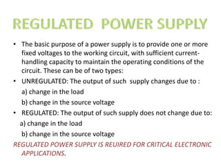
- 1. • The basic purpose of a power supply is to provide one or more fixed voltages to the working circuit, with sufficient current- handling capacity to maintain the operating conditions of the circuit. These can be of two types: • UNREGULATED: The output of such supply changes due to : a) change in the load b) change in the source voltage • REGULATED: The output of such supply does not change due to: a) change in the load b) change in the source voltage REGULATED POWER SUPPLY IS REUIRED FOR CRITICAL ELECTRONIC APPLICATIONS.
- 2. A voltage regulator circuit automatically maintains the output voltage of a power supply constant, regardless of i) a change in the load ii) a change in the source voltage + (V)S VDC LOAD - Transformer and rectifier Filter Regulator
- 3. ZENER DIODE SYMBOL: ANODE CATHODE
- 4. OUTPUT CHARECTERISTICS OF ZENER DIODE I V FORWARD BIAS REVERSE BIAS ZENER BREAKDOWN ZENER DIODE WORK AS A VOLTAGE REGULATOR IN REVERSE BIAS
- 5. ZENER DIODE CHARCETERISTICS Voltage after breakdown is also called zener voltage VFZ VZ remains nearly a constant, even though current IZ varies considerably.
- 6. The zener diode is typically connected reverse biased, in parallel with the load. Resistor Rs limits current to zener. I RS IL + IZ + vDC (IN) DZ VL RL - -
- 7. ZENER DIODE CHARACTERISTICS In the reverse bias region, a reverse leakage current flows until the breakdown voltage is reached. At this point, the reverse current, called zener current IZ , increases sharply. VR VBR IZ IR
- 8. ZENER DIODE CHARACTERISTICS In the forward region the zener diode acts like a regular silicon diode, with a 0.7 volt drop when it conducts. IF FORWARD BIAS REGION 0.7V VF
- 9. The width of depletion region is very less at high impurity concentration resulting in high electric field intensity at depletion region sufficient to break the covalent bonds and free the electrons. A large number of covalent bonds break resulting in formation of a large number of electron –hole pairs and sudden increase in the reverse current. This is known as zener effect.