
Recommended
More Related Content
What's hot
What's hot (20)
Viewers also liked
Viewers also liked (20)
Similar to Zener diode
Similar to Zener diode (20)
Recently uploaded
Recently uploaded (20)
Zener diode
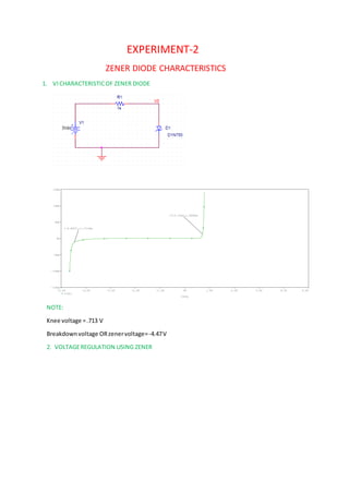
- 1. EXPERIMENT-2 ZENER DIODE CHARACTERISTICS 1. VICHARACTERISTICOF ZENER DIODE NOTE: Knee voltage =.713 V Breakdownvoltage ORzenervoltage=-4.47V 2. VOLTAGEREGULATION USING ZENER V(V0) -5.0V -4.0V -3.0V -2.0V -1.0V 0V 1.0V 2.0V 3.0V 4.0V 5.0V I(D1) -15mA -10mA -5mA 0A 5mA 10mA 15mA (-4.4657,-1.1719m) (713.191m,1.2868m)
- 2. NOTE: So fromthe curve we conclude that for aftera particularvalue of supplyvoltage (forwhich minimumZenercurrentrequiredtoensure the Zenerdiodetooperate inZenerbreakdownregion) the outputvoltage isclampedto4.5 volt.Itdoesnot change eventhe supplygoesonchanging.Thisparticular behaviouriscalledlineregulation. DISCUSSION QUESTION: 1. Compare the simulationstudyof Zenerdiode andPN junctiondiodeonthe basisof theirV-I characteristics. TakingD1N4002 as a general PN junction,the VIcharacteristicis NOTE: BREAKDOWN VOLTAGE= 100 volt FORWARDVOLTAGE = .47 volt For zenerdiode ,the VIcharacteristicis V1(V1) -10V -8V -6V -4V -2V 0V 2V 4V 6V 8V 10V V(D1:2) -1.0V 0V 1.0V 2.0V 3.0V 4.0V 5.0V TRANSFER FUNCTION V1(D6) -100V -80V -60V -40V -20V -0V-110V 15V I(D6) -60mA -40mA -20mA -0mA 20mA 40mA 60mA (-99.754,-29.426u) (468.715m,131.285u)
- 3. NOTE: ZENER VOLTAGE = 4.46 volt FORWARDVOLTAGE = .7 volt COMPARISION: PN JUNCTION ZENER Same forwardcharacteristicas Zener Same forwardcharacteristicas general PN junction Breakdownvoltage isveryhigh Breakdownvoltage (Zenervoltage) is comparativelylow Dopingiscomparativelylow Dopingiscomparativelyhigh Irreversible breakdown Reversible breakdown CONCLUSION: General diode isdesignedtoworkinforwardbiasing conditionwhilethe Zenerisforoperationin reverse region 2. A 10 V Zenerdiode (type 1N4740) placedinserieswitharesistor anda fixed12 V powersupply. What isthe currentflowingthroughthe circuitif the value of the resistoris400 ohm? V(V0) -5.0V -4.0V -3.0V -2.0V -1.0V 0V 1.0V 2.0V 3.0V 4.0V 5.0V I(D1) -15mA -10mA -5mA 0A 5mA 10mA 15mA (-4.4657,-1.1719m) (713.191m,1.2868m)
- 4. Simulationcan’tbe done asthe componentmodel isnotavailable indemoversion Kvl equation: 12-400*I-10 = 0 (asVin> Vz=10 V) I = 5 mA > 1.17mA So the correct ans is5 mA as itis greaterthanthe minimumcurrentrequiredtoputthe diode in breakdownregion. 3. Why Zenerdiode iscalledasvoltage regulator?How the ratingof Zenerdiode isdecided? It can be explainedbyconsideringthe followingcircuit So fromgraph it isclearthat whenthe supplyvoltage ismore than12V the outputdoesnot change evenif the supplyvoltage changes.The outputisfixedat4.59 V.it iscalledline regulation. V1(Vin) 0V 2V 4V 6V 8V 10V 12V 14V 16V 18V 20V 1 V(V0) 2 D(V(V0))/ D(V1(Vin)) 0V 1.0V 2.0V 3.0V 4.0V 5.0V 1 0 1.0 2.0 3.0 4.0 5.0 6.0 2 >> (12.540,4.5957) OUTPUT LOAD VOLTAGE REGULATION
- 5. So fromgraph it isclearthat whenthe loadresistance ismore than500 Ohmthe outputvoltage remainconstantirrespectiveof increase inloadresistance ordecrease inloadcurrent.Thisiscalledload regulation.The minimum500 Ohmvalue ensuresthe Zenertoworkinbreakdownregion. NOTE: load regulation specification defines how close the series resistance ofthe output is to 0 ohms - the series resistance ofan ideal voltage source. SELECTING ZENER DIODE FOR APPLICATION: IS = ID + IL Zener voltage = voltage rating of the load As we know in the process ofoperation if the load impedance increase and hence the load current decreases the current from the supplyremains same and hence the Zener current increases. Maximum Zener current >= off load current in Zener Minimum Zener current= supplycurrent-full load current Power rating = Zener voltage* Maximum Zener current 4. Obtainthe I-v characteristicof the Zenerdiode (e.g.D1N750 isa 4.7 V Zener).The voltage regulatorcircuitshown belowhasR= 1 KW. VIcharacteristic OHM 0.1K 0.2K 0.3K 0.4K 0.5K 0.6K 0.7K 0.8K 0.9K 1.0K 1 V(V0) 2 D(V(V0)) / D(I(R2)) 0V 2.5V 5.0V 1 0 0.5K 1.0K 2 >> (560.163,4.5927) RL 1k IS D7 D1N750 ID V1 16Vdc R2 1k IL
- 6. a. Findthe outputvoltage forV1 = 16 V. ans: 4.67 V b. What isthe outputvoltage whenthe supplyvoltage droppedtoV1= 8 V? ans: 4.597 V V(V0) 0V 1V 2V 3V 4V 5V 6V 7V 8V 9V 10V - I(D1) (16-V(V0))/1000 (8-V(V0))/1000 0 4m 8m 12m 16m (4.5966,3.3834m) (4.6694,11.251m)