
Recommended
More Related Content
What's hot
What's hot (20)
Similar to Original PNP Transistor BCX53-16 80V 1A AL SMD Code SOT-89 New
Similar to Original PNP Transistor BCX53-16 80V 1A AL SMD Code SOT-89 New (20)
More from authelectroniccom
More from authelectroniccom (20)
Recently uploaded
Recently uploaded (20)
Original PNP Transistor BCX53-16 80V 1A AL SMD Code SOT-89 New
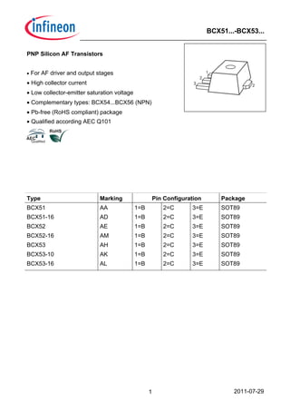
- 1. 2011-07-291 BCX51...-BCX53... 1 2 23 PNP Silicon AF Transistors • For AF driver and output stages • High collector current • Low collector-emitter saturation voltage • Complementary types: BCX54...BCX56 (NPN) • Pb-free (RoHS compliant) package • Qualified according AEC Q101 Type Marking Pin Configuration Package BCX51 BCX51-16 BCX52 BCX52-16 BCX53 BCX53-10 BCX53-16 AA AD AE AM AH AK AL 1=B 1=B 1=B 1=B 1=B 1=B 1=B 2=C 2=C 2=C 2=C 2=C 2=C 2=C 3=E 3=E 3=E 3=E 3=E 3=E 3=E SOT89 SOT89 SOT89 SOT89 SOT89 SOT89 SOT89
- 2. 2011-07-292 BCX51...-BCX53... Maximum Ratings Parameter Symbol Value Unit Collector-emitter voltage BCX51 BCX52 BCX53 VCEO 45 60 80 V Collector-base voltage BCX51 BCX52 BCX53 VCBO 45 60 100 Emitter-base voltage VEBO 5 Collector current IC 1 A Peak collector current, tp ≤ 10 ms ICM 1.5 Base current IB 100 mA Peak base current IBM 200 Total power dissipation TS ≤ 120 °C Ptot 2 W Junction temperature Tj 150 °C Storage temperature Tstg -65 ... 150 Thermal Resistance Parameter Symbol Value Unit Junction - soldering point1) RthJS ≤ 15 K/W 1For calculation of RthJA please refer to Application Note AN077 (Thermal Resistance Calculation)
- 3. 2011-07-293 BCX51...-BCX53... Electrical Characteristics at TA = 25°C, unless otherwise specified Parameter Symbol Values Unit min. typ. max. DC Characteristics Collector-emitter breakdown voltage IC = 10 mA, IB = 0 , BCX51 IC = 10 mA, IB = 0 , BCX52 IC = 10 mA, IB = 0 , BCX53 V(BR)CEO 45 60 80 - - - - - - V Collector-base breakdown voltage IC = 100 µA, IE = 0 , BCX51 IC = 100 µA, IE = 0 , BCX52 IC = 100 µA, IE = 0 , BCX53 V(BR)CBO 45 60 100 - - - - - - Emitter-base breakdown voltage IE = 10 µA, IC = 0 V(BR)EBO 5 - - Collector-base cutoff current VCB = 30 V, IE = 0 VCB = 30 V, IE = 0 , TA = 150 °C ICBO - - - - 0.1 20 µA DC current gain1) IC = 5 mA, VCE = 2 V IC = 150 mA, VCE = 2 V, BCX51...BCX53 IC = 150 mA, VCE = 2 V, BCX53-10 IC = 150 mA, VCE = 2 V, BCX51-16...BCX53-16 IC = 500 mA, VCE = 2 V hFE 25 40 63 100 25 - - 100 160 - - 250 160 250 - - Collector-emitter saturation voltage1) IC = 500 mA, IB = 50 mA VCEsat - - 0.5 V Base-emitter voltage1) IC = 500 mA, VCE = 2 V VBE(ON) - - 1 AC Characteristics Transition frequency IC = 50 mA, VCE = 10 V, f = 20 MHz fT - 125 - MHz 1Pulse test: t < 300µs; D < 2%
- 4. 2011-07-294 BCX51...-BCX53... DC current gain hFE = ƒ(IC) VCE = 2 V 10 10 10 10 BCX 51...53 EHP00440 h mA0 1 3 4 FE 310 102 010 5 5 101 210 5 100 25 -50 5 5 5 CΙ ˚C ˚C ˚C Collector-emitter saturation voltage IC = ƒ(VCEsat), hFE = 10 0 0.4 0.8 BCX 51...53 EHP00441 VCE sat V mA 10 4 1 10 10 10 2 10 10 3 10 ΙC 5 5 5 10 0 0.2 0.6 100 25 -50 ˚C ˚C ˚C Base-emitter saturation voltage IC = ƒ(VBEsat), hFE = 10 10 0 0.6 BCX 51...53 EHP00443 VBE sat 10 mA 10 10 10 4 3 2 1 0 5 5 5 V0.2 0.4 0.8 1.0 1.2 100 25 -50 CΙ ˚C ˚C ˚C Collector current IC = ƒ(VBE) VCE = 2V 10 0 0.6 BCX 51...53 EHP00437 VBE 10 mA 10 10 10 4 3 2 1 0 5 5 5 V0.2 0.4 0.8 1.0 1.2 100 25 -50 CΙ ˚C ˚C ˚C
- 5. 2011-07-295 BCX51...-BCX53... Collector cutoff current ICBO = ƒ(TA) VCBO = 30 V 10 0 50 100 150 BCX 51...53 EHP00442 TA 5 10 10 nA 10 Ι CB0 5 5 5 10 10 4 3 2 1 0 -1 max typ ˚C Transition frequency fT = ƒ(IC) VCE = 10 V 10 10 10 10 BCX 51...53 EHP00439 f mA MHz 0 1 2 35 T 310 102 110 5 5 5 CΙ Total power dissipation Ptot = ƒ(TS) 0 15 30 45 60 75 90 105 120 °C 150 TS 0 0.4 0.8 1.2 1.6 W 2.4 Ptot Permissible Pulse Load RthJS = ƒ(tp) 10 -6 10 -5 10 -4 10 -3 10 -2 10 0 s tp -1 10 0 10 1 10 2 10 RthJS D = 0,5 0,2 0,1 0,05 0,02 0,01 0,005 0
- 6. 2011-07-296 BCX51...-BCX53... Permissible Pulse Load Ptotmax/PtotDC = ƒ(tp) 10 -6 10 -5 10 -4 10 -3 10 -2 10 0 s tp 0 10 1 10 2 10 3 10 - Ptotmax/PtotDC D = 0 0.005 0.01 0.02 0.05 0.1 0.2 0.5
- 7. 2011-07-297 BCX51...-BCX53...Package SOT89 Reel ø180 mm = 1.000 Pieces/Reel Reel ø330 mm = 4.000 Pieces/Reel Package Outline Foot Print Marking Layout (Example) Standard Packing 0.8 0.8 2.0 1.01.22.5 0.7 0.45 +0.2 1) Ejector pin markings possible 1.5 3 0.2 -0.1 B 0.25 1) ±0.05 45˚ 0.15 2.5±0.1 4±0.25 M B B 0.15 ±0.10.35 ±0.21MAX.10˚ 1.5±0.1 ±0.21.6 -0.15 +0.1 2.75 ±0.14.5 ±0.11 x3 0.2 MAX. 1) 1 2 3 8 0.2 4.3 1.6 4.6 12 Pin 1 2005, June Date code (YM) BAW78D Type code Pin 1 Manufacturer
- 8. 2011-07-298 BCX51...-BCX53... Edition 2009-11-16 Published by Infineon Technologies AG 81726 Munich, Germany 2009 Infineon Technologies AG All Rights Reserved. Legal Disclaimer The information given in this document shall in no event be regarded as a guarantee of conditions or characteristics. With respect to any examples or hints given herein, any typical values stated herein and/or any information regarding the application of the device, Infineon Technologies hereby disclaims any and all warranties and liabilities of any kind, including without limitation, warranties of non-infringement of intellectual property rights of any third party. Information For further information on technology, delivery terms and conditions and prices, please contact the nearest Infineon Technologies Office (<www.infineon.com>). Warnings Due to technical requirements, components may contain dangerous substances. For information on the types in question, please contact the nearest Infineon Technologies Office. Infineon Technologies components may be used in life-support devices or systems only with the express written approval of Infineon Technologies, if a failure of such components can reasonably be expected to cause the failure of that life-support device or system or to affect the safety or effectiveness of that device or system. Life support devices or systems are intended to be implanted in the human body or to support and/or maintain and sustain and/or protect human life. If they fail, it is reasonable to assume that the health of the user or other persons may be endangered.