Magnetic semiconductors: classes of materials, basic properties, central questions
•Download as PPT, PDF•
3 likes•1,897 views

Magnetic semiconductors: classes of materials, basic properties, central questions

Recommended
More Related Content
What's hot
What's hot (20)
Similar to Magnetic semiconductors: classes of materials, basic properties, central questions
Similar to Magnetic semiconductors: classes of materials, basic properties, central questions (20)
More from ABDERRAHMANE REGGAD
More from ABDERRAHMANE REGGAD (20)
Recently uploaded
Recently uploaded (20)
Magnetic semiconductors: classes of materials, basic properties, central questions
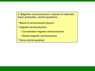
- 1. 2. Magnetic semiconductors: classes of materials, basic properties, central questions Basics of semiconductor physics Magnetic semiconductors • Concentrated magnetic semiconductors • Diluted magnetic semiconductors Some central questions
- 2. Basics of semiconductor physics Undoped (intrinsic) semiconductors: Band structure has energy gap Eg at the Fermi energy Conduction only if electrons are excited (e.g., thermally, optically) over the gap Same density of electrons in conduction band and holes in valence band: gap conduction band valence band Non-degenerate electron/hole gas in bands (i.e., no Fermi sea), transport similar to classical charged gas
- 3. Doping: Introduce charged impurities Example: replace Ga by Si in GaAs Si has one valence electron more → introduces extra electron: donor Si4+ weakly binds the electron: hydrogenic (shallow) donor state Example: replace Ga by Zn in GaAs Zn has one valence electron less → introduces extra hole: acceptor Zn2+ weakly binds the hole: hydrogenic (shallow) acceptor state EF CB VB EF CB VB excitation energy is strongly reduced (¿ Eg) conduction at lower temperatures
- 4. if impurity in crystal field has levels in the gap: deep levels (not hydrogenic), e.g., Te in GaAs both shallow and deep levels can result from native defects: vacancies, interstitials… if donors and acceptors are present: lower carrier concentration, compensation EF CB VB Increasing doping: hydrogenic impurity states overlap → form impurity band CB VB For heavy doping the impurity band overlaps with the VB or CB E 0 densityofstates VB CB EF
- 5. Magnetic semiconductors Concentrated magnetic semiconductors: Ferromagnetic CrBr3 (Tc = 37 K) Tsubokawa, J. Phys. Soc. Jpn. 15, 1664 (1960) structure: bayerite (rare and complicated) Stoichiometric Eu chalcogenides (1963) EuO: ferromagnet (Tc = 77 K) EuS: ferromagnet (Tc = 16.5 K) EuSe: antiferro-/ferrimagnet EuTe: antiferromagnet structure: NaCl good realizations of Heisenberg models with J1 (nearest neighbor) and J2 (NNN) relevant Mechanism: kinetic and Coulomb Kasuya (1970) CB (dEu) fEu FM
- 6. n-doped Eu chalcogenides: Eu-rich EuO, (Eu,Gd)O, (Eu,Gd)S, … oxygen vacancy: double donor (missing O fails to bind two electrons) Gd3+ substituted for Eu2+ : single donor The systems are not diluted: every cation is magnetic Electrons increase Tc to ~150 K (Shafer and McGuire, 1968) Mechanism: carrier-mediated, see Lecture 3 Electrons lead to metal-insulator transition close to Tc: Eu-rich EuO Torrance et al., PRL 29, 1168 (1972) One possible origin: Valence band edge shifts with T (related to exchange splitting), crosses deep impurity level
- 7. Eu1-xGdxO with x = 0% – 19%: Ott et al., cond-mat/0509722 • Eu2+ with 3d7 configuration • Gd3+ with 3d7 configuration • Gd is a donor: strongly n-type concentrated spin system: all S = 7/2, essentially only potential disorder ~magnetization more carriers & more disorder → higher Tc, more convex magnetization theory Mauger (1977)
- 8. Ferromagnetic Cr chalcogenide spinels CdCr2S4, CdCr2Se4 (Tc = 129 K) Manganites (La,X)MnO3, … structure: based on perovskite, tilted Mechanism: double exchange, due to mixed valence Mn3+ Mn4+ $ Mn4+ Mn3+ Very complicated (i.e. interesting) system! Many types of magnetic order, stripe phases, orbital order, metal-insulator transitions, colossal magnetoresistance…See Salamon & Jaime, RMP 73, 583 (2001) E. Dagotto, Science 309, 257 (2005); J. F. Mitchell et al., J. Phys. Chem. B 105, 10731 (2001)
- 9. Diluted magnetic semiconductors (DMS): Magnetic ions are introduced into a non-magnetic semiconductor host Typically substitute for the cation as 2+-ions, e.g. Mn2+ (high spin, S = 5/2) II-VI semiconductors (excluding oxides) (Cd,Mn)Te, (Zn,Mn)Se, (Be,Mn)Te… zinc-blende structure studied extensively in 70’s, 80’s Mn2+ is isovalent → low carrier concentration • usually paramagnetic or spin-glass (antiferromagnetic superexchange) • ferromagnetism hard to achieve by additional homogeneous doping • ferromagnetic at T < 4 K employing modulation p-doping (acceptors and Mn in different layers): Haury et al., PRL 79, 511 (1997) Mn2+ additional dopand
- 10. Inverse susceptibility Haury et al., PRL 79, 511 (1997) Tc Significant p-doping is required to overcome antiferromagnetic superexchange – mechanism? Hint: anomalous Hall effect and direct SQUID magnetometry find very similar magnetization → holes couple to local moments carrier-mediated ferromagnetism Anomalous Hall effect: in the absence of an applied magnetic field (due to spin-orbit coupling) • ferromagnetism with Tc = 2.5 K in bulk p-type (Be,Mn)Te:N Hansen et al., APL 79, 3125 (2001)
- 11. Oxide semiconductors (Zn,X)O wurtzite, (Ti,X)O2 anatase or rutile, (Sn,X)O2 cassiterite Wide band gap → transparent ferromagnets (Zn,Fe,Co)O: Tc ¼ 550 K Han et al., APL 81, 4212 (2002) • intrinsically n-type (Zn interstitials) • no anomalous Hall effect Not carrier-mediated ferromagnetism, possibly double exchange in deep (Fe d) impurity band? But Theodoropoulou et al. (2004) see anomalous Hall effect… Is ferromagnetism effect of “dirt” (Co clusters)? Many papers report absense of ferromagnetism – strong dependence on growth!
- 12. Rutile (Ti,Co)O2: Tc > 300 K Toyosaki et al., Nature Mat. 3, 221 (2004) Strong anomalous Hall effect depending on electron concentration → carrier-induced ferromagnetism Question: Why is Tc high for this n-type compound? Why not? Electrons in CB: mostly s-orbitals, exchange interaction between s and Co d-orbitals is weak (no overlap, only direct Coulomb exchange) Anomalous Hall effect n-type Controversial
- 13. III-V bulk semiconductors (In,Mn)As, (Ga,Mn)As, (Ga,Mn)N, (In,Mn)Sb,… zinc-blende structure focus of studies since ~ 1992 Problem: low solubility of Mn → low-temperature MBE: up to ~ 8% of Mn Mn2+ introduces spin 5/2 and hole (shallow acceptor) → high hole concentration, but partially compensated: • substitutional MnGa: acceptors • antisites AsGa: double donors • Mn-interstitials: double donors Ferromagnetic samples are p-type (In,Mn)As: Ohno et al., PRL 68, 2664 (1992)
- 14. Key experiments on (Ga,Mn)As: Ferromagnetic order Ohno, JMMM 200, 110 (1999) insulating metallic bad sample hard ferromagnet Tc ~ Mn concentration (importance of carrier concentration?) metal-insulator transition at x ~ 3%
- 15. with Mn doping: Ohno, JMMM 200, 110 (1999) with annealing: Hayashi et al., APL 78, 1691 (2001) Metal-insulator transition at T = 0 highmetallic insulating/localized low typical for disorder-induced (Anderson) insulator
- 16. Anomalous Hall effect Hall effect in the absence of an applied magnetic field (in itinerant ferromagnets, due to spin-orbit coupling) Omiya et al., Physica E 7, 976 (2000) anomalous Hall effect normal Hall effect: roughly linear in B (RH / B) B (T) saturation of magnetization
- 17. (In,Mn)As: Ohno et al., PRL 68, 2664 (1992) (Ga,Mn)As: Ruzmetov et al., PRB 69, 155207 (2004) anomalous Hall resistivity ~ magnetization → holes couple to Mn moments
- 18. Resistivity maximum at Tc Very robust feature: maximum or shoulder in resistivity Potashnik et al., APL 79, 1495 (2001) Ga+ -ion implanted (Ga,Mn)As: highly disordered Katoetal.,Jap.J.Appl. Phys.44,L816(2005)
- 19. Defects MBE growth of (Ga,Mn)As with As4 ! As2 cracker leads to enhanced Tc (110 K ! 160 K): Edmonds et al., Schiffer/Samarth group → control of antisite donors Mn interstitials detected by X-ray channeling Rutherford backscattering Yu et al., PRB 65, 201303(R), 2002 X rays MnI tilt angle Here: about 17% of Mn in tetrahedral interstitial sites
- 20. Curie temperature Tc Ku et al., APL 82, 2302 (2003) annealing increases Tc highest Tc for thin samples interpretation: donors (Mn interstitials) move to free surface and are “passivated” Sørensen et al., APL 82, 2287 (2003) hole concentration Tc depends roughly linearly on hole concentration p similar results from Be codoping carrier-mediated ferromagnetism
- 21. Mathieu et al., PRB 68, 184421 (2003) Annealing dependence of magnetization curve magnetization curves change straight/convex (upward curvature) → concave (downward curvature, mean-field-like) degradation for very long annealing (precipitates?) Potashnik et al., APL 79, 1495 (2001)
- 22. Wide-gap III-V DMS (Ga,Mn)N (wurtzite): Tc up to 370 K, Reed et al., APL 79, 3473 (2001) Anomalous Hall effect Resistivity Looks similar to (Ga,Mn)As, except for high Tc and weak resistivity peak Sonoda et al. (2002) report Tc > 750 K, but no anomalous Hall effect → inhomogeneous?
- 23. (Ga,Cr)N, (Al,Cr)N: Tc > 900 K, Liu et al., APL 85, 4076 (2004) Highly resistive (AlN) or thermally activated hopping (GaN) → localized (d-) impurity levels Different mechanism of ferromagnetism? Results on wide-gap III-V DMS are controversial
- 24. group-IV semiconductor: MnxGe1–x structure: diamond x < 4%, Tc up to 116 K Park et al., Science 295, 651 (2002) Tc » x highly resistive Some reports on ferromagnetism in Mn or Fe ion-implanted SiC and Mn implanted Si (Tc > 400K); not for diamond strong disorder
- 25. IV-VI semiconductors (Sn,Mn)Te, (Ge,Mn)Te, (Pb,Mn)Te etc. structure: NaCl narrow gap, p-type semiconductors Ge1–xMnxTe: Cochrane et al., PRB 9, 3013 (1974) x = 0.01 Tc = 2.3 K … … x = 0.50 Tc = 167 K good Mn solubility, highly p-doped, a metal at high x (Pb,Mn)Te: low hole concentration, no ferromagnetism, spin glass? (Pb,Sn,Mn)Te: Story et al., PRL 56, 777 (1986) magnetic interaction is sensitive to hole concentration and long ranged x = 0.5 T = 4.2 K magnetic field magnetization
- 26. Chiral clathrate Ba6Ge25–xFex Li & Ross, APL 83, 2868 (2003) x ¼ 3, Tc = 170 K highly disordered, reentrant spin-glass transition at Ts = 110 K Tetradymite Sb2–xVxTe3: layered narrow-gap DMS Dyck et al., PRB 65, 115212 (2002) x up to 0.03, Tc ¼ 22 K intrinsically strongly p-doped probably isovalent V3+ Similar to III-V DMS Tc
- 27. Carbon nanofoam: C structure: highly amorphous low-density foam produced by high-energy laser ablation (not an aerogel) strongly paramagnetic, indications of ferromagnetism, mostly at T < 2K, semiconducting with low conductivity Rode et al., PRB 70, 054407 (2004) weak hysteresis T = 1.8 K Possible origin: sp2 /sp3 mixed compound → unpaired electrons
- 28. III-V heterostructures (towards applications) (In,Mn)As field-effect transistor Ohno et al., Nature 408, 944 (2000) shift of Tc with gate voltage and thus with hole concentration: carrier-mediated ferromagnetism VG (In,Mn)As VG
- 29. p-doped (Ga,Mn)As δ-doped layer Nazmul et al., PRL 95, 017201 (2005) Al0.5Ga0.5As Al0.5Ga0.5As:Be GaAs 0.5 monolayer MnAs 2DHG |ψ|2 allows higher local concentration of Mn tail of hole concentration of 2DHG in δ layer Tc up to 250 K quasi-two-dimensional ferromagnet (interdiffusion?)
- 30. Some central questions In some DMS ferromagnetism is carrier-mediated – is it in all of them? In what kind of states are the carriers? Weakly overlapping deep (d-like) levels in gap or shallow levels? Impurity band or valence/conduction band? What is the mechanism? What drives the T=0 metal-insulator transition when it is observed? Magnetization curves are mean-field-like for good samples, convex or straight for bad samples – why? What causes the robust resistivity maximum close to Tc?
Editor's Notes
- 5