Nanoparticle Synthesis
•Download as PPTX, PDF•
9 likes•2,742 views

Presentation based on different techniques for nano particle synthesis.

Recommended
More Related Content
What's hot
What's hot (20)
Viewers also liked
Viewers also liked (20)
Similar to Nanoparticle Synthesis
Similar to Nanoparticle Synthesis (20)
Recently uploaded
Recently uploaded (20)
Nanoparticle Synthesis
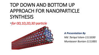
- 1. TOP DOWN AND BOTTOM UP APPROACH FOR NANOPARTICLE SYNTHESIS -for 0D,1D,2D,3D particle A Presentation By Md .Tariqul Islam-1111030 Muntaseer Bunian-1111001
- 2. Outlines of the lecture • Approach to Nanoscale Structure • Classification of Nanomaterials • Classification Top-down approach • TOP-DOWN fabrication of 1D devices • Bottom-up approach • Bottom Up Approach of 1D Devices
- 3. Classification of Nanomaterials 0D, 1D, 2D and 3D nanostructured materials Zero dimensional (atomic clusters, filaments and cluster assemblies one dimensional (multilayers) two dimensional (ultrafine- grained overlayers or buried layers) three dimensional nanostructures (nanophase materials consisting of equiaxed nanometer sized grains)
- 4. Approaches to Nanoscale Structures Junior Research Seminar: Nanoscale Patterning and Systems Teri W. Odom
- 5. Top-down approach SUBSTRATE CLEANING SPIN COAT DEVELOP PRE-BAKE EXPOSE INSPECTION POST-BAKE ETCH STRIP TOP DOWN NANOPARTICLE Process Attributes(LITHOGRAPHY) BULK MATERIAL
- 6. Top-down approach -Basic Mechanism lithography SPUN COAT EXPOSURE DEVELOP ETCH STRIP Coat, protect, expose, etch, repeat Result: Multiple patterned layers of different materials. SO RESIST BASE RADIATION(UV) MASK
- 8. TOP-DOWN fabrication of 1D devices A top-down approach to making one- dimensional quantum devices. Like resonant tunneling via quantum dots. Method pioneered by Randall and Reed at Texas instruments in the late 1980s. However, rather unsatisfactory device properties due to fabrication induced damage and poor lateral control.
- 9. Bottom-up approach The opposite of the top-down approach. • Instead of taking material away to make structures, the bottom-up approach selectively adds atoms to create structures.
- 10. Bottom-up approach BOTTOM UP NANOPARTICLE BULK WAFER PREPARATION ALTERATION AREA ADDING SEED CRYSTALS GROW/ASSEMBLE Process Attributes BOTTOM-UP
- 11. Bottom -up approach -Basic MechanismStart with bulk wafer Alter area of wafer where structure is to be created by adding polymer or seed crystals or other techniques. Grow or assemble the structure on the area determined by the seed crystals or polymer. (self assembly) Process Similar results can be obtained through bottom-up and top- down processes
- 13. Bottom-up fabrication of 1D devices We have developed an alternative approach, to form 1D nanowires (NWs) by a bottom-up, or selfassembling, method, allowing simple as well as highly complex structures to be formed. In most cases we combine a lithographic step such that the fabrication can be described as guided self-assembly. A special benefit of the seeded NW growth approach is that III-V materials and devices can be grown on silicon Array if Zn blend InAs nanowires with perfectly periodic twin-plane super lattice.
- 14. References Hench, L. L.; West, J. K. (1990). "The sol-gel process". Chemical Reviews 90: 33. doi:10.1021/cr00099a003. Buzea, C.; Pacheco, I. I.; Robbie, K. (2007). "Nanomaterials and nanoparticles: Sources and toxicity". Biointerphases 2 (4): MR17–MR71. doi:10.1116/1.2815690. PMID 20419892. Mnyusiwalla, Anisa; Daar, Abdallah S; Singer, Peter A (2003). "Mind the gap : science and ethics in nanotechnology". Nanotechnology 14 (3): R9. Bibcode:2003Nanot..14R...9M. doi:10.1088/0957-4484/14/3/201 Alemán, J.; Chadwick, A. V.; He, J.; Hess, M.; Horie, K.; Jones, R. G.; Kratochvíl, P.; Meisel, I.; Mita, I.; Moad, G.; Penczek, S.; Stepto, R. F. T. (2007). "Definitions of terms relating to the structure and processing of sols, gels, networks, and inorganic-organic hybrid materials (IUPAC Recommendations 2007)". Pure and Applied Chemistry 79 (10): 1801. doi:10.1351/pac200779101801.