Room temperature μ-PL from silicon photonic crystal nanocavities
•
0 likes•228 views

Light emission in crystalline silicon is the fundamental goal for the development of an all-silicon device showing efficient infrared emission at room temperature. The exploitation of optically active structural defects that generates sub-bandgap luminescence is the strategy explored here to make silicon an efficient infrared emitter around 1.5 μm.
Recommended

Recommended
More Related Content
What's hot
What's hot (20)
Viewers also liked
Similar to Room temperature μ-PL from silicon photonic crystal nanocavities
Similar to Room temperature μ-PL from silicon photonic crystal nanocavities (20)
Recently uploaded
Recently uploaded (20)
Room temperature μ-PL from silicon photonic crystal nanocavities
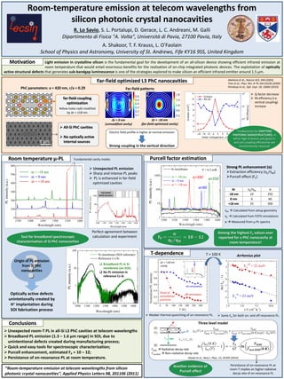
- 1. Room temperature μ-PL Room-temperature emission at telecom wavelengths from silicon photonic crystal nanocavities R. Lo Savio, S. L. Portalupi, D. Gerace, L. C. Andreani, M. Galli Dipartimento di Fisica "A. Volta", Università di Pavia, 27100 Pavia, Italy A. Shakoor, T. F. Krauss, L. O'Faolain School of Physics and Astronomy, University of St. Andrews, Fife KY16 9SS, United Kingdom Perfect agreement between calculation and experiment Light emission in crystalline silicon is the fundamental goal for the development of an all-silicon device showing efficient infrared emission at room temperature that would entail enormous benefits for the realization of on-chip integrated photonic devices. The exploitation of optically active structural defects that generates sub-bandgap luminescence is one of the strategies explored to make silicon an efficient infrared emitter around 1.5 μm. Motivation Far-field optimized L3 PhC nanocavities PhC parameters: a = 420 nm, r/a = 0.29 Tool for broadband spectroscopic characterization of Si PhC nanocavities Conclusions T-dependence Same EA for both on- and off-resonance PL. Unexpected room-T PL in all-Si L3 PhC cavities at telecom wavelengths Broadband PL emission (1.3 – 1.6 μm range) in SOI, due to unintentional defects created during manufacturing process; Quick and easy tools for spectroscopic characterization; Purcell enhancement, estimated FP ≈ 10 – 12; Persistance of on-resonance PL at room temperature. Far-field patterns Δr = -18 nm (far-field optimized cavity) Δr = 0 nm (unmodified cavity) Unexpected PL emission Sharp and intense PL peaks PL is enhanced in far-field optimized cavities Fundamental cavity modes Akahane et al., Nature 425, 944 (2003) Tran et al., Phys. Rev. B 79, 041101(R) (2009) Portalupi et al., Opt. Expr. 18, 16064 (2010) Calculated band structure Purcell factor estimation ηM Calculated from setup geometry ηC Calculated from FDTD simulations α Measured from μ-PL spectra Among the highest FP values ever reported for a PhC nanocavity at room temperature! α≈300 α≈60 α≈250 Strong PL enhancement (α) Extraction efficiency (ηC/ηM) Purcell effect (FP) Origin of PL emission from Si PhC nanocavities Optically active defects unintetionally created by H+ implantation during SOI fabrication process Δr ηC/ηM α -18 nm 22 250 0 nm 6 60 +18 nm 25 300 Onset of nonradiative processes 70° 0° Weaker thermal quenching of on-resonance PL. Yellow holes radii modified by Δr = ±18 nm far-field coupling optimization All-Si PhC cavities No optically active internal sources Electric field profile is higher at normal emission Fundamental for EMITTING PHOTONIC NANOSTRUCTURES, in which high Q-factors and good in- and out-coupling efficiencies are simultaneously required. Q-factor decrease RS efficiency (i.e. vertical coupling) increase Persistance of on-resonance PL at room-T implies an higher radiative decay rate of on-resonance PL Strong coupling in the vertical direction Hauke et al., New J. Phys. 12, 05305 (2010) Another evidence of Purcell effect Broadband PL in Si- membrane (on SOI); No PL emission in reference Cz-Si. ‘’Room-temperature emission at telecom wavelengths from silicon photonic crystal nanocavities’’, Applied Physics Letters 98, 201106 (2011) ΓRAD Radiative decay rate ΓnonRAD Non-radiative decay rate T > 100 K Arrhenius plot Three level model Δr = +18 nm cavity