1. Microstrip Power Divider Design
Theory
A power divider is a three-port microwave device that is used for power division or power combining. In an
ideal power divider, the power going into port 1 is equally split between the two output ports, and vice versa
for power combining. Figure 1 demonstrates this concept. Power dividers have applications in coherent
power splitting of local oscillator power, antenna feedback network of phased array radars, external leveling
and radio measurements, power combining of multiple input signals, and power combining of high -power
amplifiers.
Objective
To design various types of power dividers at 3 GHz and simulate the performance using HFSS.
Wilkinson Power Divider
It is not possible for any three-port network to be lossless, reciprocal and matched at all the output
ports simultaneously. In Wilkinson PD a lossy network is used to obtain matching at all three ports, but
the circuit appears to be lossless since only the reflected power from output ports are dissipated by
resistors. Further a perfect isolation between the two outputs succeed in dealing with the drawbacks of
a typical resistive divider.
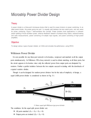
Though it can be designed for random power division but for the sake of simplicity of design, a
equal (3dB) power divider is considered as shown in Fig. 5.1.
5.1 Basic equal split Wilkinson type power divider
The conditions for the equal split power divider are:
All ports matched (S11 = S22 = S33 = 0)
Output ports are isolated (S23 = S32 = 0)
2. No power lost in going from port 1 to ports 2 and 3. (lossless when i/p at port1)
When input is at port 2 or 3 (or reflected wave from o/p ports) it behaves like a lossy network.
Equal power divisions at outputs:
2 2
21 31
1
2
S S
S-matrix at all ports:
0 1 1
1 0 0
2
1 0 0
j
S
Design Example of Wilkinson Power Divider
The schematic diagram of a 3dB equal PD is shown in Fig. 5.2(a).The power divider consists of
only three port, two output and one input port. The input feed line of 50 ohm is divided into two high
impedance arms of 70.7 ohm (50√2 Ω) which is further connected with output 50 ohm ports.
-35
-30
-25
-20
-15
-10
-5
0
0 0.5 1 1.5 2 2.5 3 3.5 4
Smiu_S11
Simu_S21
Simu_S31
Magnitude
(dB)
Frequency (GHz)
(a) (b)
Fig. 5.2 (a) Schematic of 3-dB Wilkinson type power divider (b) Scattering parameters
The structure has been simulated by IE3D EM-simulator software and considering FR4 substrate
with dielectric constant of 4.4, loss of 0.02 and height of the substrate as 1.59mm. The simulated
characteristic response is shown in the Fig. 5.2(b). The center frequency 2 GHz is taken into account
for the proposed design. Thus the length of λg/4 are found to be 20.5 mm. The above simulated
response depicts that the input power (applied at port 1) is equally divided between two output ports
(port 2 and port 3) upto 4GHz. The simulated return loss of port 1 is also found below 10dB.
3. Design Flow of Distributed T-Junction Power Divider
1. Select an appropriate substrate of thickness (h) and dielectric (εr) for the design of the power divider.
2. Calculate the wavelength λg from the given frequency specifications.
3. Synthesize the physical parameters (length & width) for the λ/4 lines with impedances of Z0 and
Z0√2. Remember that Z0 is the characteristic impedance of the microstrip line, which is 50 Ω.
Distributed T-Junction Power Divider Simulation
1. Calculate the physical parameters of the T-junction power divider. The physical
characteristics of the microstrip are as follows:
Dielectric Properties:
εr : 4.4
Height (H) : 1.6 mm
Loss Tangent (TanD) : 0.023
Frequency : 2GHz
2. Use LineCalc to determine the length and width of the 50 Ω (Z0) and 70.7 Ω (√ 2 Z0) lines.
50 Ω line:
Width = 3.04 mm
Length = 20.5 mm
70.7 Ω line:
Width = 1.61 mm
Length = 20.5 mm
3. Create a model of the T-Junction power divider in the layout window of HFSS. This can be
done using the TLines-Microstrip library.
4. 6. Open the EM Setup window to define the parameters for the simulation.
a. Define the simulation frequency from 1 GHz to 5 GHz.
b. Turn on Edge Mesh by going to Options > Mesh. Click to enable Edge Mesh.
7. Run the simulation. The results are shown in Figures 7, 8, and 9.
Find us at www.keysight.com Page
5
5. Figure 7. S(1,1), S(2,2), and S(3,3) for the power divider
Figure 8. S(2,1) and S(3,1) for the power divider
Figure 9. S(2,3) for the power divider
Find us at www.keysight.com Page 6
6. Results and Conclusions
As expected, Figure 9 shows that about half of the power goes from the input to the two output ports.
Due to loss and parasitic effects, this number is slightly less than -3 dB, meaning that a little less
than half power went to each of the output ports.
Figure 10 shows that there is significant coupling between the two output ports, which means that they
are not isolated from each other. This is one of the limitations of a T-Junction Power Divider. This will
be explored in later sections.
Wilkinson Power Divider
The Wilkinson power divider is a robust power divider with the output ports matched, with the reflected
power dissipated. This provides better isolation between the output ports when compared to the T-Junction
power divider. The Wilkinson power divider can also be used to provide arbitrary power division. The
geometry and transmission line equivalent of a Wilkinson power divider is shown in Figure
10. In this section, both a lumped element and distributed element Wilkinson Power divider will
be simulated.
Figure 10. Geometry (left) and transmission line equivalent(right)
Design of a Lumped ElementWilkinson Power Divider
Before creating the lumped element model, the capacitance and inductance values must be calculated.
Figure 11 shows the generic schematic of the Wilkinson Power Divider.
Find us at www.keysight.com Page 7
7. Figure 11. Generic schematic for Wilkinson Power Divider
From the schematic, values for the capacitance (C1 and C2) and inductance (L1 and L2) must be
determined. These values can be calculated using the formulas below.
C1=C2=
1
√2Ra∙√RbRc∙ω2
L = L = √2Ra√RbRc
2 3 ω2
L = √
R
a√R
b
R
c
1 2ω
2
R = 2√RaRb
Where
Z0 = Ra = Rb = Rc = 50 Ω
ω = 2πf, the angular frequency
Find us at www.keysight.com Page 8
8. Design Specifications
Design frequency : 3 GHz
Angular frequency : 1.88 x 10¹⁰ radians
C1 = C2 = 0.75 pF
L2 = L3 = 3.75 nH
L1 = 1.87 nH
R1 =100Ω
Lumped ElementWilkinson Power Divider Simulation
1. Create a new schematic in a new cell.
2. From the Lumped Components library, select the appropriate components. Click to place them in
the schematic, as shown in Figure 12.
Figure 12. Competed schematic for Wilkinson Power Divider
3. Set up the S-Parameter simulation from 1 GHz to 5 GHz with a step size of 0.01 GHz. Perform
the simulation and observe the responses shown in Figures 13, 14, and 15.
Find us at www.keysight.com Page 9
9. Figure 13. S(1,1), S(2,2), and S(3,3) for the power divider
Figure 14. S(2,1) and S(3,1) for the power divider
Figure 15. S(2,3) for the power divider
Find us at www.keysight.com Page 10
10. Results and Observations
Figure 13 shows that there is very little reflection into each port at the design frequency of 3 GHz. Figure
14 shows that there was also about half power going from the input port into each of the output ports.
Note that the schematic simulation does not take into account the effect that the layout will have on the
results. This will be shown in a later simulation. Figure 15 also shows that there is little coupling
between the two output ports. This is a direct result of adding the isolation resistor.
Design of Distributed Wilkinson Power Divider
1. Calculate the physical parameters of the Wilkinson Power Divider using the electrical parameters
given at the beginning of this chapter. The physical parameters for both the 50 Ω (Z0) and 70.7 Ω (√2 Z0) can be synthesized using LineCalc. The results are shown below:
50 Ω line:
Width = 2.9 mm
Length = 13.4 mm
70.7 Ω line:
Width = 1.5 mm
Length = 13.8 mm
2. The layout from the T-junction power divider will be used for the Wilkinson power divider. However,
an isolation resistor of 2Z0 is needed. This will be added when doing EM/circuit co-simulation, as we
are using a discrete component to represent the resistor. Copy the layout from the T-junction power
divider cell into a new cell for the distributed layout of the Wilkinson power divider.
3. Since the isolation resistor will be added between the outputs, add a port between each of the 50 Ω
and 70.7 Ω lines. The layout is shown in Figure 16.
Figure 16. Layout for power divider shown with Ports 4 and 5 added
4. When a new port is created, it is set to 50 Ω by default. However, because Ports 4 and 5 will be
connected to a discrete component in the schematic view, the ports need to be defined as having infinite
impedance. To do this, open the Port Editor (next to the Substrate icon or EM > Port Editor). Change
Ref Impedance to 10000 (units are ohms) for Ports 4 and 5. This is shown in Figure 17.
Find us at www.keysight.com Page 11
11. Figure 17. Port Editor showing changed reference impedance for Ports 4 and 5
5. As with the layout, copy the emSetup from the T-junction cell and paste it into this cell. Most of
the settings will be reused.
6. Verify that the frequency sweep is from 1 GHz to 5 GHz.
7. In the Model section, enable both EM model options. Press Auto-create Now. This is shown
in Figure 18.
Find us at www.keysight.com Page 12
12. Figure 18. EM Setup with EM model options selected
8. Run the simulation.
9. While an emModel was created for the layout, a symbol is needed to do co-simulation. Go to
EM > Component > Create EM Model and Symbol. Select both options, as shown in Figure 19.
Figure 19. Creating an EM Symbol
Find us at www.keysight.com Page 13
13. 10. Create a new schematic cell. Drag and drop the emModel onto the schematic. Change the
view for the simulation to emModel (right click on the symbol, go to Component >
Choose View for Simulation).
11. Set up a S-Parameter simulation from 1 GHz to 5 GHz with a step size of 0.01 GHz.
The final schematic is shown in Figure 20.
Figure 20. Schematic showing emModel used
12. Run the simulation.
Figure 21. S(1,1), S(2,2), and S(3,3) for the power divider
Find us at www.keysight.com Page 14
14. Figure 22. S(2,1) and S(3,1) for the power divider
Figure 23. S(2,3) shown for the power divider
Results and Observations
Figure 21 shows that there is more reflection into each of the ports when compared to the discrete
component model. Figure 22 shows that there is still about half power going from the input port into each
of the output ports. Figure 23 shows that there is less coupling between the output lines when compared
with the T-junction power divider. This shows the isolation resistor was effective. None of these traces
match up exactly with the discrete element simulation. This is to be expected, as the layout-based model
takes into account electromagnetic effects, such as edge effects and added parasitics of the microstrip
layer. This will negatively impact the performance of the power divider.
Find us at www.keysight.com Page 15
15. Coplanar Waveguide T-Junction Power Divider
Coplanar waveguides (CPW) are a type of waveguide that is fabricated on a printed circuit board.
Unlike traditional schematics on a PCB, a waveguide relies on the spacing between the traces to guide
the wave through the circuit. This principle applies in a CPW T-junction power divider. The layout below
is similar to that of the T-junction power divider but must be slightly modified to operate as a waveguide.
Design Flow of CPW T-Junction Power Divider
1. Select an appropriate substrate of thickness (h) and dielectric constant (ℇr) for the design of the power divider.
2. Calculate the wavelength λg from the given formula
c
λg =
√εrf
Where
c is the velocity in air
f is the frequency of operation of the coupler
ℇr is the dielectric constantof the substrate
3. Synthesize the physical parameters (length and width) for the λ/4 CPW line with impedances of Z0 and
√2 Z0.
CPW T-Junction Power Divider Simulation
1. Calculate the physical parameters ofthe CPW T-junction power divider using the parameters from the earlier
section.Use LineCalc to synthesis the length,width,and gap of the 50 Ω (Z0) and 70.7 Ω (√2 Z0) lines.The
LineCalc windows are shown in Figures 24 and 25.The physical parameters for the lines are as follows:
50 Ω Line:
Width = 3 mm [fixed]
Gap = 0.37 mm
Length = 15.96 mm
70.7 Ω Line:
Width = 1.5 mm [fixed]
Gap = 0.69 mm
Length = 15.67 mm
Find us at www.keysight.com Page 16
16. Figure 24. LineCalc for 50 Ω line
Figure 25. LineCalc for 70.7 Ω line
Find us at www.keysight.com Page 17
17. 2. Create the structure in the layout window of ADS. It can be created using the CPW components
available in the TLines-Waveguide library. Each of the waveguide components should be a quarter
wavelength, as calculated in LineCalc. This is shown in Figure 26.
Figure 26. Layout of CPW lines
3. When placing the components, note that ground separation lines will be placed on the layout. These
lines are invisible to the simulation but provides a visual clue as to where the ground plane should be
placed. Using the Draw Rectangle tool, place the ground components outside of the ground separation
lines. To make sure that the rectangles are drawn at the appropriate gap from the waveguides, enable
the following options: Toggle Snap Enabled Mode, Toggle Intersection Snap Mode, and Toggle
Vertex Snap Mode. They are located along the top toolbar.
4. Assign pins to the layout. For each signal pin, there will be two ground pins. To make it easier to
analyze results, assign the signal pins as Ports 1, 2, and 3. The ground pins should start at Port 4.
Note that the signal pins should connect right to the waveguide component and the ground pins should
be placed right inside the edge. This is shown in Figure 27.
Find us at www.keysight.com Page 18
18. Figure 27. Layout of CPW power divider with ground plane
5. The substrate used for the waveguide will be slightly different than the previous sections because of
the location of the ground pin. Make a copy of the substrate from the previous sections and place it in
the same cell as the CPW layout. Open the Substrate Editor and make the following changes. The
final substrate properties are shown in Figure 28.
a. Right click on the dielectric (FR4) and select Insert Substrate Layer.
b. Right click on the Cover layer and select Delete Cover.
c. Change the bottom dielectric to AIR.
Find us at www.keysight.com Page 19
19. Figure 28. Substrate layout showing added air layer
6. Because there are two ground pins for each signal pin, the mapping must be changed. Open the
Port Editor (next to the substrate button on the toolbar) and make the following changes. The
final port mapping is shown in Figure 29.
a. Select Ports 4 through 9. Right click and click Delete.
b. Drag the ground pins from the Layout Pins section at the bottom to the appropriate signal port
in the S-Parameter Ports section. Before the ground pins are mapped, each signal pin will show
GND instead of the port. This indicates that a ground pin has not been selected.
Find us at www.keysight.com Page 20
20. Figure 29. Port Editor showing remapped ground pins
7. Create a copy of the EM Setup from previous sections. Set the simulation frequency range as
2.6 GHz to 3.4 GHz. Ensure that Edge Mesh is enabled (Options > Mesh). Note that the
frequency span is smaller than in previous sections. This is because the simulation will require
more time because the structure is larger than in previous sections.
8. Run the simulation. When running the simulation, a warning might pop up stating that polyline
edges were found on the strip layer. This refers to the ground separation lines in the layout. This is
not a problem, as the ground separation lines are invisible to the simulation.
Figure 30. S(1,1), S(2,2), and S(3,3) for the power divider
Find us at www.keysight.com Page 21
21. Figure 31. S(2,1) and S(3,1) for the power divider
Figure 32. S(2,3) for the power divider
Find us at www.keysight.com Page 22