PERFORMANCE ANALYSIS OF D-FLIP FLOP USING CMOS, GDI, DSTC TECHNIQUES
First_Bin_Jan_2015
1. Block diagram of DFD structure on top of DFT structure
Volume - 3Volume - 3
Issue - 1Issue - 1
Jan - 2015Jan - 2015
Volume - 3
Issue - 1
Jan - 2015
a newsletter for the semiconductor engineering communitya newsletter for the semiconductor engineering communitya newsletter for the semiconductor engineering community
FROM THE PRESIDENT’S DESK
Srinivas Chinamilli
DearCustomer,
At the outset, let me wish you all Health, Happiness and
ProsperityintheNewYear!
It has been 6 months since the last newsle er. We have
been very busy in this period. We have doubled our test
floor space to accommodate more ATE equipment,
handlers, SLT handlers etc. to address increasing
customer demand for tes ng more products out of our
Bangalore facility. This required a major upgrade to our
facili es including chilled water plant, compressed air
and other electrical infrastructure. Kudos to our
opera ons team! They have worked very hard to make
thishappeninarecord me.
Characteriza on lab is also coming up well. Most of the
equipment have been received and the rest will be in
house by mid of February. With this, Tessolve will be able
to offer access to state of the art bench equipment to you
to address your characteriza on requirements. You will
beabletoeitherrentequipmentfromusorhaveTessolve
engineers execute on your projects to fulfill your analog,
highspeeddigitaland RF characteriza onrequirements.
Our HR team has been busy as well in aggressively hiring
engineers.Ouremployeecounthascrossed700.OurTest
Engineering and PCB Design teams have delivered end to
end solu ons for several complex devices including
baseband processors, microcontrollers, applica on
TESSOLVE SHOWCASE
Debug Time Reduc on in Next Genera on SOC
Swetha Priya Aenikapa , Sr. Design Engineer, VLSI Design
As semiconductor manufacturing technology shrinks down to 14nm, micro
architectural designs on a single SOC are becoming large & dense.
Consequently test escapes into pre & post silicon verifica on stages are posing
more challenges due to lack of internal node visibility. Eventually these test
escapesaredetectedatsystemlevel,therebyaddingtothecostofsilicon.These
systems typically contain at least 10 programmable processor cores packed into
various slices with dedicated peripheral func ons. This interface implements
the standard communica on protocols and hardware accelerators for
configurable processing tasks with DDR4 and with other micro-architectural
designs. As me to market is crucial, rou ng out bugs at such complexi es
requiremorenumberofvectorsandrun me.Acoupleofscenarioslikenonreal
me observa on technique, Silicon debugging me and visibility were faced
whichbroughtouttheinabilityof DFT.
Thus DFD (Design for Debug) is adopted as a solu on to record & monitor the
con nuous real me signal informa on on a chip. DFD provides high degree of
visibility to the internal nodes in-situ. However, limited resources like memory,
pin count and low level abstrac on threw challenges on internal observa on of
signals as integra on levels are unfamiliar to designers. To overcome this
tradeoff between hardware resource efficiency and number of signals, the
followingsolu onswerefoundtobegood.
From the President’s desk
Tessolve Showcase
1. Debug Time Reduction in Next
Generation OC
2. SOC Level Power Gratification in
VDSM Technology
3. Achieving High Accuracy in
Linearity Measurement
Tessolve Test Challenge Contest
1. High Current Load Board Design
– Consideration & Challenges
2. High Speed USB Testing in
Teradyne Test System
Contents
Advisory Committee
Srinivas Chinamilli
TNK Sundararajan
Rajakumar D
Technical Committee
Banukumar Murugesan
Ram Jonnavithula
Shanthanu Prabhu
Srinivas Prasad B.V.
Vidyut Yagnik
Velmurugan Thangaraj
Editor
Parthiban Selvaraj
Editorial Support
Saurabh Raj
Operations support
Thirumalesh Babu Murthy
S. Kiran Kumar
Editorial Team
Tessolve Semiconductor Pvt. Ltd.
Plot # 31, Electronic City,
Phase 2, Bangalore 560 100,
Karnataka, India.
Tel: +91 80 4181 2626
Your kind enquiries / feedback solicited at,
sales@tessolve.com / news@tessolve.com
www.tessolve.com
Printed and published on behalf of
processors, high precision analog and high voltage power
management products. To further strengthen our
produc onreleaseandsustainingac vi esinTaiwanand
China, we have established a partnership with a local
Taiwanese company. Our VLSI design team has grown
steadily to over 50 engineers offering solu ons in DFT,
designverifica onandphysicaldesign.
Tessolve also has been very ac ve in offering mentoring
program (as part of IESA and TIE ini a ve) to start-ups in
the IOT (Internet of Things) space. Thanks to our Systems
Designteamfortheireffortsinofferingvaluablesolu ons
tothepar cipa ngstartups.
I also congratulate our employees, Siva Vijayaraghavan
for winning at the All-India PCB Design Contest 2014
conducted by IPC India at Bangalore, and Vijay David for
successfullypresen ngapaper tled‘Robust PCB Library
development,maintenanceandpartssearch’at CDNLive
Cadence User Conference 2014 conducted by Cadence at
Bangalore.
We are con nuing to invest in growing our talent pool
and our equipment infrastructure to be able to serve you
be er and handle your increasing engineering needs.We
look forward to engaging with you a lot more and strive
evenhardertoprovidevalueaddservicesforyouin2015.
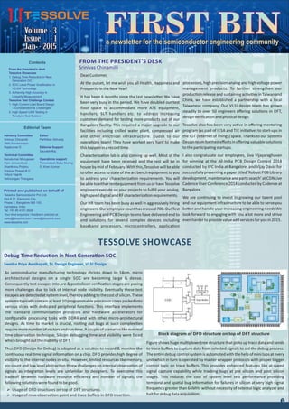
Ø Usage of DFD structures on top of DFT structures.
Ø Usage of mux-observa on point and trace buffers in DFD inser on.
Figure shows huge mul plexer tree structure that picks up trace data and sends
to trace buffers to capture data from selected signals to aid the debug process.
Theen redebugcontrolsystemisautomatedwiththehelpofminitapsatevery
unit which in turn is operated by master wrapper protocols with proper trigger
control logic on trace buffers. This provides enhanced features like at-speed
signal capture capability while tracking bugs at pre silicon and post silicon
stages. This reduces the cost of system level test performance providing
temporal and spa al bug informa on for failures in silicon at very high signal
frequency greater than 64MHz without necessity of external logic analyzer and
haltfordebugdataacquisi on.
1
2. Today semiconductor industry is emphasizing on the die size reduc on and less
metallayertechnologyprocessop ontoimprovecrossmargins.Theevalua on
of VDSM technology faces new challenges as layout dimensions con nue to
shrink whereas the number of func ons expected from SOC con nues to grow.
The uniform power distribu on throughout the chip area is the key to have
lower IR drop in the design. We need to provide reasonable number of
horizontalandver calpowerstripeswithappropriatewidthasperthedesign.
PowerPlanning
It is the process of defining the power and the GND-net of the design specifying
their structures which distributes power in the en re design. The key goals are
listedbelow.
Ø Increase rou ng resource in design.
Increase robustness of power grid network.Ø
Reduce cross talk noise.Ø
Improve IR drop.Ø
In every SOC, metal layers are distributed in power and signal routes, metal
densi es are computed such that the power grid would support aggregate
power and IR drop constraints. It creates conduc on path between power
supplyandeachcomponent.
Power Grid Methodologies
Power grid is built with metal layers that used to supply power to whole SOC
design. Based on technology op on there are one or two upper metal layers
with low resis vity. The upper most Aluminum layer (AP) has the least
resistanceandismostlyusedforpowergriddesignssuchas
Ø Power Mesh.
Power Ring.Ø
Power Rail.Ø
Power Mesh
It is one or two repeated sets of pairs in horizontal and ver cal segments that
supplypowertothecore.Themeshcanconsistofasinglenetorapa ernoftwo
ormorenetsthatrepeatatregularintervalsacrossthedesign.
Power Ring
Core Ring
The ring that enclose the core with one or more sets of power and GND rings
and provide external power from the pad ring to core structure. The top and
bo om sides and any other horizontal segments of a core ring are located on a
horizontal metal layer while le , right and other ver cal segments on ver cal
layerviaholesconnecttotheringsides.
Macro Ring
A ring that enclose one or more macros with power and GND rings providing
that macros with power. This ring does not always have 4 sides and they o en
have wire extension from one or more sides that connect to nearby power and
GND wiresofthesamenet.
Power Rail
Power and GND wires that supply power to the standard cells are placed in
standard cell rows. Power rails draw power from rings and mesh to which
they are connected. This is a single layer.
Conven onal Mesh type Power grid Methodology
Structure of Gra fica on Methods
From all the above power grid methodologies, we can limit the maximum
level of IR drop within the block and SOC level.
SOC Level Power Gra fica on in VDSM Technology
Umamaheswari Ganesan, Design Engineer, VLSI Design
The transfer characteris cs of Digital to Analog Converters (DAC) are defined
by two key parameters
Ø Integral Non Linearity (INL)
Differen al Non Linearity (DNL)Ø
INL is used to measure the accuracy of DAC output voltage when compared to
the ideal characteris cs. DNL is the maximum devia on of an actual analog
output from the ideal step value for successive input codes. In an ideal DAC one
N
least significant bit change will produce Vref/2 change in DAC output. Linearity
is a key parameter in applica ons like “Test & Measurement” which require
DAC output voltage to be highly accurate corresponding to input digital code.
Achieving High Accuracy in Linearity Measurement
Thangaraj Aruchamy, Test Engineer, Test Engineering
2
Measurementof INL and DNL erroriscalledlinearitymeasurement.
Board design for linearity measurement becomes challenging if the DAC
resolu on increases or the pin count reduces or mul ple channels are present
in a chip. If there are more channels the current drawn from reference and
power supply will increase. Mul ple channels sharing the single reference or
the power supply and reference sharing a single GND will create IR drop in
reference or GND traces. The IR drop varies with code changes since reference
currentiscodedependent.
Reduc on in LSB size demands more accurate voltage measuring instrument to
measure the change in DAC output voltage. High accuracy instruments are slow
3. TESSOLVE TEST CHALLENGE – CASE STUDIES
Inoneofourturn-keyprojectsrelatedtopowermeasurementunits,therewere
mul ple challenges like current can go up to 160 A, load board needs to be
compa ble for wafer as well as package level tes ng, needless to say cost needs
to be low too. Special power slots known as Voltage Supply Modules (VSM)
were used in TERADYNE ULTRA PA tester pla orm for this kind of high current
applica on. Two different VSM slots were used in this project where each slot
can support 81 A Max. The wafer and socket tes ng circuits had different types
of restric ons in different areas, so placement was done by considering all the
regionswhichresultedintheboardbeingsuccessfullydeployedinbothtypesof
tes ng.
Riskfactorsinthedesignexecu on
Ø Two separate Power plane layers were used for core power (VDD Power
domain).Eachlayerhad2ouncecoppertocarry160Acurrent.
Ø There are special requirements and tester mandatory lists like Force return
should be connected to the plane which connects only to the DUT ground
andallonboardcomponents/otherinstrumentgroundsshouldbeisolated.
Ø The high current plane layer is sandwiched between the two different types
of digital GND. One side had common digital GND and another had VSM
GND.TheForcereturnshouldusethe VSM GND only.
Ø So we used 2.7 mil thickness of dielectric core between power to VSM and 7
mil prepreg was used between power plane and common digital GND. So
Force return would go through separate VSM GND only due to less core
thickness.Pleasereferthebelowstackupinthefabprint.
Ø One IPC short was found during the IPCD 356 bare board net list matching
against the Gerber which is a valid one viz. an inten onal short which is
causeddueto VSM_GND and GND pinshort.
Enhancementsof VSM_GND inthecurrentdesign
Ø VSM GND slot must have a separate GND path and VSM force should not
returnthroughcommondigital GND intheoutside BGA.Specialtypeoffoot
print was created and used in this design to short between DUT GND and
VSM GND sinceithadadifferentnetname.
Ø This foot print does not have any physical component, but it will connect the
BGA GND pins and VSM GND pins alone in that par cular VSM GND plane
layers only. All other common digital GND layers will have enabled all the
GND pins including BGA and on board component's GND pins except VSM
GND pins.
Ø When such a high current return through the common GND, IR loss will be
veryhighsoseparatereturn GND isrequiredtomakeareturnpath.
Ø We cannot disconnect a few pins connec ng from plane layer due to lack of
tool possibility. So KPO Plane restric on is placed on the par cular pins
alone.
Ø Usuallyweplacethe KPO restric ononall GND pinsandviasinoutside BGA
area, in order to make all on board components' GND pins and other GND
pins disconnected in that par cular VSM GND plane layers except BGA
GND pins.
Ø But in this design we created a virtual GND short foot print to make a short
between DUT GND pins and VSM GND. So this method is useful to reduce
thecycle meforplacingthe KPO inallpinstodisconnectthepar cularpins
connec ngfromplaneandcanavoidthemanualworktoo.
Virtual GND short component used to make a short between DUT GND and
VSM GND,alsousedtoisolatethe GND pinsoutside BGA.
High Current Load Board Design – Considera on & Challenges
Selvaraj.S, PCB Design Engineer, PCB Division
VoltageSupplyModule:
This is special type of ground instrument which works at 6V/80A ra ng. Special
requirementsforthispowersupplyisthattheForcelowshouldbeconnectedto
the plane which connects only to the DUT GND and all on board
components/otherinstrument GND shouldbeisolated.
Force high and Sense high are supposed to be shorted near the C load array. We
have used 241 capacitors of 0.1uf, 31 capacitors of 22uf magne cally coupled to
provide the required decoupling. In order to achieve the plane impedance for
mul ple GND layers with high current applica on we have used a number of
low ESR capacitorstohavehighcapacitance.
Cri calsignals:
Ø PCIE signals totally 55 RF PORTS were used for this device tes ng.
Ø TSC, Touch Screen, loop back - both transmi er and receiver are looped
back to BGA itself.
Ø XG_PLL RF SIGNALS.
3
and expensive. Low accuracy instruments require on-board circuitry like high
resolu on pedestal DACs, PGAs, buffers, noise reduc on circuits and filters.
On-board components such as OPAMPS, switches and relays should be
selected based on the offset error, gain error, CMRR, PSRR, on-resistance and
capacitance. These have to be calibrated to obtain high accuracy. PCB rou ng
and ground isola on also need to be done with great care. In addi on
parameters like dri in reference voltage, GND shi and contact resistance of
thesocketalsoneedtobeconsideredforimprovinglinearitymeasurement.
Dri inreferencevoltage
Thereferencegenera oncircuitshouldhavelowtemperaturedri ,lowlineand
load regula ons, good long term stability and low noise. Any dri in reference
will increase the INL value. Hence, dri in reference should be less than half
LSB. Reference traces should be protected with guard traces. This will avoid
noise affec ng reference signal to change. Kelvin connec on should be used to
avoid IR drops.
GND shi &Socketcontactresistance
The GND shi depends on code change and is avoided by using star connec on
and GND buffer. As shown in the figure above, GND voltage is increasing with
respect to code and INL is reaching 1.6 LSB for 1 LSB DAC. Dri in GND directly
causesdri inreferencevoltage.Socketcontactresistanceshouldbelow.
4. Tessolve Semiconductor Pvt. Ltd.,
Excellence - 5th Floor,
104, Race course road,
Coimbatore - 641018,
Tamilnadu, India.
Tel: +91 422-2221199
Fax: +91 422-2490573
Tessolve DTS Inc.,
830 Stewart Drive Suite 221,
Sunnyvale, CA 94085.
Tel : +1 408 865 0873
Fax : +1 408 865 0896
Tessolve Engineering Services Pte Ltd.,
23 Serangoon North Ave 5,
#05-00 Ban Teck Han Centre,
Singapore 554530
Tel : +65 62979613
Fax: +65 62956355
Conclusion
This design had lots of challenges like placing the components, cri cal signals
rou ng, power and GND plane design, making the board work for both wafer
and package level tes ng etc. The exper se gained from this design gives us
confidenceto handle upcoming projects at ease. This method will also be useful
whiledesigningfloa nginstrumentforhighcurrentapplica ons.
High Speed USB Tes ng in Teradyne Test System
Karthik Chellappa, Test Lead, Test Engineering
Herewediscusshowtotestahighspeed USB2.0onTeradynetestpla orm.The
tests include both edge search and digital capture tests for TEST0NACK/ OTG
hosttransferandtestpacketinwhichatleast 32000samplesaretobecaptured
using the digital capture Instrument in Octal mode ming.High speed USB
tes ng is conducted at 480MHz. Only 4 pins are allowed to operate up to
800MHz in Octal mode ming. The captured 32 bit word has to be post
processed to extract the two bit informa on using DSP compute block. The test
meforthistestisexpectedtobehigherwhenwegowithlinearsearchmethod
by sweeping the r2 edge from minimum to maximum in few pico seconds
interval and get the best edge to proceed for the digital capture test. This uses
the r2 edge which has the maximum width in the edge search algorithm. Here
we describe the Interpola on method in which the edge can be es mated so
that the overall test me for the test can be op mized. The method could be
extensively used where the non-determinis c characteris cs occurs within the
clockperiod.
USB Edge Search Rou ne
The USB Edge search rou ne will do two levels of search algorithm sweeping
the r2 edge from minimum to maximum inside one clock period to find the
window within the range. The second loop will do a similar search within the
windowto find the flat region within the windowfound using the coarse search.
Edgesearchalgorithmisexecutedforallthethreetests.
Ø OTG Host transfer.
Ø TEST0NAK.
Ø TEST PACKET test and will help to find the edge to be used for the DSIO
rou ne.
The test uses linear search algorithm which takes more me to sweep the en re
rangeandaswealsohaveanouterloopfortwostepsvarying the VOD,theedge
search rou ne suffers severe test me consump on before proceeding to the
DSIO test.
Interpola on
Interpola on method using the Spline method or linear interpola on will help
to es mate or approximate the range to be chosen for the edge search
algorithmratherthansweepingtheen rerange
Ø Once the edge is iden fied based on the interpola on method and the
varia on/non-determinis c situa on happens in the device in case of USB
canbeapproximatedtogetreduc oninthetest me.
Ø Based on the verifica on using the spec search/shmoo method in finding
the window for 5 to 10 parts will ensure the margin that is available in the
edgeplacement.
Ø The sync pulse verifica on which has 127 samples of 10 toggling in the
USB_DP will ensure the communica on/handshake happening between
thetester/USB PHY.
Ø The inter packet gap between the test packets will be ignored and only the
usefulinforma onwillbecomparedagainstthepacketsent.
Ø If the error is zero for all 2bit samples (127 in the case of the TEST0NACK
and the OTG transfer) and 32567 for the TESTPACKET will ensure the USB
highspeedtestsare OK.
The test technique will be useful to quickly react to the non-determinis c
behavior of the device within a clock period and will definitely help to save
considerableamountoftest meintheproduc onenvironment.
Your kind enquiries / feedback solicited at : sales@tessolve.com / news@tessolve.com
www.tessolve.com 4
Tessolve Semiconductor Pvt. Ltd.
Plot # 31, Electronic City,
Phase 2, Bangalore 560 100,
Karnataka, India.
Tel: +91 80 4181 2626
Fax: +91 80 4120 2626