![Implementation Of The Binary Multiplier On CPLD Using Reversible Logic Gates.
DOI: 10.9790/2834-1201034042 www.iosrjournals.org 41 | Page
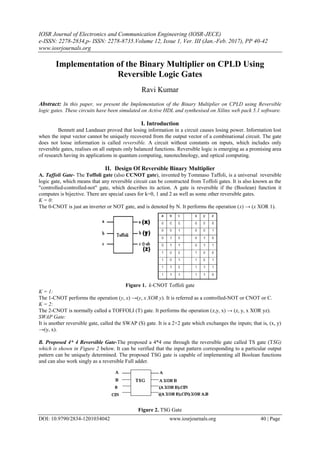
C. Reversible Logic- Landauer's Principle first argued in 1961 by Rolf Landauer of IBM, holds that "any
logically irreversible manipulation of information, such as the erasure of a bit or the merging of two computation
paths, must be accompanied by a corresponding entropy increase in non-information bearing degrees of freedom
of the information processing apparatus or its environment". Specifically, each bit of lost information will lead to
the release of an amount kT ln 2 of heat, where k is the Boltzmann constant and T is the absolute temperature of
the circuit. On the other hand, if no information is erased, the computation may in principle be achieved which is
thermodynamically reversible and require no release of heat. This has led to considerable interest in the study of
reversible computing.
III. Proposed Reversible Multiplier Architecture
The proposed reversible nxn bit parallel multiplier architecture is an improvement over reversible array
multiplier. Similar multiplier architecture in conventional arithmetic (logic) has been reported but the proposed
one is totally based on reversible logic and reversible cells as its building block. The working of the multiplier
can be deeply understood by considering a binary tree having N leaf nodes (equivalent to N partial sums) which
are merged to form their N/2 parents (equivalent to N/2 Partial Sums). These N/2 parents are again added in the
aforesaid fashion and finally, this process will be successively repeated to the get at the root of the tree (final
product). Thus, the required number of levels to compute multiplication result will be log2N. Since this
architecture requires (N-1) of N-bit reversible adders, it needs a total of N *(N-1) reversible full adder cells. So,
the worst
Figure 3. Block diagram of TSG multiplier
the propagation delay of the proposed multiplier architecture can be computed as : - d+N*d’ [log2N]
where d and d’ are the propagation delays of a Fredkin gate and reversible TSG gate (adder) respectively. By
changing the type of adder such as reversible CLA (Carry Look Ahead Adder) to reversible CPA (Carry
Propagate Adder) will make a substantial change in the propagation delay. The proposed NXN reversible
multiplier is designed for 4x4 bit. In the 4x4 multiplier, the partial products are generated in parallel using
Fredkin gates. Thus, we have 4 partial products generated.
IV. Results
The binary multiplier using Reversible logic gates was simulated on Active-HDL 5.1 software and synthesised
using Xilinx Webpack 4.1 software.
V. Conclusion
This report describes the reversible implementation of the binary multiplier on CPLD using Reversible
logic gates using Taffoli gates. The architecture of binary multiplier is specially designed to make them suitable
for reversible logic implementation. The design strategy is to reduce the number of garbage outputs, which is the
most important factor for reversible circuit cost. This approach also gives suitability for VLSI implementation
due to the use of only one kind of building block. Implementations using other standard reversible gates such as
TSG or HNG gates can also be tried. This CPLD implementation of the binary multiplier is an initial step
towards building complex reversible system, which can execute the more complicated function. Reversible logic
finds its application in areas such as quantum computing, nano-technology and optical computing and the
proposed TSG gate of efficient binary multiplier that have been derived thereof are one of the contributions to
reversible logic.](data:image/gif;base64,R0lGODlhAQABAIAAAAAAAP///yH5BAEAAAAALAAAAAABAAEAAAIBRAA7)
Recommended
Recommended
More Related Content
What's hot
What's hot (16)
Similar to Implementation of Binary Multiplier on CPLD Using Reversible Logic Gates
Similar to Implementation of Binary Multiplier on CPLD Using Reversible Logic Gates (20)
More from IOSRJECE
More from IOSRJECE (20)
Recently uploaded
Recently uploaded (20)
Implementation of Binary Multiplier on CPLD Using Reversible Logic Gates
- 1. IOSR Journal of Electronics and Communication Engineering (IOSR-JECE) e-ISSN: 2278-2834,p- ISSN: 2278-8735.Volume 12, Issue 1, Ver. III (Jan.-Feb. 2017), PP 40-42 www.iosrjournals.org DOI: 10.9790/2834-1201034042 www.iosrjournals.org 40 | Page Implementation of the Binary Multiplier on CPLD Using Reversible Logic Gates Ravi Kumar Abstract: In this paper, we present the Implementation of the Binary Multiplier on CPLD using Reversible logic gates. These circuits have been simulated on Active HDL and synthesised on Xilinx web pack 5.1 software. I. Introduction Bennett and Landauer proved that losing information in a circuit causes losing power. Information lost when the input vector cannot be uniquely recovered from the output vector of a combinational circuit. The gate does not loose information is called reversible. A circuit without constants on inputs, which includes only reversible gates, realises on all outputs only balanced functions. Reversible logic is emerging as a promising area of research having its applications in quantum computing, nanotechnology, and optical computing. II. Design Of Reversible Binary Multiplier A. Taffoli Gate- The Toffoli gate (also CCNOT gate), invented by Tommaso Taffoli, is a universal reversible logic gate, which means that any reversible circuit can be constructed from Toffoli gates. It is also known as the "controlled-controlled-not" gate, which describes its action. A gate is reversible if the (Boolean) function it computes is bijective. There are special cases for k=0, 1 and 2 as well as some other reversible gates. K = 0: The 0-CNOT is just an inverter or NOT gate, and is denoted by N. It performs the operation (x) → (x XOR 1). Figure 1. k-CNOT Toffoli gate K = 1: The 1-CNOT performs the operation (y, x) →(y, x XOR y). It is referred as a controlled-NOT or CNOT or C. K = 2: The 2-CNOT is normally called a TOFFOLI (T) gate. It performs the operation (z,y, x) → (z, y, x XOR yz). SWAP Gate: It is another reversible gate, called the SWAP (S) gate. It is a 2×2 gate which exchanges the inputs; that is, (x, y) →(y, x). B. Proposed 4* 4 Reversible Gate-The proposed a 4*4 one through the reversible gate called TS gate (TSG) which is shown in Figure 2 below. It can be verified that the input pattern corresponding to a particular output pattern can be uniquely determined. The proposed TSG gate is capable of implementing all Boolean functions and can also work singly as a reversible Full adder. Figure 2. TSG Gate
- 2. Implementation Of The Binary Multiplier On CPLD Using Reversible Logic Gates. DOI: 10.9790/2834-1201034042 www.iosrjournals.org 41 | Page C. Reversible Logic- Landauer's Principle first argued in 1961 by Rolf Landauer of IBM, holds that "any logically irreversible manipulation of information, such as the erasure of a bit or the merging of two computation paths, must be accompanied by a corresponding entropy increase in non-information bearing degrees of freedom of the information processing apparatus or its environment". Specifically, each bit of lost information will lead to the release of an amount kT ln 2 of heat, where k is the Boltzmann constant and T is the absolute temperature of the circuit. On the other hand, if no information is erased, the computation may in principle be achieved which is thermodynamically reversible and require no release of heat. This has led to considerable interest in the study of reversible computing. III. Proposed Reversible Multiplier Architecture The proposed reversible nxn bit parallel multiplier architecture is an improvement over reversible array multiplier. Similar multiplier architecture in conventional arithmetic (logic) has been reported but the proposed one is totally based on reversible logic and reversible cells as its building block. The working of the multiplier can be deeply understood by considering a binary tree having N leaf nodes (equivalent to N partial sums) which are merged to form their N/2 parents (equivalent to N/2 Partial Sums). These N/2 parents are again added in the aforesaid fashion and finally, this process will be successively repeated to the get at the root of the tree (final product). Thus, the required number of levels to compute multiplication result will be log2N. Since this architecture requires (N-1) of N-bit reversible adders, it needs a total of N *(N-1) reversible full adder cells. So, the worst Figure 3. Block diagram of TSG multiplier the propagation delay of the proposed multiplier architecture can be computed as : - d+N*d’ [log2N] where d and d’ are the propagation delays of a Fredkin gate and reversible TSG gate (adder) respectively. By changing the type of adder such as reversible CLA (Carry Look Ahead Adder) to reversible CPA (Carry Propagate Adder) will make a substantial change in the propagation delay. The proposed NXN reversible multiplier is designed for 4x4 bit. In the 4x4 multiplier, the partial products are generated in parallel using Fredkin gates. Thus, we have 4 partial products generated. IV. Results The binary multiplier using Reversible logic gates was simulated on Active-HDL 5.1 software and synthesised using Xilinx Webpack 4.1 software. V. Conclusion This report describes the reversible implementation of the binary multiplier on CPLD using Reversible logic gates using Taffoli gates. The architecture of binary multiplier is specially designed to make them suitable for reversible logic implementation. The design strategy is to reduce the number of garbage outputs, which is the most important factor for reversible circuit cost. This approach also gives suitability for VLSI implementation due to the use of only one kind of building block. Implementations using other standard reversible gates such as TSG or HNG gates can also be tried. This CPLD implementation of the binary multiplier is an initial step towards building complex reversible system, which can execute the more complicated function. Reversible logic finds its application in areas such as quantum computing, nano-technology and optical computing and the proposed TSG gate of efficient binary multiplier that have been derived thereof are one of the contributions to reversible logic.
- 3. Implementation Of The Binary Multiplier On CPLD Using Reversible Logic Gates. DOI: 10.9790/2834-1201034042 www.iosrjournals.org 42 | Page References [1]. A. De Vos, “Proposal for an implementation of reversible gates in CMOS”, International Journal of Electronics, 76, pp. 293-302, 1994. [2]. C.H.Bennett, “Logical Reversibility of Computation”, IBM J. Research and Development, pp. 525-532, November 1993. [3]. Thapliyal, M.B Srinivas and Hamid R. Arabnia, "A Reversible Version of 4 x 4-bit array multiplier with minimum gates and garbage Outputs ", 2005 International Conference on Embedded System and Applications (ESA'05), Las Vegas, U.S.A, June 2005, pp- 106-114. [4]. P. Kerntopf,” A Comparison of Logical Efficiency of Reversible and Conventional Gates”, Notes of 9th IEEE Workshop on Logic Synthesis,2000, pp. 261-269. [5]. T. Sasao and K. Kinoshita, “Conservative logic elements and their logic designs”, Synthesis and optimisation of logic system, IEEE, London, 1994.