
Recommended
More Related Content
What's hot
What's hot (20)
Similar to Transisitor amplifier
Similar to Transisitor amplifier (20)
More from HarshitParkar6677
More from HarshitParkar6677 (20)
Recently uploaded
Recently uploaded (20)
Transisitor amplifier
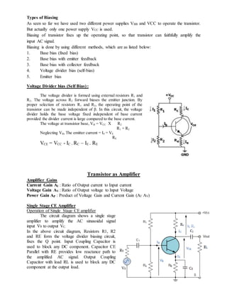
- 1. Types of Biasing As seen so far we have used two different power supplies VBB and VCC to operate the transistor. But actually only one power supply VCC is used. Biasing of transistor fixes up the operating point, so that transistor can faithfully amplify the input AC signal. Biasing is done by using different methods, which are as listed below: 1. Base bias (fixed bias) 2. Base bias with emitter feedback 3. Base bias with collector feedback 4. Voltage divider bias (self-bias) 5. Emitter bias Voltage Divider bias (Self Bias) : The voltage divider is formed using external resistors R1 and R2. The voltage across R2 forward biases the emitter junction. By proper selection of resistors R1 and R2, the operating point of the transistor can be made independent of β. In this circuit, the voltage divider holds the base voltage fixed independent of base current provided the divider current is large compared to the base current. The voltage at transistor base, VB = VCC X R2 R1 + R2 Neglecting VB, The emitter current = IE = VE RE VCE = VCC - IC . RC – IE . RE Transistor as Amplifier Amplifier Gains Current Gain AI : Ratio of Output current to Input current Voltage Gain AV : Ratio of Output voltage to Input Voltage Power Gain AP : Product of Voltage Gain and Current Gain (AI . AV) Single Stage CE Amplifier Operation of Single Stage CE amplifier The circuit diagram shows a single stage amplifier to amplify the AC sinusoidal signal input Vs to output VC. In the above circuit diagram, Resistors R1, R2 and RE form the voltage divider biasing circuit, fixes the Q point. Input Coupling Capacitor is used to block any DC component. Capacitor CE Parallel with RE provides low reactance path to the amplified AC signal. Output Coupling Capacitor with load RL is used to block any DC component at the output load.
- 2. Consider +ve half cycle of sinusoidal signal as input. Collector current IC is times IB . As voltage increases, IC increases. Increase in IC increases drop across RC . Since VC = VCC - IC . RC , VC decreases; hence for +ve half cycle, the output is –ve half cycle.This shows 180o phase shifted waveform at the output of the transistor amplifier. This is called phase reversal. Graphical Representation of Signals Frequency Response Frequency Response curve of the amplifier is a plot of voltage gain against the frequency of input signal.The amplifier provides the same amplification for few frequency range which is as shown below. Bandwidth :The range of frequency over which the voltage gain of the amplifier is equal to or greater than 70.7% of the maximum is known as 3db bandwidth of an amplifier. Bandwidth = f2 – f1 . Draw a line at 0.707 AVM , the points at which the line cuts the curve gives two frequencies. Frequency response of Single stage Amplifier is as given below. Cascading Amplifier Connecting output of 1st stage as the input of the 2nd stage is called Cascading. Need:
- 3. Amplification of single stage is not sufficient. Output or input impedance is not of required values. This is done to get required voltage, current and power gain. Types of Coupling To cascade two stages of an amplifier, Coupling circuits are used. Purpose: Transfers the AC output of one stage to the input of the next stage. Isolates the DC parameters of two consecutive stages. Types : 1. RC coupling 2. Transformer Coupling 3. Direct Coupling 1. Two stage RC coupled CE Amplifier Here, Voltage divider biasing circuit is used for each stage for stabilisation. Capacitors at Emitter provides low reactance path. Capacitor CC provides DC isolation between the stages. Frequency Response Advantages : Most convenient and least expensive multistage amplifier RC Coupling
- 4. Shows wide frequency response Provides less frequency distortion Disadvantages Provides less voltage gain due to loading effect. Has poor impedance matching Applications Used in audio amplifiers Used in public address systems 2. Transformer coupled CE Amplifier Primary winding of transformer is connected in the collector circuit of one stage, as collector load. Secondary winding is connected to the base of the next stage. Thus the AC signal developed across the primary winding induces the AC signal in the secondary winding which couples this AC signal to the base of the next stage. The DC isolation is provided by the transformer. Frequency Response Advantages : No signal power loss in the collector or base resistor, because of low winding resistance of transformer Provides higher voltage gain than RC coupled Provides excellent resistance matching between stages. Disadvantages
- 5. The coupling transformer is expensive and bulky, when operated at audio frequencies Poor frequency response At RF, produces reverse frequency distortion Produces ‘hum’ in the circuit Applications Used for impedance matching Used as a voltage amplifier and generally used in the last stage of amplifier Used in amplification of radio frequency signals 3. Direct Coupled Amplifier Here, The two stages are connected directly. It is also called as DC amplifier and used to amplify very low frequency. (below 10Hz), including zero frequency or direct current. This is used since capacitors, transformers cannot be used in very low frequency signals. Operation: The signal to be amplified is applied directly to the input of the first stage. Due to the transistor action, it appears in the amplified form across the collector resistor Q1. This voltage thendrives the base of the second transistor Q2 and the amplified output is obtained across the collector resistor of Q2. Frequency Response Advantages: Simple circuit design Less expensive Amplify very low frequency signals
- 6. Excellent frequency response Disadvantages: Cannot Amplify high frequency signals Poor thermal stability No DC isolation is provided Applications Used in electronic systems that handle signals which change very slowly with time. Some applications are Analog Computations Power supply regulators Bioelectric measurements Linear integrated circuits Transistor as an Amplifier Oscillator Definition: An oscillator is a circuit that provides a constantly, varying amplified output signal of any desired frequency. Need: When waveforms such as sine wave, square, pulse or triangular with specified frequency and amplitude is to be used in electronic systems. Range of frequency of oscillations Audio Frequency (AF) Oscillators : 20Hz – 20KHz Radio Frequency (RF) Oscillators : 20KHz – 30Mhz Very High Frequency (VHF) Oscillators: 30 -300MHz Ultra High frequency (UHF) Oscillators: 300MHz – 3GHz Microwave oscillators:3 – 30GHz. Feed Back Oscillator A part of the output is fed back to the input in proper phase and magnitude such that the effect of feedback increases the input signal. This is called Positive feedback. Feedback sinusoidal oscillator consists of two essential components: an amplifier and a feedback circuit. Feedback circuit samples a portion of the output voltage and mixes in phase with the input. Barkhausen’s criterion Considering an amplifier with feedback the gain can be defined as A’v = Av 1 - . Av Where, Av = Gain of an amplifier without feedback. Av = loop gain If . Av =1, Hence the first condition. The second condition states that phase of the loop gain should be zero or multiples of 360o. These two conditions are called Barkhausen’s criterion.
- 7. Crystal Oscillator A piezoelectric quartz crystal is used as in Crystal Oscillators. Crystal oscillator Symbol : Piezoelectric effect: when ac voltage applied across the quartz crystal, it vibrates at the frequency of the applied voltage. Conversely, if a mechanical force is applied to vibrate a quartz crystal, it generates an a.c. output. Electrical Equivalent of a Crystal : Fig below shows the electrical equivalent circuit of a crystal. It consists of a series RLC in parallel with capacitance C1 . When the crystal mounted across the a.c. source is not vibrating, it is equivalent to the capacitor C1 . When the crystal is vibrating, it acts like a tuned circuit RLC. The series resonant frequency of operation is given by fs = 1 2 L . C1 The parallel resonant frequency of operation is given by fp = 1 2 L . C where, C is parallel equivalent of C1 & C2. Since C2 is very large when compared to C1 and hence C is approximately equal to C1 . Hence fs = fp Crystal oscillator circuit Resistors R1, R2 and RE form the voltage divider biasing circuit , fixes the Q point. Crystal connected as a series element in the feedback path from collector to base. Capacitor CE parallel with RE provides low reactance path to the amplified AC signal. RFC coil provides the dc bias also couples any ac signal from affecting the output signal Cc with negligible impedance blocks dc between collector and base. Applications Used in applications where frequency stability is essential. Used in communication transmitters Personal Computers Digital watches and clock