Electronics and Communication Engineering
•
1 like•109 views

Electronics and Communication Engineering is the Branch of Engineering. Electronics and Communication Engineering field requires an understanding of core areas including Engineering Graphics, Computer Programming,Electronics Devices and Circuits-I, Network Analysis, Signals and Systems, Communication Systems, Electromagnetics Engineering, Digital Signal Processing, Embedded Systems, Microprocessor and Computer Architecture. Ekeeda offers Online Mechanical Engineering Courses for all the Subjects as per the Syllabus. Visit : https://ekeeda.com/streamdetails/stream/Electronics-and-Communication-Engineering

Recommended
More Related Content
What's hot
What's hot (20)
Similar to Electronics and Communication Engineering
Similar to Electronics and Communication Engineering (20)
More from Ekeeda
More from Ekeeda (20)
Recently uploaded
Recently uploaded (20)
Electronics and Communication Engineering
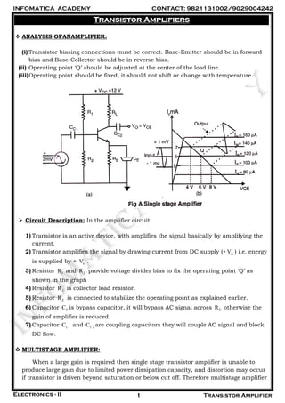
- 1. INFOMATICA ACADEMY CONTACT: 9821131002/9029004242 Electronics - II Transistor Amplifier1 Transistor Amplifiers ANALYSIS OFANAMPLIFIER: (i) Transistor biasing connections must be correct. Base-Emitter should be in forward bias and Base-Collector should be in reverse bias. (ii) Operating point „Q‟ should be adjusted at the center of the load line. (iii)Operating point should be fixed, it should not shift or change with temperature. Circuit Description: In the amplifier circuit 1) Transistor is an active device, with amplifies the signal basically by amplifying the current. 2) Transistor amplifies the signal by drawing current from DC supply (+ ccV ) i.e. energy is supplied by + ccV . 3) Resistor 1R and 2R provide voltage divider bias to fix the operating point „Q‟ as shown in the graph 4) Resistor RL is collector load resistor. 5) Resistor RE is connected to stabilize the operating point as explained earlier. 6) Capacitor EC is bypass capacitor, it will bypass AC signal across ER otherwise the gain of amplifier is reduced. 7) Capacitor C1C and 2CC are coupling capacitors they will couple AC signal and block DC flow. MULTISTAGE AMPLIFIER: When a large gain is required then single stage transistor amplifier is unable to produce large gain due to limited power dissipation capacity, and distortion may occur if transistor is driven beyond saturation or below cut off. Therefore multistage amplifier
- 2. INFOMATICA ACADEMY CONTACT: 9821131002/9029004242 Electronics - II Transistor Amplifier2 is connected; it may be two stage, three-stage amplifier. Fig. shows a three-stage transistor amplifier and the phase shift at each stage. The total gain of three-stage amplifier is calculated by a formula. TotalA = 1 2 3A A A If Gain (A) of each stage is 100 and suppose input voltage ( inV ) is u1 V then TotalA = 100 x 100 x 100 = 2 10 x 2 10 x 2 10 TotalA = 6 10 out Total in 6 6 6 6 0 V A V = 10 1μV = 10 1 10 1 10 Volt. Refer fig. each transistor produces 0 180 phase shift then total phase shift of there stage amplifier is = 180 + 180 + 180 = 0 0 0 0 0 540 (360 180 )OR (0 180 ) Output signal is 0 180 out of phase with input signal COUPLING METHODS: Basically coupling circuit is necessary avoid the shift of operating point, to block DC reverse current flow, and to couple AC signal. Coupling circuit is designed according to (i)Frequency response (ii) Impedance matching (iii) Type of input signal. There are four methods of amplifier coupling
- 3. INFOMATICA ACADEMY CONTACT: 9821131002/9029004242 Electronics - II Transistor Amplifier3 (1) R-C coupling (2) Impedance Coupling (3) Transformer Coupling (4) Direct Coupling Let us see each type with their advantage, disadvantage and typical application. (1) R-C Coupling: The Collector load resistor ( CR ) and the Coupling Capacitor ( CC ) form a coupling circuit as shown in fig (a). This type of coupling is more popular in audio amplifiers; it couples AC and blocks DC from CCV to base of the transistor as shown in fig (b) Capacitor coupling you can observe in voltage amplifier of radio receiver i.e. from volume control to A.F. amplifier. Frequency Response Of R-C Coupling: The frequency response of RC coupled amplifier is shown by fig. It also shows the experimental set up for this purpose. Frequency response tells us about the performance of a circuit against frequency variation from low to high. Frequency response is essential because it gives an idea about the range of frequency for which this coupling is suitable. The graph of output or the gain of amplifier verses frequency is known as frequency response. A signal generator is connected to apply various frequencies with small and constant input voltage to a RC coupled amplifier. The output is measured either on CRO or VTVM and graph is plotted. The curve shows 3 db curve it falls below 1F and 2F .
- 4. INFOMATICA ACADEMY CONTACT: 9821131002/9029004242 Electronics - II Transistor Amplifier4 The frequency response is flat from Z50H to Z20KHL but it is poor below Z50H above Z20 KH . The gain of amplifier is falling below Z50H and above Z20KHL . This curve can be explained as follows. (i) At lower frequencies below Z50H reactance of coupling capacitor ( CC ) is high because it is given by C 1 X 2 fC Therefore, more voltage drop takes place across it, which reduces the input thus output is poor. Similarly emitter bypass capacitor EC is less effective at these frequencies. (ii) Above Z,20 KH the coupling capacitor behaves as a short circuit because its reactance is negligible which increases the loading effect on the next stage. Similarly inter-electrode capacitance from collector to base becomes effective its equivalent capacitive reactance is low which gives negative feedback and it affects the gain of amplifier. Advantages: (i) RC coupled amplifier is suitable only for audio frequency signal Z20H to Z20KH . (ii) Soldering of RC is convenient and cost of the coupling network is least expensive. (iii) It is useful in record players, sound section of amplifiers etc. Disadvantages: (i) It is not useful for RF signal. (ii) Impedance matching is poor. (2) Impedance Coupling: In RC coupling a power loss ( 2 I R ) takes place across load resistance CR . An inductor can replace this resistance. Inductor has got high impedance for high frequency. Therefore large output AC Voltage can be developed across it and since its DC resistance is very low, DC loss is negligible. This type of coupling is not suitable for low frequencies it is useful for the high frequencies (RF) above Z20 KH . Impedance coupling is used in oscillators circuits. Disadvantages:- Inductors or RF chokes are expensive and their impedance decreases at low frequencies. The size of the inductor is also another drawback.
- 5. INFOMATICA ACADEMY CONTACT: 9821131002/9029004242 Electronics - II Transistor Amplifier5 (3) Transformer Coupling: Transformer coupling is also popular line RC coupling. In radio receivers transformer coupling is always used in IF amplifiers connecting one IF amplifier to the second IF amplifier of radio receiver. Transformer coupling serves three important purposes. (i) Output impedance of one stage matching with input impedance of the next stage. (ii) It provides isolation from one stage to next stage because there is no direct connection between primary and secondary winding of the transformer. (iii) Output voltage of one stage can be stepped up with a step up transformer. Transformer coupling also commonly used in RF amplifiers of radio and TV circuits. Fig. shows that load resistance CR is replaced by primary of transformer there is no capacitance from secondary to input of the next stage. DC isolation is achieved with secondary winding itself because DC cannot be transformed from primary to secondary. Transformer coupling with shunt capacitor across it is another way of coupling in amplifier. Such type of amplifier is known as “tuned-RF/(TRF)” amplifier. Here L-C parallel resonance principle is used which is tuned to desired frequency so the impedance of L-C circuit becomes maximum only at resonant frequency. Advantages: 1) This type of coupling is suitable for RF frequencies, as in radio circuits to amplify station signals from Z550 KH to Z1600 KH medium wave band. 2) Transformer coupling provides good impedance matching and better gain. 3) Power loss across collector load is minimized up to negligible value. Disadvantages: 1) It has poor frequency response i.e. the gain varies with frequency. 2) The size of the transformer and its high cost. 3) Amount of „hum‟ or noise is comparatively high.
- 6. INFOMATICA ACADEMY CONTACT: 9821131002/9029004242 Electronics - II Transistor Amplifier6 (4) Direct Coupling: In this method there is no coupling component, the collector of one transistor is directly connected to the base of the next transistor. These types of amplifiers are used in DC amplification or amplification of very low frequencies below 10Hz. For example, to drive an active load like DC relay, DC motor, headphones, etc. the main drawback of such amplifier is, temperature effect It is called as temperature drift it affects the biasing of transistor. Fig. shows an example of direct coupling. When light falls on LDR is resistance decreases therefore more DC voltage is developed across the base resistance BR . This change in base voltage is amplified in the collector, which drives the next transistor the collector goes low. The low collector voltage of the first transistor is applied to the base of second transistor. The low base voltage will make the second transistor OFF. Thus relay is operated in OFF state. When light is made cut-off the base voltage decreases which is amplified by the first transistor. Its collector goes high which is coupled to the second transistor. It will make the second transistor ON and thus relay is operated into ON state. In this way it couples and amplifies DC signal. Advantages: i) The coupling circuit is simple because it requires minimum resistors. ii)It is a low cost method because no coupling component is required. Disadvantages: i) It is not useful for AC high frequency signal. ii)Operating point is shifted due to temperature. POWER AMPLIFIERS: Power amplification is necessary because the output stage of any instrument required to be more powerful. It should supply maximum current and maximum voltage (I x V = Power). Fig. shows the block diagram of an amplifier stage.
- 7. INFOMATICA ACADEMY CONTACT: 9821131002/9029004242 Electronics - II Transistor Amplifier7 The output of voltage amplifier is not capable of driving the loudspeaker because of heavy load current. Similarly in radio transmitter, TV transmitter circuit, the output of amplifier is not capable of driving the antenna. Therefore a power amplifier is required to deliver maximum current with maximum voltage to drive the loudspeaker, antenna etc. They are classified into four different types i) Class A ii) Class AB iii) Class B iv) Class C i) Class A power Amplifier: The Class A power amplifier is operated at the center of the load line, as it is illustrated in fig. the operating point „Q‟ is located at the center of load line. Advantages: The output of Class A amplifier is undistorted and full cycle of input signal is amplified. Transistor conducts for 360⁰ i.e., it amplifies complete input signal. The transistor is operated in active region. Disadvantage: Refer the fig. at zero signal condition, when input signal is zero or when input signal is absent collector current of 100 mA flows through transistor and CEV (on X-axis) it is 8V therefore power loss across the transistor is lossP =8V×100mA=800mW The efficiency of class A amplifier is only 25%, it is poor efficiency.
- 8. INFOMATICA ACADEMY CONTACT: 9821131002/9029004242 Electronics - II Transistor Amplifier8 ii)Class B power Amplifier: In class B power amplifier transistor is biased at cut off as illustrated in fig. The operating point is adjusted at cut off. The result of this, under zero signal condition transistors is in cut off therefore less wastage of power takes place under zero signal condition. Advantage:- Since, only half cycle is amplified as shown, during the negative half cycle of input signal, transistor remains cut off but the efficiency increases about 78.5% because when signal is zero transistor is OFF. Current through transistor is zero. Disadvantage: Since, the transistor is biased at cut off it conducts only for positive half cycle of input signal. It remains cut off for negative half cycle as shown. The transistor amplifies only half cycle and thus extremely high distortion is produced. There is a crossover distortion. Class B Push Pull Amplifier:- The fig. shows a typical Push Pull Class B amplifier. In Positive half cycle transistor 1T is ON for 180⁰ and current flows through output transformer. Similarly in negative half cycle transistor 2T is ON and 1T is cut off it also flows through output transformer and thus in the secondary side a amplified output is developed. Push Pull arrangement eliminates much of the distortion but at the midpoint of two half cycles a distortion occur known as Crossover distortion. This crossover distortion is produced because of nonlinear characteristics of internal diode of the transistor at and below 0.6 volt.
- 9. INFOMATICA ACADEMY CONTACT: 9821131002/9029004242 Electronics - II Transistor Amplifier9 iii) Class AB Power Amplifier: It is the solution to avoid crossover distortion of class B amplifier. It‟s characteristics lies between class A and class B amplifier. It‟s operating point is located slightly above cut off as shown in fig., it is in between class A and Class B. Transistor in class AB conducts more than 180⁰ angle and less than 360⁰. The efficiency of class AB is more than class A and less than Class B push full amplifier, commonly used in radio circuit to drive the load speaker. iv) Class C Power Amplifier: In this class, transistor is conducting less than 180⁰. It‟s operating point lies beyond cut off. Advantages: Since transistor is operated for less than 180⁰ efficiency is very high about 100%. It is used in tuned amplifiers and in oscillators. Disadvantage: Extremely high distortion hence it is not useful for audio amplification. It is used in oscillator circuits. COMPARISON:- Class A Class B Class AB Class C Operating point Q located At the center At cutoff Before Cutoff Beyond cutoff Transistor conducts for 360⁰ 180⁰ More than 180⁰ Less than 180⁰ Distortion Absent Crossover Less than 50% Highest Efficiency Lowest Better Better Excellent Application Voltage amplifier Push-pull amplifier Push-pull amplifier Oscillators
- 10. INFOMATICA ACADEMY CONTACT: 9821131002/9029004242 Electronics - II Transistor Amplifier10 DIFFERENTIAL AMPLIFIER:- It is a special type of amplifier capable of amplifying the difference hence called as difference amplifier or differential amplifier. It plays very important role in “operational amplifier commonly known as “OPAMP”. It is also useful in other industrial circuits. The fig. shows the circuit diagram of differential amplifier, it is a symmetrical structure in which two identical transistors are connected with equal collector resistors. The differential amplifier has two inputs:- (i) Inverting input and (ii) Non-inverting input. The basic difference between these two is inverting input produces output 180⁰ out of phase with input while non-inverting does not produce phase shift between input and output. It has two inputs 1V and 2V the output is taken either between two collectors or from one collector with respect to ground. The fig. (3.14) shows most practical and widely used configuration, output is taken from collector of 1T with respect to ground. Differential amplifier it can be operated in different modes such as:- 1) Differential input mode 2) Common input mode 3) Single ended input mode 1) Differential input mode: In this mode signal is applied between terminal 1V and 2V and output is taken from the collector. It is called as differential input single ended output mode. As shown in figure (3.14) output is taken from either of collectors. Its output voltage is given by equation – 0 1 2V =A V -V Since. 1V is 180⁰ output of phase with 2V but equal in amplitude. 0 1 2 1V =A V -V =2AV Thus, in differential mode maximum gain is obtained, twice input voltage multiplied by gain (A).
- 11. INFOMATICA ACADEMY CONTACT: 9821131002/9029004242 Electronics - II Transistor Amplifier11 2) Common input mode: In this mode same signal is applied to both input terminals that is 1 2 0 1 2 1 1 V =V then V =A V -V =A V -V =0 it means that for common signals like noise its gain is zero it rejects unwanted noise signals DM CM A Differentialmodegain CMRR = = A Common modegain 3) Single ended input mode: In this mode, input is applied to one of the inputs and other input is grounded, output can be differential or it can be single ended. When output is single ended it is called as an OP-AMP. In OP-AMP the mode is single ended input single ended output or differential input, single ended output. TRANSISTOR AS A SWITCH:- Normally transistor is used as an amplifier where it is operated below saturation and above cut off; it is operated in active region. Another important application of transistor in digital circuits, it can be operated as a switch. In switching application the transistor is operated either is saturation or in cut off only and non in active region. It has got following advantages over normal mechanical switch. i) Low cost ii) Small size iii) High speed Let us see how transistor is used as a switch. Fig. shows a NPN transistor with emitter grounded. Input voltage is applied to the base terminal and output is taken from collector ( CEV ). Here transistor is operated either in saturation or in cut off instead of active region.
- 12. INFOMATICA ACADEMY CONTACT: 9821131002/9029004242 Electronics - II Transistor Amplifier12 SOLVED PROBLEMS 1) What is the value of collector load resistance required to set CV as 4 volts and CI as 1mA for the collector supply voltage of 6 volts in Transistor Amplifier. CC C C C CE CC C C C C CC C CC C C C -3 3 C Solution: Given V =6 V, I =1mA R = ? V = 4V Formula for collector voltageV = V -I R I R = V - V V - V R = I 6-4 = 1×10 R = 2×10 Ω= 2KΩCollector load should be 2KΩ 2) Find the total voltage gain of a three – stage amplifier in db if first stage has gain of 100 second has 300 and third has 400. o i o i o i V Solution: i) First Stage Voltage Gain in db = 20log db V = 20log100= 20×2= 40db V ii)Second Stage Voltage Gain in db = 20log db V = 20log300= 20×2.48= 49.6db V iii)ThirdStageVoltageGainin db= 20log db V = 20log 400= 20×2.60=52db Total gain = 40+49.6+52=141db