SlideShare a Scribd company logo
1 of 8
COMMON EMITTER CONFIGURATION
In CE configuration, emitter terminal is made common, while input is applied
between base and emitter and output is taken across collector and emitter.
To study the CE configuration, first consider the input circuit and plot the input
current(IB) w.r.t. input voltage between base and emitter (VBE).
Then, consider the output circuit of the CE configuration and plot the output current IC
w.r.t. output voltage between collector and emitter (VCE).
Thus, there are two characteristics for CE configuration.
i. Input characteristics
ii. Output characteristics
Circuit Diagram of CE Configuration
Following fig. shows transistor current and voltage in common emitter configuration.
The input voltage in the CE configuration is the base-emitter voltage VBE and output
voltage is the collector-emitter voltage(VCE). The input current is IB and the output
current is IC.
To obtain the input and output characteristics of the CE configuration, experimental
setup is as shown in fig.
Potentiometer R1 is used to vary the input current IB. To measure the current IB,
milliammeter is connected series as shown. Similarly, to measure the collector Current IC,
milliammeter is connected in series with potentiometer R2, in the output circuit.
Input voltage VBE is measured using a DC voltmeter connected between the base and
emitter. Output voltage VCE is measured using a DC voltmeter connected between
collector and emitter.
Input Characteristics for CE Configuration
Input characteristics are plotted by considering only the input parameters i.e. input
current IB and input voltage VBE.
Input characteristics give the relationship between base current IB and base to emitter
voltage VBE.
To obtain the input characteristics of CE configuration, voltage between collector to
emitter i.e. VCE is kept constant by adjusting the R2. Adjust VCE= 1V and keep it constant
and then increase the voltage VBE in small suitable steps of in order of 0.1V and record
the corresponding values of input current IB. Thus, we get the set of value of IB for
different values of VBE, for VCE= 1V constant.
Repeat the similar steps by keeping VCE= 5V to get the 2nd set of readings and finally by
keeping VCE= 10V to get the 3rd set of readings.
Each set of reading is plotted such that current IB is taken on Y-axis and the voltage VBE
on X-axis. Thus, we get three curves for three different values of VCE as shown in the fig.
From the input characteristics, we observe the following important points:
1. For region OA of the curve, the base current is very small. This voltage at which
we get very small base current is called as cut-in voltage or knee voltage. It is denoted
by Vk. The value of knee voltage is approximately 0.5 for silicon and 0.1V for
germanium.
2. After the cut-in voltage (i.e. after the point A) the base current increases rapidly
with small increase in the base to emitter voltage VBE.
This indicates that the dynamic input resistance is small in CE configuration.
3. Dynamic resistance(ri) is given by the ratio of change in base-emitter
voltage(VBE) to the resulting change in the base current(IB) at constant VCE.
ri=
𝑉𝐵𝐸
𝐼𝐵
VCE= constant
4. For fixed value of VBE, IB decreases as VCE increases. The increase in VCE
increases the reverse bias across the junction JC. This increases the depletion layer width
across JC, this reduces the effective base width between JE and JC and due to this the
overall base current reduces.
Output Characteristics for CE Configuration
Output characteristics is plotted by considering only the output parameters i.e.
output current IC and output voltage between collector and emitter VCE. To obtain the
output characteristic of CE configuration, the current IB is kept constant. To do this, vary
R1 to adjust base-emitter voltage VBE, which set the suitable value of current IB(say
20A). Then increase the voltage VCE in suitable steps of order of 1V by using POT R2,
then record the values of collector current IC corresponding to different values of VCE.
Plot IC on ‘Y’ axis and VCE on ‘X’ axis. Repeat similar steps for values of IB as 40A,
60A etc. to get different curves as shown in fig. IC(MA).
From the output characteristics we observe the following important points:
1. This characteristics shows relation between collector current IC and collector to
emitter voltage VCE for fixed value of IB. This characteristic is also called as collector
characteristic.
2. The output characteristic is divided into three important regions.
i. Active region
ii. Saturation region
iii. Cutoff region
3. The value of dc of the transistor can be found at any point on the characteristics
by taking the ratio IC to IB at that point.
dc=
Ic
IB
This is called as DC beta for the transistor. Similarly, if we take the ratio of change in IC
i.e. IC to change in IB i.e. IB for a fixed value of VCE then it gives AC beta i.e. ac.
ac=
IC
IB
VCE= Constant
Generally values of ac and dc are nearly equal. value is always
greater than 1.
4. From the curve it is seen that the large change in VCE causes very small change in
IC for constant IB. This indicates that the dynamic output resistance (r0) is high in CE
configuration.
r0=
VCE
Ic
5. Active region: The active region where the curves are approximately horizontal or
flat is called as Active region. Increase in voltage VCE, increases the reverse bias across
the junction JC. This increases the depletion layer width between JE and JC reduces. This
reduces the base current IC. For this reason, CE output characteristics are sloping
upwards.
6. Cutoff region: The collctor current IC is not zero, even when the base current IB is
zero. Thus there exists a small value of collector current. This is called as reverse
leakage current denoted by ICEO. Under this condition the transistor is said to be in
cutoff state.
7. Saturation region: If VCE is reduced to a small value such as 0.2V then, the
collector base junction JC gets forward biased and emitter base junction JE and JC is
already forward biased. Thus, both the junctions JE gets forward biased. This rapidly
increases the collector current IC. The region showing this is called as saturation region.
In saturation region, we cannot keep control over the current IC.
8. In the active region: If we go on increasing the value of VCE beyond certain
maximum value, then the breakdown occurs. This gives very high collector current. This
effect is called as punch through effect.
TRANSISTOR BIASING
To operate the transistor exactly in the active region it is necessary to keep the
base – emitter junction(JE) properly forward biased and collector base junction (JC)
properly reverse biased, during application of input signal to the transistor. Doing this is
called as biasing and the circuit designed to do this is called as biasing circuit. Thus
biasing of transistor makes sure that the transistor is ON and remains in the active region
where it operates linearly and provides a constant amount of voltage gain.
Biasing sets up a fixed current through transistor (IB and IC), with a fixed voltage drop,
across the transistor junctions (VBE and VCE). The proper values of these currents and
voltages force the transistor to amplify the input weak signal faithfully.
Biasing of transistor fixes the current IC and voltage VCE i.e. it fixes up a point on the
output characteristics. This point is called as operating point of transistor, denoted by Q.
It is also called as Quiescent Point.
Conditions to be fulfilled during biasing the transistor are:
1. Transistor should work in active region and cannot enter in saturation or cutoff
regions.
2. Transistor Q point should be at the central area of active region.
3. IC, IB, and VCE, VBE must be constant.
DC Load Line (Also see class notes for other methods)
The DC load line is the line on the output characteristics, which gives the values of
IC and VCE for zero input signal i.e. DC conditions. To draw the DC load line, consider
the following circuit as shown in fig.
Here,
VCC = ICRC + VCE=0
 ICRC= VCC-VCE
IC=-
1
Rc
VCE+
VCC
Rc
Comparing this equation with the equation,
y= mx +c
Which is a straight line equation. We get,
Slope (m) = -
1
𝑅𝑐
And ‘Y’- axis intercept is
c =
𝑉𝑐𝑐
𝑅𝑐
Now plotting this line on the output characteristics of transistor, we get fig as shown
below.
The straight line on the output characteristics is called as DC load line. The two end
points on the line are
VCC (on X axis) and
𝑉𝑐𝑐
𝑅𝑐
(on Y-axis).
These two points are located on the characteristics as follows:
1. When collector current IC = 0, VCE will be maximum and is given as
VCE = VCC –ICRC
VCE (Max) = VCC -0(RC)
VCE (Max) = VCC
Thus, we get one point on X-axis
2. When collector to emitter voltage VCE =0 then, IC will be maximum and it is given
as:
VCE = VCC- ICRC
0 = VCC –ICmax. RC
 Icmax =
𝑉𝑐𝑐
𝑅𝑐
Thus we get one point on the Y-axis.
Thus, connecting these two points, we get a DC load line. As shown in fig. DC load line
gives us the following information:
i. The DC load line intersects the horizontal (X) axis at point B. The point is called
as transistor cutoff point.
At this point, the values of base current IB and collector current IC are ideally zero. But
practically small reverse saturation current flows (ICEO) and the voltage VCE is highly less
than VCC.
ii. The load line intersects the vertical Y-axis at point A. This point is called as
transistor current is a maximum and the voltage VCE is very small equal to VCE(sat).
The point where the DC load line cuts the output characteristics is called as the
operating point Q as shown in fig.
This Q point fixes up the current IC and voltage VCE, so that the transistor is continuously
operated in the active region only.
As Q point is shifted upwards, the transistor is operated near the saturation and when Q
point is shift downwards then transistor is operated near cutoff and there is possibility
that the transistor can turn off at any time.
Thus, AC load line is drawn by considering values of IC and VCE when input AC voltage
is applied to the transistor.
Operating Point
For operation of transistor in any application, fixed levels of currents IC, IB and voltages
VCE, VBE are to be set. These values of currents and voltages define the point at which the
transistor operates. This point is called as operating point.
It is well ensured that the operating point must lie on the DC load line. Generally the
operating point should lie at the center of the DC load line.
The operating point is selected such that it should fulfill the following conditions:
 The operating point is selected such that it should forward bias the base emitter
junction(JE) and reverse bias the collector base junction (JC).
 It should be such that, the transistor operates in the active region.
 It should be such that the transistor should not be operated near cutoff or near
saturation.
 It should be such that the transistor will amplify the input signal magnitude without
changing its wave shape. i.e. amplification without any distortion in the output.
 Transistor gain should remain constant throughout its operation.

More Related Content

What's hot

Basic characteristic of the transistor
Basic characteristic of the transistorBasic characteristic of the transistor
Basic characteristic of the transistorMazhar Laliwala
 
Bjt and its differnet parameters
Bjt and its differnet parametersBjt and its differnet parameters
Bjt and its differnet parametersHasantariq311
 
Stabilisation
StabilisationStabilisation
StabilisationAJAL A J
 
EE201 - Chapter 3 (BJT)
EE201 - Chapter 3 (BJT)EE201 - Chapter 3 (BJT)
EE201 - Chapter 3 (BJT)ruhiyah
 
L07 dc and ac load line
L07 dc and ac load lineL07 dc and ac load line
L07 dc and ac load lineKishor Roy
 
Circuit and analog electronics ch6
Circuit and analog electronics ch6  Circuit and analog electronics ch6
Circuit and analog electronics ch6 Nadhiien Abraham
 
36.voltage divider bias
36.voltage divider bias36.voltage divider bias
36.voltage divider biasDoCircuits
 
Electronics 1 : Chapter # 06 : Bipolar Junction Transistor
Electronics 1 : Chapter # 06 : Bipolar Junction TransistorElectronics 1 : Chapter # 06 : Bipolar Junction Transistor
Electronics 1 : Chapter # 06 : Bipolar Junction TransistorSk_Group
 
BJT’s (bipolar junction transistor)
BJT’s (bipolar junction transistor)BJT’s (bipolar junction transistor)
BJT’s (bipolar junction transistor)Dawood Faheem Abbasi
 
Bipolar junction transistor characterstics biassing and amplification, lab 9
Bipolar junction transistor characterstics biassing and amplification, lab 9Bipolar junction transistor characterstics biassing and amplification, lab 9
Bipolar junction transistor characterstics biassing and amplification, lab 9kehali Haileselassie
 
Lab 8 bipolar junction transistor characterstics
Lab 8  bipolar junction transistor charactersticsLab 8  bipolar junction transistor characterstics
Lab 8 bipolar junction transistor charactersticskehali Haileselassie
 

What's hot (20)

dc biasing
dc biasingdc biasing
dc biasing
 
Bjts
BjtsBjts
Bjts
 
Basic characteristic of the transistor
Basic characteristic of the transistorBasic characteristic of the transistor
Basic characteristic of the transistor
 
13 bjt
13 bjt13 bjt
13 bjt
 
Bjt and its differnet parameters
Bjt and its differnet parametersBjt and its differnet parameters
Bjt and its differnet parameters
 
Bsc 1 cbcs e1 unit 2
Bsc 1 cbcs e1 unit 2Bsc 1 cbcs e1 unit 2
Bsc 1 cbcs e1 unit 2
 
Stabilisation
StabilisationStabilisation
Stabilisation
 
EE201 - Chapter 3 (BJT)
EE201 - Chapter 3 (BJT)EE201 - Chapter 3 (BJT)
EE201 - Chapter 3 (BJT)
 
Ce cb cc
Ce cb ccCe cb cc
Ce cb cc
 
Lecture 8 bjt_1
Lecture 8 bjt_1Lecture 8 bjt_1
Lecture 8 bjt_1
 
Transistor configurations
Transistor configurationsTransistor configurations
Transistor configurations
 
L07 dc and ac load line
L07 dc and ac load lineL07 dc and ac load line
L07 dc and ac load line
 
Cbcs b sc i sem e1 unit 1
Cbcs b sc i sem e1 unit 1Cbcs b sc i sem e1 unit 1
Cbcs b sc i sem e1 unit 1
 
Circuit and analog electronics ch6
Circuit and analog electronics ch6  Circuit and analog electronics ch6
Circuit and analog electronics ch6
 
36.voltage divider bias
36.voltage divider bias36.voltage divider bias
36.voltage divider bias
 
Electronics 1 : Chapter # 06 : Bipolar Junction Transistor
Electronics 1 : Chapter # 06 : Bipolar Junction TransistorElectronics 1 : Chapter # 06 : Bipolar Junction Transistor
Electronics 1 : Chapter # 06 : Bipolar Junction Transistor
 
BJT’s (bipolar junction transistor)
BJT’s (bipolar junction transistor)BJT’s (bipolar junction transistor)
BJT’s (bipolar junction transistor)
 
Bipolar junction transistor characterstics biassing and amplification, lab 9
Bipolar junction transistor characterstics biassing and amplification, lab 9Bipolar junction transistor characterstics biassing and amplification, lab 9
Bipolar junction transistor characterstics biassing and amplification, lab 9
 
Ce amplifiers
Ce amplifiersCe amplifiers
Ce amplifiers
 
Lab 8 bipolar junction transistor characterstics
Lab 8  bipolar junction transistor charactersticsLab 8  bipolar junction transistor characterstics
Lab 8 bipolar junction transistor characterstics
 

Similar to Common emitter transistor configuration

Chapter2BipolarJunctionTransistor (1).pdf
Chapter2BipolarJunctionTransistor (1).pdfChapter2BipolarJunctionTransistor (1).pdf
Chapter2BipolarJunctionTransistor (1).pdfAbebaw44
 
Electronics and modern physics presentation
Electronics and modern physics presentationElectronics and modern physics presentation
Electronics and modern physics presentationNoorulainRazzaq
 
ELectronic Circuits I
ELectronic Circuits I ELectronic Circuits I
ELectronic Circuits I SreeDeviE_1255
 
Transistors & Oscillators by Er. Swapnil Kaware
Transistors & Oscillators by Er. Swapnil KawareTransistors & Oscillators by Er. Swapnil Kaware
Transistors & Oscillators by Er. Swapnil KawareProf. Swapnil V. Kaware
 
Intro electronics laboratory
Intro electronics laboratoryIntro electronics laboratory
Intro electronics laboratoryThinh Pham Quoc
 
Bio-polar junction transistor (edc)
Bio-polar junction transistor  (edc)Bio-polar junction transistor  (edc)
Bio-polar junction transistor (edc)Abhinay Potlabathini
 
Basic Electronics 3 by Dr. Mathivanan Velumani
Basic Electronics 3 by Dr. Mathivanan VelumaniBasic Electronics 3 by Dr. Mathivanan Velumani
Basic Electronics 3 by Dr. Mathivanan VelumaniMathivanan Velumani
 
Chapter-6 DC biasing-1.ppt
Chapter-6 DC biasing-1.pptChapter-6 DC biasing-1.ppt
Chapter-6 DC biasing-1.pptJeelBhanderi4
 
BJT Biasing for B.Tech Ist Year Engineering
BJT Biasing for B.Tech Ist Year EngineeringBJT Biasing for B.Tech Ist Year Engineering
BJT Biasing for B.Tech Ist Year EngineeringRaghav Bansal
 
Bipolar junction transistor characterstics biassing and amplification, lab 9
Bipolar junction transistor characterstics biassing and amplification, lab 9Bipolar junction transistor characterstics biassing and amplification, lab 9
Bipolar junction transistor characterstics biassing and amplification, lab 9kehali Haileselassie
 

Similar to Common emitter transistor configuration (20)

Chapter2BipolarJunctionTransistor (1).pdf
Chapter2BipolarJunctionTransistor (1).pdfChapter2BipolarJunctionTransistor (1).pdf
Chapter2BipolarJunctionTransistor (1).pdf
 
Electronics and modern physics presentation
Electronics and modern physics presentationElectronics and modern physics presentation
Electronics and modern physics presentation
 
ELectronic Circuits I
ELectronic Circuits I ELectronic Circuits I
ELectronic Circuits I
 
Transistors & Oscillators by Er. Swapnil Kaware
Transistors & Oscillators by Er. Swapnil KawareTransistors & Oscillators by Er. Swapnil Kaware
Transistors & Oscillators by Er. Swapnil Kaware
 
Intro electronics laboratory
Intro electronics laboratoryIntro electronics laboratory
Intro electronics laboratory
 
Transistors.ppt
Transistors.pptTransistors.ppt
Transistors.ppt
 
Bio-polar junction transistor (edc)
Bio-polar junction transistor  (edc)Bio-polar junction transistor  (edc)
Bio-polar junction transistor (edc)
 
Transistor 1 lecture
Transistor 1 lectureTransistor 1 lecture
Transistor 1 lecture
 
Lecture 8M.pptx
Lecture 8M.pptxLecture 8M.pptx
Lecture 8M.pptx
 
Unit 2.pptx
Unit  2.pptxUnit  2.pptx
Unit 2.pptx
 
Unit II.ppt
Unit II.pptUnit II.ppt
Unit II.ppt
 
Basic Electronics 3 by Dr. Mathivanan Velumani
Basic Electronics 3 by Dr. Mathivanan VelumaniBasic Electronics 3 by Dr. Mathivanan Velumani
Basic Electronics 3 by Dr. Mathivanan Velumani
 
unit 2 part1 (1).pptx
unit 2 part1 (1).pptxunit 2 part1 (1).pptx
unit 2 part1 (1).pptx
 
Chapter-6 DC biasing-1.ppt
Chapter-6 DC biasing-1.pptChapter-6 DC biasing-1.ppt
Chapter-6 DC biasing-1.ppt
 
Cb and cc configu
Cb and cc configuCb and cc configu
Cb and cc configu
 
ADE unit 2 jntu hyderabad
ADE unit 2 jntu hyderabad ADE unit 2 jntu hyderabad
ADE unit 2 jntu hyderabad
 
BJT Biasing for B.Tech Ist Year Engineering
BJT Biasing for B.Tech Ist Year EngineeringBJT Biasing for B.Tech Ist Year Engineering
BJT Biasing for B.Tech Ist Year Engineering
 
Bipolar junction transistor characterstics biassing and amplification, lab 9
Bipolar junction transistor characterstics biassing and amplification, lab 9Bipolar junction transistor characterstics biassing and amplification, lab 9
Bipolar junction transistor characterstics biassing and amplification, lab 9
 
BJT & ITS BIASING
BJT & ITS BIASINGBJT & ITS BIASING
BJT & ITS BIASING
 
Lec-6.pdf
Lec-6.pdfLec-6.pdf
Lec-6.pdf
 

More from HarshitParkar6677 (20)

Wi fi hacking
Wi fi hackingWi fi hacking
Wi fi hacking
 
D dos attack
D dos attackD dos attack
D dos attack
 
Notes chapter 6
Notes chapter  6Notes chapter  6
Notes chapter 6
 
Interface notes
Interface notesInterface notes
Interface notes
 
Chapter6 2
Chapter6 2Chapter6 2
Chapter6 2
 
Chapter6
Chapter6Chapter6
Chapter6
 
8086 cpu 1
8086 cpu 18086 cpu 1
8086 cpu 1
 
Chapter 6 notes
Chapter 6 notesChapter 6 notes
Chapter 6 notes
 
Chapter 5 notes
Chapter 5 notesChapter 5 notes
Chapter 5 notes
 
Chap6 procedures & macros
Chap6 procedures & macrosChap6 procedures & macros
Chap6 procedures & macros
 
Chapter 5 notes new
Chapter 5 notes newChapter 5 notes new
Chapter 5 notes new
 
Notes arithmetic instructions
Notes arithmetic instructionsNotes arithmetic instructions
Notes arithmetic instructions
 
Notes all instructions
Notes all instructionsNotes all instructions
Notes all instructions
 
Notes aaa aa
Notes aaa aaNotes aaa aa
Notes aaa aa
 
Notes 8086 instruction format
Notes 8086 instruction formatNotes 8086 instruction format
Notes 8086 instruction format
 
Misc
MiscMisc
Misc
 
Copy of 8086inst logical
Copy of 8086inst logicalCopy of 8086inst logical
Copy of 8086inst logical
 
Copy of 8086inst logical
Copy of 8086inst logicalCopy of 8086inst logical
Copy of 8086inst logical
 
Chapter3 program flow control instructions
Chapter3 program flow control instructionsChapter3 program flow control instructions
Chapter3 program flow control instructions
 
Chapter3 8086inst stringsl
Chapter3 8086inst stringslChapter3 8086inst stringsl
Chapter3 8086inst stringsl
 

Recently uploaded

Concrete Mix Design - IS 10262-2019 - .pptx
Concrete Mix Design - IS 10262-2019 - .pptxConcrete Mix Design - IS 10262-2019 - .pptx
Concrete Mix Design - IS 10262-2019 - .pptxKartikeyaDwivedi3
 
UNIT III ANALOG ELECTRONICS (BASIC ELECTRONICS)
UNIT III ANALOG ELECTRONICS (BASIC ELECTRONICS)UNIT III ANALOG ELECTRONICS (BASIC ELECTRONICS)
UNIT III ANALOG ELECTRONICS (BASIC ELECTRONICS)Dr SOUNDIRARAJ N
 
Work Experience-Dalton Park.pptxfvvvvvvv
Work Experience-Dalton Park.pptxfvvvvvvvWork Experience-Dalton Park.pptxfvvvvvvv
Work Experience-Dalton Park.pptxfvvvvvvvLewisJB
 
EduAI - E learning Platform integrated with AI
EduAI - E learning Platform integrated with AIEduAI - E learning Platform integrated with AI
EduAI - E learning Platform integrated with AIkoyaldeepu123
 
Call Girls Delhi {Jodhpur} 9711199012 high profile service
Call Girls Delhi {Jodhpur} 9711199012 high profile serviceCall Girls Delhi {Jodhpur} 9711199012 high profile service
Call Girls Delhi {Jodhpur} 9711199012 high profile servicerehmti665
 
IVE Industry Focused Event - Defence Sector 2024
IVE Industry Focused Event - Defence Sector 2024IVE Industry Focused Event - Defence Sector 2024
IVE Industry Focused Event - Defence Sector 2024Mark Billinghurst
 
Biology for Computer Engineers Course Handout.pptx
Biology for Computer Engineers Course Handout.pptxBiology for Computer Engineers Course Handout.pptx
Biology for Computer Engineers Course Handout.pptxDeepakSakkari2
 
pipeline in computer architecture design
pipeline in computer architecture  designpipeline in computer architecture  design
pipeline in computer architecture designssuser87fa0c1
 
CCS355 Neural Networks & Deep Learning Unit 1 PDF notes with Question bank .pdf
CCS355 Neural Networks & Deep Learning Unit 1 PDF notes with Question bank .pdfCCS355 Neural Networks & Deep Learning Unit 1 PDF notes with Question bank .pdf
CCS355 Neural Networks & Deep Learning Unit 1 PDF notes with Question bank .pdfAsst.prof M.Gokilavani
 
Heart Disease Prediction using machine learning.pptx
Heart Disease Prediction using machine learning.pptxHeart Disease Prediction using machine learning.pptx
Heart Disease Prediction using machine learning.pptxPoojaBan
 
Architect Hassan Khalil Portfolio for 2024
Architect Hassan Khalil Portfolio for 2024Architect Hassan Khalil Portfolio for 2024
Architect Hassan Khalil Portfolio for 2024hassan khalil
 
Past, Present and Future of Generative AI
Past, Present and Future of Generative AIPast, Present and Future of Generative AI
Past, Present and Future of Generative AIabhishek36461
 
Oxy acetylene welding presentation note.
Oxy acetylene welding presentation note.Oxy acetylene welding presentation note.
Oxy acetylene welding presentation note.eptoze12
 
Artificial-Intelligence-in-Electronics (K).pptx
Artificial-Intelligence-in-Electronics (K).pptxArtificial-Intelligence-in-Electronics (K).pptx
Artificial-Intelligence-in-Electronics (K).pptxbritheesh05
 
Arduino_CSE ece ppt for working and principal of arduino.ppt
Arduino_CSE ece ppt for working and principal of arduino.pptArduino_CSE ece ppt for working and principal of arduino.ppt
Arduino_CSE ece ppt for working and principal of arduino.pptSAURABHKUMAR892774
 
complete construction, environmental and economics information of biomass com...
complete construction, environmental and economics information of biomass com...complete construction, environmental and economics information of biomass com...
complete construction, environmental and economics information of biomass com...asadnawaz62
 

Recently uploaded (20)

Concrete Mix Design - IS 10262-2019 - .pptx
Concrete Mix Design - IS 10262-2019 - .pptxConcrete Mix Design - IS 10262-2019 - .pptx
Concrete Mix Design - IS 10262-2019 - .pptx
 
UNIT III ANALOG ELECTRONICS (BASIC ELECTRONICS)
UNIT III ANALOG ELECTRONICS (BASIC ELECTRONICS)UNIT III ANALOG ELECTRONICS (BASIC ELECTRONICS)
UNIT III ANALOG ELECTRONICS (BASIC ELECTRONICS)
 
Work Experience-Dalton Park.pptxfvvvvvvv
Work Experience-Dalton Park.pptxfvvvvvvvWork Experience-Dalton Park.pptxfvvvvvvv
Work Experience-Dalton Park.pptxfvvvvvvv
 
EduAI - E learning Platform integrated with AI
EduAI - E learning Platform integrated with AIEduAI - E learning Platform integrated with AI
EduAI - E learning Platform integrated with AI
 
Call Girls Delhi {Jodhpur} 9711199012 high profile service
Call Girls Delhi {Jodhpur} 9711199012 high profile serviceCall Girls Delhi {Jodhpur} 9711199012 high profile service
Call Girls Delhi {Jodhpur} 9711199012 high profile service
 
IVE Industry Focused Event - Defence Sector 2024
IVE Industry Focused Event - Defence Sector 2024IVE Industry Focused Event - Defence Sector 2024
IVE Industry Focused Event - Defence Sector 2024
 
Biology for Computer Engineers Course Handout.pptx
Biology for Computer Engineers Course Handout.pptxBiology for Computer Engineers Course Handout.pptx
Biology for Computer Engineers Course Handout.pptx
 
pipeline in computer architecture design
pipeline in computer architecture  designpipeline in computer architecture  design
pipeline in computer architecture design
 
CCS355 Neural Networks & Deep Learning Unit 1 PDF notes with Question bank .pdf
CCS355 Neural Networks & Deep Learning Unit 1 PDF notes with Question bank .pdfCCS355 Neural Networks & Deep Learning Unit 1 PDF notes with Question bank .pdf
CCS355 Neural Networks & Deep Learning Unit 1 PDF notes with Question bank .pdf
 
Heart Disease Prediction using machine learning.pptx
Heart Disease Prediction using machine learning.pptxHeart Disease Prediction using machine learning.pptx
Heart Disease Prediction using machine learning.pptx
 
Exploring_Network_Security_with_JA3_by_Rakesh Seal.pptx
Exploring_Network_Security_with_JA3_by_Rakesh Seal.pptxExploring_Network_Security_with_JA3_by_Rakesh Seal.pptx
Exploring_Network_Security_with_JA3_by_Rakesh Seal.pptx
 
Architect Hassan Khalil Portfolio for 2024
Architect Hassan Khalil Portfolio for 2024Architect Hassan Khalil Portfolio for 2024
Architect Hassan Khalil Portfolio for 2024
 
Past, Present and Future of Generative AI
Past, Present and Future of Generative AIPast, Present and Future of Generative AI
Past, Present and Future of Generative AI
 
Oxy acetylene welding presentation note.
Oxy acetylene welding presentation note.Oxy acetylene welding presentation note.
Oxy acetylene welding presentation note.
 
Artificial-Intelligence-in-Electronics (K).pptx
Artificial-Intelligence-in-Electronics (K).pptxArtificial-Intelligence-in-Electronics (K).pptx
Artificial-Intelligence-in-Electronics (K).pptx
 
POWER SYSTEMS-1 Complete notes examples
POWER SYSTEMS-1 Complete notes  examplesPOWER SYSTEMS-1 Complete notes  examples
POWER SYSTEMS-1 Complete notes examples
 
Design and analysis of solar grass cutter.pdf
Design and analysis of solar grass cutter.pdfDesign and analysis of solar grass cutter.pdf
Design and analysis of solar grass cutter.pdf
 
Arduino_CSE ece ppt for working and principal of arduino.ppt
Arduino_CSE ece ppt for working and principal of arduino.pptArduino_CSE ece ppt for working and principal of arduino.ppt
Arduino_CSE ece ppt for working and principal of arduino.ppt
 
🔝9953056974🔝!!-YOUNG call girls in Rajendra Nagar Escort rvice Shot 2000 nigh...
🔝9953056974🔝!!-YOUNG call girls in Rajendra Nagar Escort rvice Shot 2000 nigh...🔝9953056974🔝!!-YOUNG call girls in Rajendra Nagar Escort rvice Shot 2000 nigh...
🔝9953056974🔝!!-YOUNG call girls in Rajendra Nagar Escort rvice Shot 2000 nigh...
 
complete construction, environmental and economics information of biomass com...
complete construction, environmental and economics information of biomass com...complete construction, environmental and economics information of biomass com...
complete construction, environmental and economics information of biomass com...
 

Common emitter transistor configuration

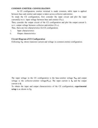
  • 1. COMMON EMITTER CONFIGURATION In CE configuration, emitter terminal is made common, while input is applied between base and emitter and output is taken across collector and emitter. To study the CE configuration, first consider the input circuit and plot the input current(IB) w.r.t. input voltage between base and emitter (VBE). Then, consider the output circuit of the CE configuration and plot the output current IC w.r.t. output voltage between collector and emitter (VCE). Thus, there are two characteristics for CE configuration. i. Input characteristics ii. Output characteristics Circuit Diagram of CE Configuration Following fig. shows transistor current and voltage in common emitter configuration. The input voltage in the CE configuration is the base-emitter voltage VBE and output voltage is the collector-emitter voltage(VCE). The input current is IB and the output current is IC. To obtain the input and output characteristics of the CE configuration, experimental setup is as shown in fig.
  • 2. Potentiometer R1 is used to vary the input current IB. To measure the current IB, milliammeter is connected series as shown. Similarly, to measure the collector Current IC, milliammeter is connected in series with potentiometer R2, in the output circuit. Input voltage VBE is measured using a DC voltmeter connected between the base and emitter. Output voltage VCE is measured using a DC voltmeter connected between collector and emitter. Input Characteristics for CE Configuration Input characteristics are plotted by considering only the input parameters i.e. input current IB and input voltage VBE. Input characteristics give the relationship between base current IB and base to emitter voltage VBE. To obtain the input characteristics of CE configuration, voltage between collector to emitter i.e. VCE is kept constant by adjusting the R2. Adjust VCE= 1V and keep it constant and then increase the voltage VBE in small suitable steps of in order of 0.1V and record the corresponding values of input current IB. Thus, we get the set of value of IB for different values of VBE, for VCE= 1V constant. Repeat the similar steps by keeping VCE= 5V to get the 2nd set of readings and finally by keeping VCE= 10V to get the 3rd set of readings. Each set of reading is plotted such that current IB is taken on Y-axis and the voltage VBE on X-axis. Thus, we get three curves for three different values of VCE as shown in the fig. From the input characteristics, we observe the following important points: 1. For region OA of the curve, the base current is very small. This voltage at which we get very small base current is called as cut-in voltage or knee voltage. It is denoted by Vk. The value of knee voltage is approximately 0.5 for silicon and 0.1V for germanium.
  • 3. 2. After the cut-in voltage (i.e. after the point A) the base current increases rapidly with small increase in the base to emitter voltage VBE. This indicates that the dynamic input resistance is small in CE configuration. 3. Dynamic resistance(ri) is given by the ratio of change in base-emitter voltage(VBE) to the resulting change in the base current(IB) at constant VCE. ri= 𝑉𝐵𝐸 𝐼𝐵 VCE= constant 4. For fixed value of VBE, IB decreases as VCE increases. The increase in VCE increases the reverse bias across the junction JC. This increases the depletion layer width across JC, this reduces the effective base width between JE and JC and due to this the overall base current reduces. Output Characteristics for CE Configuration Output characteristics is plotted by considering only the output parameters i.e. output current IC and output voltage between collector and emitter VCE. To obtain the output characteristic of CE configuration, the current IB is kept constant. To do this, vary R1 to adjust base-emitter voltage VBE, which set the suitable value of current IB(say 20A). Then increase the voltage VCE in suitable steps of order of 1V by using POT R2, then record the values of collector current IC corresponding to different values of VCE. Plot IC on ‘Y’ axis and VCE on ‘X’ axis. Repeat similar steps for values of IB as 40A, 60A etc. to get different curves as shown in fig. IC(MA). From the output characteristics we observe the following important points: 1. This characteristics shows relation between collector current IC and collector to emitter voltage VCE for fixed value of IB. This characteristic is also called as collector characteristic.
  • 4. 2. The output characteristic is divided into three important regions. i. Active region ii. Saturation region iii. Cutoff region 3. The value of dc of the transistor can be found at any point on the characteristics by taking the ratio IC to IB at that point. dc= Ic IB This is called as DC beta for the transistor. Similarly, if we take the ratio of change in IC i.e. IC to change in IB i.e. IB for a fixed value of VCE then it gives AC beta i.e. ac. ac= IC IB VCE= Constant Generally values of ac and dc are nearly equal. value is always greater than 1. 4. From the curve it is seen that the large change in VCE causes very small change in IC for constant IB. This indicates that the dynamic output resistance (r0) is high in CE configuration. r0= VCE Ic 5. Active region: The active region where the curves are approximately horizontal or flat is called as Active region. Increase in voltage VCE, increases the reverse bias across the junction JC. This increases the depletion layer width between JE and JC reduces. This reduces the base current IC. For this reason, CE output characteristics are sloping upwards. 6. Cutoff region: The collctor current IC is not zero, even when the base current IB is zero. Thus there exists a small value of collector current. This is called as reverse leakage current denoted by ICEO. Under this condition the transistor is said to be in cutoff state. 7. Saturation region: If VCE is reduced to a small value such as 0.2V then, the collector base junction JC gets forward biased and emitter base junction JE and JC is already forward biased. Thus, both the junctions JE gets forward biased. This rapidly increases the collector current IC. The region showing this is called as saturation region. In saturation region, we cannot keep control over the current IC. 8. In the active region: If we go on increasing the value of VCE beyond certain maximum value, then the breakdown occurs. This gives very high collector current. This effect is called as punch through effect.
  • 5. TRANSISTOR BIASING To operate the transistor exactly in the active region it is necessary to keep the base – emitter junction(JE) properly forward biased and collector base junction (JC) properly reverse biased, during application of input signal to the transistor. Doing this is called as biasing and the circuit designed to do this is called as biasing circuit. Thus biasing of transistor makes sure that the transistor is ON and remains in the active region where it operates linearly and provides a constant amount of voltage gain. Biasing sets up a fixed current through transistor (IB and IC), with a fixed voltage drop, across the transistor junctions (VBE and VCE). The proper values of these currents and voltages force the transistor to amplify the input weak signal faithfully. Biasing of transistor fixes the current IC and voltage VCE i.e. it fixes up a point on the output characteristics. This point is called as operating point of transistor, denoted by Q. It is also called as Quiescent Point. Conditions to be fulfilled during biasing the transistor are: 1. Transistor should work in active region and cannot enter in saturation or cutoff regions. 2. Transistor Q point should be at the central area of active region. 3. IC, IB, and VCE, VBE must be constant. DC Load Line (Also see class notes for other methods) The DC load line is the line on the output characteristics, which gives the values of IC and VCE for zero input signal i.e. DC conditions. To draw the DC load line, consider the following circuit as shown in fig.
  • 6. Here, VCC = ICRC + VCE=0  ICRC= VCC-VCE IC=- 1 Rc VCE+ VCC Rc Comparing this equation with the equation, y= mx +c Which is a straight line equation. We get, Slope (m) = - 1 𝑅𝑐 And ‘Y’- axis intercept is c = 𝑉𝑐𝑐 𝑅𝑐 Now plotting this line on the output characteristics of transistor, we get fig as shown below. The straight line on the output characteristics is called as DC load line. The two end points on the line are VCC (on X axis) and 𝑉𝑐𝑐 𝑅𝑐 (on Y-axis).
  • 7. These two points are located on the characteristics as follows: 1. When collector current IC = 0, VCE will be maximum and is given as VCE = VCC –ICRC VCE (Max) = VCC -0(RC) VCE (Max) = VCC Thus, we get one point on X-axis 2. When collector to emitter voltage VCE =0 then, IC will be maximum and it is given as: VCE = VCC- ICRC 0 = VCC –ICmax. RC  Icmax = 𝑉𝑐𝑐 𝑅𝑐 Thus we get one point on the Y-axis. Thus, connecting these two points, we get a DC load line. As shown in fig. DC load line gives us the following information: i. The DC load line intersects the horizontal (X) axis at point B. The point is called as transistor cutoff point. At this point, the values of base current IB and collector current IC are ideally zero. But practically small reverse saturation current flows (ICEO) and the voltage VCE is highly less than VCC. ii. The load line intersects the vertical Y-axis at point A. This point is called as transistor current is a maximum and the voltage VCE is very small equal to VCE(sat). The point where the DC load line cuts the output characteristics is called as the operating point Q as shown in fig. This Q point fixes up the current IC and voltage VCE, so that the transistor is continuously operated in the active region only. As Q point is shifted upwards, the transistor is operated near the saturation and when Q point is shift downwards then transistor is operated near cutoff and there is possibility that the transistor can turn off at any time. Thus, AC load line is drawn by considering values of IC and VCE when input AC voltage is applied to the transistor.
  • 8. Operating Point For operation of transistor in any application, fixed levels of currents IC, IB and voltages VCE, VBE are to be set. These values of currents and voltages define the point at which the transistor operates. This point is called as operating point. It is well ensured that the operating point must lie on the DC load line. Generally the operating point should lie at the center of the DC load line. The operating point is selected such that it should fulfill the following conditions:  The operating point is selected such that it should forward bias the base emitter junction(JE) and reverse bias the collector base junction (JC).  It should be such that, the transistor operates in the active region.  It should be such that the transistor should not be operated near cutoff or near saturation.  It should be such that the transistor will amplify the input signal magnitude without changing its wave shape. i.e. amplification without any distortion in the output.  Transistor gain should remain constant throughout its operation.