Electronics and Communication Engineering
•
0 likes•54 views

Electronics and Communication Engineering is the Branch of Engineering. Electronics and Communication Engineering field requires an understanding of core areas including Engineering Graphics, Computer Programming,Electronics Devices and Circuits-I, Network Analysis, Signals and Systems, Communication Systems, Electromagnetics Engineering, Digital Signal Processing, Embedded Systems, Microprocessor and Computer Architecture. Ekeeda offers Online Mechanical Engineering Courses for all the Subjects as per the Syllabus. Visit : https://ekeeda.com/streamdetails/stream/Electronics-and-Communication-Engineering

Recommended
More Related Content
What's hot
What's hot (20)
Similar to Electronics and Communication Engineering
Similar to Electronics and Communication Engineering (20)
More from Ekeeda
More from Ekeeda (20)
Recently uploaded
Recently uploaded (20)
Electronics and Communication Engineering
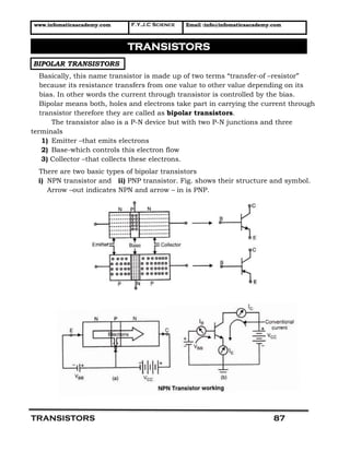
- 1. www.infomaticaacademy.com F.Y.J.C Science Email :info@infomaticaacademy.com TRANSISTORS 87 BIPOLAR TRANSISTORS Basically, this name transistor is made up of two terms “transfer-of –resistor” because its resistance transfers from one value to other value depending on its bias. In other words the current through transistor is controlled by the bias. Bipolar means both, holes and electrons take part in carrying the current through transistor therefore they are called as bipolar transistors. The transistor also is a P-N device but with two P-N junctions and three terminals 1) Emitter –that emits electrons 2) Base-which controls this electron flow 3) Collector –that collects these electrons. There are two basic types of bipolar transistors i) NPN transistor and ii) PNP transistor. Fig. shows their structure and symbol. Arrow –out indicates NPN and arrow – in is PNP. TRANSISTORS
- 2. www.infomaticaacademy.com F.Y.J.C Science Email :info@infomaticaacademy.com TRANSISTORS 88 Emitter – Base junction is forward biased and Base-Collector junction is reverse biased. In this method, transistor works as a controlled device. Refer the fig. it shows this biasing method. Base- Emitter is biased with low voltage batter BBV and Base – Collector with high voltage battery CCV . Now observe the battery connections, negative terminal of the battery BBV it will repel electrons towards the Base, they enter in the Base region. Base is P-type material and it is lightly doped thus few electrons recombine with holes and those number of electrons will pass into the Base towards positive terminal BBV . Rests of the electrons are attracted by positive terminal of the battery CCV through Collector. The Collector collects most of the electrons; therefore Emitter current is very close to the Collector current. E CI = I But as shown in the fig. we can say Emitter Current = Base current + Collector current E B CI I I Similarly fig. (b) shows the direction of conventional current from Collector to Emitter and fig. (a) shows the direction of electron flow. Alpha and Beta of Transistor The relation between Emitter current EI , and Collector current CI is given by alpha(α) and the relation between Base current BI and Collector current by β of the transistor. „β ‟ of a transistor tells us that small Base current controls a large Collector current.
- 3. www.infomaticaacademy.com F.Y.J.C Science Email :info@infomaticaacademy.com TRANSISTORS 89 C E C B Collector current Alpha α= Emitter current I α= …… I I Collector current Similarly Beeta β= Basecurrent I β= L II I Therelation between α and β is determined as follows E C B C C E E C E E B B E E B E I = I + I …… III I Sinceα= I =αI I Substituting I in equation III I =αI +I I = I -αI I = I 1-α C E B E C E B E Nowβis given by equation II and substituting I = αI and I = I 1-α I αI β= = I I 1-α α β= 1-α β Andit can beproved that α= 1+β C E B C E Example 1 : I = 98 mA, I = 100 mA and ,I = 2 mA then find α and β. Solution : I 98 α= = =0.98 I 100 That meansαisalwaysless than1 PNP TRANSISTOR The action of PNP transistor is quite similar to NPN transistor it differs in battery connection only. It requires opposite battery connections. Biasing method is same (FR), refer fig. (2.3) Emitter (P-type) is connected to positive terminal while Base (N-type) to negative and Collector (P-type) to negative terminal of high voltage battery CCV or Collector supply. Current through PNP transistor is due to holes as
- 4. www.infomaticaacademy.com F.Y.J.C Science Email :info@infomaticaacademy.com TRANSISTORS 90 it is due to electrons in NPN transistor. Compare the two diagrams fig. (2.2) and fig.(2.3) to understand the basic difference between biasing connections of NPN and PNP transistor and the direction of conventional current through the circuit. TRANSISTOR AMPLIFIER CONFIGURATIONS 1) Common Base Amplifier (CB) 2) Common Emitter Amplifier (CE) 3) Common Collector Amplifier (CC) 1) Common Base Amplifier In this type Base is common to both input and output. Output is taken from Collector. Observe the circuit, Input current is EI , output current is CI . C E E a) ,sinceI < I thecurrent gainin CBis<1. ) ,sinceI islarge;inputimpedanceof CBis verylow. ) C E in E Output Current I Currentgain Input Current I InputVoltage V b Input inpedance Input Current I OutputVoltag c Output impedance 0 C C V sinceI is verylarge;itislow I As input voltage increases and since Collector current is equal to Emitter current, it also increases (IC = IE). To develop a large output voltage, RC is m e Output Current 0 C C ade large so we get large output voltage.ItisV = I ×R
- 5. www.infomaticaacademy.com F.Y.J.C Science Email :info@infomaticaacademy.com TRANSISTORS 91 Similarly, as (AC) input when decreases at negative half cycle we get same change in the output. It is indicating that output is in phase with input. Since output resistance is large, we get amplified large output voltage. 2) Common Collector amplifier Here the Collector terminal is common to input and output. In common Collector configuration output is taken from Emitter therefore it is called as an „Emitter follower‟ and input is applied to the Base. Since CR is zero, Collector is directly connected to battery therefore it is a Collector grounded circuit because it is always at DC voltage or it is at AC ground. The Common Collector configuration is normally used as Emitter follower to get low output impedance. As shown in the fig. as input increases or decreases Base current varies and therefore Emitter current varies in the same manner. E B E B Output Current I a)Current gain = = =Veryhigh.SinceI isverysmallandI islarge Input Current I it'scurrent gainisveryhigh.
- 6. www.infomaticaacademy.com F.Y.J.C Science Email :info@infomaticaacademy.com TRANSISTORS 92 in B B Input Voltage V b)Inputimpedance = = ,sinceI is very small input impedance is very high. Input Current I 0 E E Output Voltage V c)Outputimpedance = = ,sinceI is very large it is low. Output Current I B B E C B E E E E V B B V The voltage gain of the amplifier is calculated as follows Suppose R = 10kΩ,I = 1 mA, I = 10 mA β=10 I =βI = I R =1K I ×R VoltageGain A = I ×R 10mA×1K = 1mA×10K 10 A = =1 10 Therefore the voltage gain of this amplifier is always 1 or less than one that means input and output are same in magnitude. The current gain of common Collector amplifier is large IE/IB but voltage gain is less than or equal to 1. The advantage of common Collector amplifier is its low output impedance and high input impedance. The output voltage is in phase with input. 3. Common Emitter Amplifier This configuration is most popular as an amplifier in almost all circuits, Emitter is grounded therefore it is called as grounded Emitter amplifier. In common Emitter amplifier input is applied through the Base and output is normally taken between Collector and ground. In common Emitter amplifier, we get large voltage gain but output voltage is 180⁰ out of phase with input voltage. We will discuss CE amplifier in detail later.
- 7. www.infomaticaacademy.com F.Y.J.C Science Email :info@infomaticaacademy.com TRANSISTORS 93 C C B B in B B Output Current I a) Current gain = = ,sinceI is verylargethan I it'scurrent gainishigh. Input Current I Input Voltage V b) Input impedance = = ,sinceI is verysmallitsinputimpedanceis veryhigh. Input Current I c)Outpu O C C Output Voltage V timpedance= = ,sinceI islargeitislow. Output Current I COMPARISON TRANSISTOR CHARACTERISTICS C CEI -V Characteristics of a transistor are one of the important characteristics it tells us how transistor behaves for different Base currents. Fig. shows the circuit diagram and these characteristic curves. CC CE B CC, C CE Where V =CollectorsupplyV = voltageacrossCollector,I =Basecurrent. By keeping the Base current constant and varying Collector supply V observation of Collector current I andV arenoted.These curves can be summarised as follows. i) When BI =0 Base current is zero, small Collector current flows this is because of minority current carriers in the Collector region. This is called as “reverse leakage current.” ii) In “active region” CI slowly increases with CEV . In active region the Collector current depends on the Base current and it is „β ‟ time larger than Base current. CB CC CE 1)Voltage Gain Low Less than or = 1 Maximum 2)Current Gain Less than 1 Very High Maximum 3)Input Impedance Lowest (=50 Ω) Highest (300KΩ) Medium (= 1KΩ) 4)Output Impedance Low Lowest (= 300Ω) Medium (= 50KΩ) 5) Phase inversion No No Yes (180⁰) 6) Application In RF Amplifier Emitter follower Amplifiers
- 8. www.infomaticaacademy.com F.Y.J.C Science Email :info@infomaticaacademy.com TRANSISTORS 94 iii) In „saturation region‟ the Collector current depends on the Base current and CEV is very small below 1 volt and in saturation, Base Collector diode becomes forward biased. a) The transistor is OFF in Cutoff region and current through transistor is zero. b) The transistor is ON in Active region and shows a linear change between BI and CI and CEV also between 0 and CCV . c) The transistor in Saturation is fully conducting current is maximum but CEV is almost zero. TRANSISTOR LOAD LINE The Common Emitter (CE) configuration is commonly used in amplifier circuit. Transistor with biasing resistor is shown in fig. as a common Emitter amplifier circuit. There are two resistors BR and CR or LR as Base bias resistor and Collector load resistor respectively. Proper biasing of transistor is very much important this is carried out by a load line analysis and calculations.
- 9. www.infomaticaacademy.com F.Y.J.C Science Email :info@infomaticaacademy.com TRANSISTORS 95 A load line is normally drawn on C CEI - V characteristics curves for the transistor used in amplifier circuit. When transistor is used as an amplifier two conditions must be verified. i) B-E junction must be forward biased and B-C junction reverse biased. ii) Transistor should not go into saturation and cutoff, it must be in active region. As shown in the fig. the first condition is satisfied but second condition is obtained by load line analysis and selecting the operating point „Q‟ The load line is drawn by taking two extreme conditions in to consideration as follows a) Saturation – At this point Collector current CI is maximum it is calculated by equation CE CC C L CC CC C(sat) CE CC L CC CC L L V = V - I R V V Put I = V = V - R =V -V =0 R R CC L CC C(sat) CE L V Thus Co-ordinates at saturation are (0, ) R V 12V For the circuit shown in the fig. I = = =12mAand V is zero (0.12mA) R 1K C CE CC C L CE CC CC CC, CE C CC CC L ) – At this point put I = 0 in equation V = V - I R V = V -0=V ThusCo-ordinateat cutoff is V 0 Thus we get two points V ,I V 1)A 0, 2)B(V ,0) R Refer the calculations for given circu b Cutoff it shown left side of the fig. (2.10) it is A (0, 12mA) and B(12V,0) Now after drawing a load line between these two points an operating point „Q‟ is located at the center of the load line, refer fig. At operating point „Q‟ we get a fixed DC Base current when input (AC) signal is zero. When AC signal varies, Base current varies above and below this operating point.
- 10. www.infomaticaacademy.com F.Y.J.C Science Email :info@infomaticaacademy.com TRANSISTORS 96 Effect of Q point Fig. shows the effect of incorrect biasing (incorrect position of Q point) and it shows what happens to the output signal if operating point is not properly selected. If „Q‟ point is not correct then we get distorted output which is undesired. As shown in fig. (a) and (b) where operating point is near cut off or saturation. Transistor goes into cut off and saturation, which produces distorted output. When it is near the center the output signal is undistorted as shown in fig. (c) BIASING METHODS Method I) Fixed Bias In this method as shown in fig. (a) two separate batteries BBV (low voltage) and CCV (high voltage) are connected through BR and CR resistors to get Base current BI and Collector current C BI = β× I . But instead of connecting two separate batteries we can take only battery CCV and by connecting a high value of resistor BR we can get low voltage as Base bias voltage refer fig. (b)
- 11. www.infomaticaacademy.com F.Y.J.C Science Email :info@infomaticaacademy.com TRANSISTORS 97 Method II) Collector – Base bias (Self Bias) This is a modified method from fixed bias circuit. Here Base bias is taken from Collector instead of CCV as shown in fig (a). Now when temperature increases the collector current increases due to increase in leakage current. But Collector voltage CEV decreases because more drop takes place across CR . Therefore Base bias voltage decreases; which reduces the Base current. Thus ultimately Collector current is maintained constant. This feedback from Collector to Base and this action is shown in fig (a), shows increase and shows decrease. C CE CE CC C C B B C C1) When temp , 2) I , 3) V (V = V - I R ), 4) V , 5) I , 6) I ; thus I is maintained. Method III) Emitter feedback Bias As shown in fig (2.13b) Emitter resistor ER is introduced to develop voltage across it to control Base current. When temperature increases, Collector current as well as
- 12. www.infomaticaacademy.com F.Y.J.C Science Email :info@infomaticaacademy.com TRANSISTORS 98 Emitter current EI increases which increases Emitter voltage EV and thus BEV Base to Emitter potential difference decreases. As BEV decreases Base current gets reduced as well as collector current. Thus voltage across Emitter resistor ER is used to get negative feedback, this circuit is known as Emitter feedback bias. Method IV) Voltage Divider – Bias (Stabilized Bias) This method is most popular in amplifier circuits because stabilization of Q point and temperature effect both are controlled. Here 1R and 2R are used to get Base biasing voltage divider type circuit. Similarly a capacitor across EC is shown in fig (a) Since 1 2R R form a voltage divider from CCV it is called as voltage divider bias. When temperature increases Collector current increases and since C EI = I Emitter current also increases. This EI flows through ER it increases voltage drop across ER i.e. E EI R but BE B EV =V -V therefore BEV gets reduced. This lowers the Base current. Thus increase in unwanted current is compensated; this sequence of operation is shown in fig (b). Similarly to avoid AC feedback a Emitter bypass capacitor is connected across ER to bypass AC voltage hence EC is known as emitter bypass capacitor. If there is no EC it would produce AC voltage and reduce the voltage gain. UNIPOLAR TRANSISTORS As we have studied transistors were bipolar transistors since their current carriers were both electrons and holes hence called bipolar.
- 13. www.infomaticaacademy.com F.Y.J.C Science Email :info@infomaticaacademy.com TRANSISTORS 99 i) FET (Field – Effect – Transistor) This type of transistor is called as unipolar device only one type of carriers either electrons or holes take part in carrying the currents. Bipolar transistor like NPN is operated with Base current but in case of FET, it is operated with gate voltage. It has three terminals. 1) Source just like Emitter 2) Drain like Collector 3) Gate like Base of bipolar transistor Below Fig. shows its construction, symbol and both types N-channel and P- channel. Since there is a junction it is known as junction field effect transistor or JFET. They are manufactured in two types N-channel JFET and P-channel JFET. N-channel JFET has a N-bar in which two P-regions are attached to form a gate terminal. Here source terminal acts as a source of electrons. Gate, which controls this flow through N-channel from terminal source to drain. Drain is normally connected to high positive voltage called as DDV , it drains electrons. The gate voltage is normally in reverse bias with respect to source called as GSV . I-V Characteristics of FET (Operation) Let us see how FET controls the drain current DI by gate voltages GSV . Fig. shows the circuit diagram and curves of DI verses DSV for different values of GSV .
- 14. www.infomaticaacademy.com F.Y.J.C Science Email :info@infomaticaacademy.com TRANSISTORS 100 Refer fig (a) current flows (conventional) from drain to source but electrons are attracted by drain voltage DDV . This electron flows is opposed by reverse bias gate voltage because of reverse voltage, opposing field or a depletion region is developed therefore small number of electrons flow from source to drain. Fig. (b) shows if GSV is more negative then N channel becomes very narrow which stops electron flow this is called as „Pinch – off region‟. The I-V characteristic shows, as GSV voltage becomes more and more negative drain current becomes low. After particular drain voltage, JFET goes into breakdown and then current suddenly increases to a high value. In case of JFET Gate current is almost zero hence it is called as a voltage operated device. It has very high input impedance since gate current is zero, practically a small leakage current flows. ii)MOSFET (Metal Oxide Semiconductor FET) In junction FET due to leakage current small gate current floes; that can be reduced by insulating gate from channel by using insulating material silicon dioxide therefore it is called „Metal-Oxide Semiconductor‟ or MOSFET sometimes MOSFETs are called as „IGFET‟ Insulated gate FET. MOSFET can be of two types: i) Depletion type MOSFET (N-channel and P-channel) ii) Enhancement type MOSFET (N-channel and P-channel) Fig. illustrates the structure and symbol of depletion MOSFET in both types N- channel and P-channel.
- 15. www.infomaticaacademy.com F.Y.J.C Science Email :info@infomaticaacademy.com TRANSISTORS 101 MOSFET has four terminals drain, source, insulated Gate with Silicon dioxide and a substrate. Normally substrate is connected to the source as it is shown in symbol. Arrow “IN” indicates N-channel and arrow “OUT” indicates P-channel MOSFET. In enhancement MOSFET construction is different as it is shown by fig. there is a region between source and drain. P-substrate separates these two N-regions. Operation MOSFET is operated with gate voltage ( GSV ), when GSV is zero or negative then in case of N-channel MOSFET, it is cut off because there is a P-region in between drain and source. But when GSV is made sufficient positive called as threshold voltage a N-type inversion layer connects source to drain, current flows through this layer. Due to silicon dioxide insulator, gate – SiO2 – P – region form a capacitance as shown in fig. When positive voltage is applied to the gate, electrons can be accumulated on other side as shown with N-layer.
- 16. www.infomaticaacademy.com F.Y.J.C Science Email :info@infomaticaacademy.com TRANSISTORS 102 Thus, more is the GSV positive more will be the width of N-inversion layer and therefore more electrons can flow from source to drain. Since insulator is connected in gate circuit gate current is almost zero. This indicates that MOSFET has very high input impedance. MOSFET‟s are used in microprocessors as an electronic switch. Because of very small gate current, power required for MOSFET is very small it can be operated with small button cell. By connecting complementary MOSFET (P-channel) with (N-channel) MOSFET a new type of circuit is formed called as “CMOS” Complementary MOSFET. Fig. shows the I-V Characteristics of MOSFET. Drain current depends on DDV and GSV . (A load line can be drawn similar to transistor between DD D V R instead of CC L V R and DDV instead of CCV of bipolar transistor. iii) Uni-Junction Transistor (UJT) UJT is a special type of unipolar transistor usually used a s an electronic switch. It has two doped regions and three terminals BASE1, BASE2 and EMITTER. Refer the fig. (a), it shows its structure and symbol. The emitter is heavily doped and base is lightly doped. Since the device has one P-N junction and three leads, it is commonly known as Uni-junction transistor (Uni means single). Fig. (b) shows the equivalent circuit of a UJT. The resistance of the silicon bar is called as inter-base resistance BBR . Two resistors in series represent the inter – base resistance viz.
- 17. www.infomaticaacademy.com F.Y.J.C Science Email :info@infomaticaacademy.com TRANSISTORS 103 a) B2R is the resistance of silicon bar between 2B and the point at which the emitter junction lies. b) B1R is the resistance of the bar between 1B and emitter junction. This resistance is shown variable because its value depends upon the bias voltage across the P-N junction. The P-N junction is represented in the emitter by a diode D. The circuit action of a UJT can be easily explained from its equivalent circuit. i) with no voltage applied to the UJT, the inter-base resistance is given by; BB B1 B2R = R + R The value of BBR generally lies between 4 K Ω and 10KΩ ii) If a voltage BBV is applied between the bases with emitter open, the voltage will divide up across B1R and B2R . B1 B1, RB1 BB B1 B2 B1 RB1 BB B1 B2 R Voltage across R V = V R +R R Or V /V = R +R The ratio RB1 BBV /V is called intrinsic stand – off ratio and is represented by letter η. Characteristics of UJT
- 18. www.infomaticaacademy.com F.Y.J.C Science Email :info@infomaticaacademy.com TRANSISTORS 104 Fig. shows E EI -V characteristic curve. Initially, when the UJT is in cut-off as we increase from zero, very small current flows from terminal B2 to the emitter. This is known as leakage current. Above a certain value of EV forward emitter current starts increasing till EV reaches to peak point. After the peak point current through UJT suddenly increases and EV decreases to a very low point. This part of curve is known as negative resistance characteristics of UJT. When EI increases to a very low point known as valley point the device goes into saturation. SOLVED PROBLEMS 1) In a transistor characteristics Base current is 100μA , Calculate EI , CI , if β = 100. B C B C E B C Solution : I = 100μA, I = β×I = 100 × 100μA I =100×0.1mA 100μA=0.1mA =10mA Now Emitter current =I =I +I =0.1mA+10mA =10.1mA 2) If α of a transistor is 0.95 find β α 0.95 0.95 Solution: β 19 1 α 1 0.95 0.05
- 19. www.infomaticaacademy.com F.Y.J.C Science Email :info@infomaticaacademy.com TRANSISTORS 105 3) In a transistor characteristics base current is 100μ A, if β of the transistor is 100 calculate CI and EI and CEV if CCV = 24V and CR = 1K B C B C B E C B CE CC C C Solution: Given I = 100μA = 0.1mA a) Since β = I /I I = β × I =100×0.1mA = 10mA b) Now I = I + I = 10mA+0.1mA=10.1mA c) V =V -I R =24- 10 10-3 1 103 24 10 14 .V 4) A UJT has supply of 12 volts find peak emitter voltage if it‟s B1R is 6 KΩ and B2R is 4KΩ B1 B2BB B1 B1 B2 EP BB D Solution: V =12V, R = 6KΩ R =4KΩ R 6K η = = =0.6 R +R 10K V =ηV +V =7.2+0.7=7.9 Volt