
Recommended
Recommended
More Related Content
Similar to Original N-Channel Mosfet CS13N50 13N50 500V 13A TO-220 New
Similar to Original N-Channel Mosfet CS13N50 13N50 500V 13A TO-220 New (20)
More from AUTHELECTRONIC
More from AUTHELECTRONIC (20)
Recently uploaded
Recently uploaded (20)
Original N-Channel Mosfet CS13N50 13N50 500V 13A TO-220 New
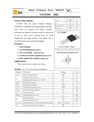
- 1. CS13N50 A8H WUXI CHINA RESOURCES HUAJING MICROELECTRONICS CO., LTD. Page 1 of 10 2015V01 ○R Silicon N-Channel Power MOSFET General Description: CS13N50 A8H, the silicon N-channel Enhanced VDMOSFETs, is obtained by the self-aligned planar Technology which reduce the conduction loss, improve switching performance and enhance the avalanche energy. The transistor can be used in various power switching circuit for system miniaturization and higher efficiency. The package form is TO-220AB, which accords with the RoHS standard. Features: l Fast Switching l Low ON Resistance(Rdson≤0.45Ω) l Low Gate Charge (Typical Data:45nC) l Low Reverse transfer capacitances(Typical:23pF) l 100% Single Pulse avalanche energy Test Applications: Power switch circuit of adaptor and charger. Absolute(Tc= 25 unless otherwise specified℃ ): Symbol Parameter Rating Units VDSS Drain-to-Source Voltage 500 V ID Continuous Drain Current 13 A Continuous Drain Current TC = 100 °C 10 A IDM a1 Pulsed Drain Current 52 A VGS Gate-to-Source Voltage ±30 V EAS a2 Single Pulse Avalanche Energy 1100 mJ EAR a1 Avalanche Energy ,Repetitive 78 mJ IAR a1 Avalanche Current 4.0 A dv/dt a3 Peak Diode Recovery dv/dt 5 V/ns PD Power Dissipation 150 W Derating Factor above 25°C 1.2 W/℃ TJ,Tstg Operating Junction and Storage Temperature Range 150,–55 to 150 ℃ TL Maximum Temperature for Soldering 300 ℃ VDSS 500 V ID 13 A PD (TC=25℃) 150 W RDS(ON)Typ 0.34 Ω
- 2. CS13N50 A8H ○R WUXI CHINA RESOURCES HUAJING MICROELECTRONICS CO., LTD. Page 2 of 10 2015V01 Electrical Characteristics(Tc= 25 unless otherwise specified℃ ): OFF Characteristics Symbol Parameter Test Conditions Rating Units Min. Typ. Max. VDSS Drain to Source Breakdown Voltage VGS=0V, ID=250µA 500 -- -- V ΔBVDSS/ΔTJ Bvdss Temperature Coefficient ID=250uA,Reference25℃ -- 0.54 -- V/℃ IDSS Drain to Source Leakage Current VDS =500V, VGS= 0V, Ta = 25℃ -- -- 1 µAVDS =400V, VGS= 0V, Ta = 125℃ -- -- 100 IGSS(F) Gate to Source Forward Leakage VGS =+30V -- -- 100 nA IGSS(R) Gate to Source Reverse Leakage VGS =-30V -- -- -100 nA ON Characteristics Symbol Parameter Test Conditions Rating Units Min. Typ. Max. RDS(ON) Drain-to-Source On-Resistance VGS=10V,ID=6.5A -- 0.34 0.45 Ω VGS(TH) Gate Threshold Voltage VDS = VGS, ID = 250µA 2.0 4.0 V Pulse width tp≤300µs,δ≤2% Dynamic Characteristics Symbol Parameter Test Conditions Rating Units Min. Typ. Max. gfs Forward Transconductance VDS=15V, ID =6.5A -- 12 -- S Ciss Input Capacitance VGS = 0V VDS = 25V f = 1.0MHz -- 2130 -- pFCoss Output Capacitance -- 210 -- Crss Reverse Transfer Capacitance -- 23 -- Resistive Switching Characteristics Symbol Parameter Test Conditions Rating Units Min. Typ. Max. td(ON) Turn-on Delay Time ID =13A VDD =250V VGS = 10V RG =6.1Ω -- 14 -- ns tr Rise Time -- 27 -- td(OFF) Turn-Off Delay Time -- 45 -- tf Fall Time -- 36 -- Qg Total Gate Charge ID =13A VDD =250V VGS = 10V -- 45 nCQgs Gate to Source Charge -- 10 -- Qgd Gate to Drain (“Miller”)Charge -- 18 --
- 3. CS13N50 A8H ○R WUXI CHINA RESOURCES HUAJING MICROELECTRONICS CO., LTD. Page 3 of 10 2015V01 Source-Drain Diode Characteristics Symbol Parameter Test Conditions Rating Units Min. Typ. Max. IS Continuous Source Current (Body Diode) -- -- 13 A ISM Maximum Pulsed Current (Body Diode) -- -- 52 A VSD Diode Forward Voltage IS=13A,VGS=0V -- -- 1.5 V trr Reverse Recovery Time IS=13.0A,Tj =150°C dIF/dt=100A/us, -- 506 -- ns Qrr Reverse Recovery Charge -- 4.2 µC Pulse width tp≤300µs,δ≤2% Symbol Parameter Typ. Units RθJC Junction-to-Case 0.83 /W℃ RθJA Junction-to-Ambient 62 /W℃ a1 :Repetitive rating; pulse width limited by maximum junction temperature a2 :L=6.5mH, ID=14.8A, Start TJ=25℃ a3 :ISD =13A,di/dt ≤100A/us,VDD≤BVDS, Start TJ=25℃
- 4. CS13N50 A8H ○R WUXI CHINA RESOURCES HUAJING MICROELECTRONICS CO., LTD. Page 4 of 10 2015V01 Vds,Drain Source Voltage,Volts Id,DrainCurrent,Amps 1 0.01 0.1 10 1 10 100 100 1000 Characteristics Curve: 0.01 0.1 1 0.00001 0.0001 0.001 0.01 0.1 1 Rectangular Pulse Duration,Seconds ThermalImpedance,Normalized Vds , Drain-to-Source Voltage , Volts 0 0 3 5 10 15 Id,DrainCurrent,Amps 6 9 12 15 20 25 30 35 21 18 Figure 2 Maximum Power Dissipation vs Case Temperature Figure 5 Maximum Effective Thermal Impendance , Junction to Case Figure 4 Typical Output CharacteristicsFigure 3 Maximum Continuous Drain Current vs Case Temperature Figure 1 Maximum Forward Bias Safe OperatingArea DC 1ms 10ms VGS=9V VGS=5V VGS=6V VGS=7V VGS=8V PDM t2 t1 NOTES: DUTY FACTOR :D=t1/ t2 PEAKTj=PDM*ZthJC*RthJC+TC 50% 20% 10% 5% Single pulse 2% 1% 100μs 50 Tc , Case Tem perature , C 80 Pd,PowerDissipation,Watts 0 0 40 25 120 160 200 10075 125 150 Tc , Case Temperature ,C 6 Id,DrainCurrent,Amps 25 0 3 50 15 9 12 75 100 125 1500 18 OPERATION IN THISAREA MAY BE LIMITED BY RDS(ON) TJ=MAX RATED TC=25℃ Single Pulse
- 5. CS13N50 A8H ○R WUXI CHINA RESOURCES HUAJING MICROELECTRONICS CO., LTD. Page 5 of 10 2015V01 Rds(on),DraintoSourceON Resistance,Ohms ,Vgs , Gate to Source Voltage 4 0 6 8 10 Volts 12 14 0.25 0.75 1 1.25 1.5 0.5 -100 -50 0 50 100 150 200 Tj, Junction temperature ,C Rds(on),DraintoSourceON Resistance,Nomalized 0 0.5 1 1.5 2 2.5 3 Id , Drain Current , Amps Resistance,Ohms Rds(on),DraintoSourceON 0 10 20 30 40 50 60 0.3 0.4 0.5 0.6 0.7 0.8 Vgs , Gate to Source Voltage , Volts Id,DrainCurrent,Amps 0 0 14 12 10 8 6 4 2 1 2 3 4 5 6 Idm,PeakCurrent,Amps 1.00E-011.00E-05 1 10 1.00E-04 1.00E-03 1.00E-02 Pulse Width , Secondst 1.00E+00 100 1.00E+01 Figure 6 Maximun Peak Current Capability Figure 8 Typical Drain to Source ON Resistance vs Gate Voltage and Drain Current Figure 7 Typical Transfer Characteristics Figure 10 Typical Drian to Source on Resistance vs Junction Temperature Figure 9 Typical Drain to Source ON Resistance vs Drain Current TRANSCONDUCTANCE MAY LIMIT CURRENT IN THIS REGION FOR TEMPERATURES ABOVE 25℃ DERATE PEAK CURRENT AS FOLLOWS: − = 125 150 25 CT II ID= 13A ID= 6.5A ID= 3.25A VGS=10V PULSE DURATION = 10μs DUTY FACTOR = 0.5%MAX Tc =25 ℃ PULSED TEST VDS=30V PULSED TEST Tc =25 ℃ PULSED TEST VGS=10V ID=6.5A VGS=10V
- 6. CS13N50 A8H ○R WUXI CHINA RESOURCES HUAJING MICROELECTRONICS CO., LTD. Page 6 of 10 2015V01 BreakdownVoltage,Normalized 0.9 -75 Tj, Junction temperature , C 25-25-50 0 50 10075 150125 175 Bvdss,DraintoSource 0.95 1 1.05 1.1 1.15 0 1 2 3 4 5 6 0.4 0.5 0.6 0.7 0.8 0.9 1 1.1 Vsd , Source - Drain Voltage , Volts Isd,ReverseDrainCurrent,Amps 25 Vgs,GatetoSourceVoltage,Volts 0 0 3 9 6 12 15 100 Qg , Total Gate Charge , nC 50 75 125 Vds , Drain - Source Voltage , Volts 100 20 Capacitance,pF 30 40 50 60 4000 6000 8000 10000 2000 0 0.7 0.8 0.9 1 1.1 1.2 -100 -50 0 50 100 150 200 Tj, Junction temperature , C Vgs(th),ThresholdVoltage,Nomalized Figure 13 Typical Capacitance vs Drain to Source Voltage Figure 16 Unclamped Inductive Switching CapabilityFigure 15 Typical Body Diode Transfer Characteristics Figure 14 Typical Gate Charge vs Gate to Source Voltage tav , Time in Avalanche , Seconds 1.00E-06 0.1 1.00E-05 10 Id,DrainCurrent,Amps 1 100 1.00E-04 1.00E-03 1.00E-02 1.00E-01 Ciss Coss Crss VGS=0V , f=1MHz Ciss=Cgs+Cgd Coss=Cds+Cgd Crss=Cgd VDS=400V ID=13A +150℃ +25℃ -55℃ STARTING Tj = 25℃ STARTING Tj = 150℃ If R=0: tAV=(L* IAS) / (1.38VDSS-VDD) If R≠0: tAV=(L/R) In[IAS*R/ (1.38VDSS-VDD)+1] R equals total Series resistance of Drain circuit Figure 11 Typical Theshold Voltage vs Junction Temperature Figure 12 Typical Breakdown Voltage vs Junction Temperature VGS=0V ID=250μA VGS=0V ID=250μA VGS=0V
- 7. CS13N50 A8H ○R WUXI CHINA RESOURCES HUAJING MICROELECTRONICS CO., LTD. Page 7 of 10 2015V01 Test Circuit and Waveform
- 8. CS13N50 A8H ○R WUXI CHINA RESOURCES HUAJING MICROELECTRONICS CO., LTD. Page 8 of 10 2015V01
- 9. CS13N50 A8H ○R WUXI CHINA RESOURCES HUAJING MICROELECTRONICS CO., LTD. Page 9 of 10 2015V01 Package Information: TO-220AB Package Items Values(mm) MIN MAX A 10.00 10.60 B 15.0 16.0 B1 8.90 9.50 C 4.30 4.80 C1 2.30 3.10 D 1.20 1.40 E 0.70 0.90 F 0.30 0.60 G 1.17 1.37 H 3.30 3.80 L 12.7 14.7 N 2.34 2.74 Q 2.40 3.00 3.50 3.90
- 10. CS13N50 A8H ○R WUXI CHINA RESOURCES HUAJING MICROELECTRONICS CO., LTD. Page 10 of 10 2015V01 The name and content of poisonous and harmful material in products Part’s Name Hazardous Substance Pb Hg Cd Cr(VI) PBB PBDE Limit ≤0.1% ≤0.1% ≤0.01% ≤0.1% ≤0.1% ≤0.1% Lead Frame ○ ○ ○ ○ ○ ○ Molding Compound ○ ○ ○ ○ ○ ○ Chip ○ ○ ○ ○ ○ ○ Wire Bonding ○ ○ ○ ○ ○ ○ Solder × ○ ○ ○ ○ ○ Note ○:means the hazardous material is under the criterion of SJ/T11363-2006. ×:means the hazardous material exceeds the criterion of SJ/T11363-2006. The plumbum element of solder exist in products presently, but within the allowed range of Eurogroup’s RoHS. Warnings 1. Exceeding the maximum ratings of the device in performance may cause damage to the device, even the permanent failure, which may affect the dependability of the machine. It is suggested to be used under 80 percent of the maximum ratings of the device. 2. When installing the heatsink, please pay attention to the torsional moment and the smoothness of the heatsink. 3. VDMOSFETs is the device which is sensitive to the static electricity, it is necessary to protect the device from being damaged by the static electricity when using it. 4. This publication is made by Huajing Microelectronics and subject to regular change without notice. WUXI CHINA RESOURCES HUAJING MICROELECTRONICS CO., LTD. Add: No.14 Liangxi RD. Wuxi, Jiangsu, China Mail:214061 HTUhttp://www. crhj.com.cnUTH Tel: +86 0510-85807228 Fax: +86- 0510-85800864 Marketing Part: Post:214061 Tel: +86 0510-81805277/81805336 Fax: +86 0510-85800360/85803016 E-mail:sales@hj.crmicro.com Application and Service:Post:214061 Tel / Fax:+86- 0510-81805243/81805110