International Journal of Engineering Inventions (IJEI)
•
0 likes•267 views

www.ijeijournal.com
![Demodulation of Differential Binaryphase Shift…
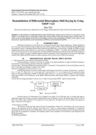
Synchronous To integrate and
b (t) √2Ps cos(ω0t+θ) Demodulator Synchronizer
(Multiper)
ω0Tb=2nπ Delay Tb
b(t-Tb) )√2Ps cos [ω0(t-Tb)+θ]
Fig 2 Demodulation of DPSK signal
III. IMPLEMENTATION
The bit synchronizer portion of the STEL-2110A chip, is a digital phase locked loop which operates by integrating
the input signals in the both the I and Q channels over one symbol period. This is done three times. The difference between
the last two gives an indication of the timing error, since the averaged difference will be zero when the timing is correct. This
signal is used to drive a numerically controlled oscillator (NCO) which produces the clock signals to drive the entire circuit
as well as sampling the incoming signals. The signals can also be integrated prior to the main timing integrators. This can
simplify operation over a wide range of data rates by maintaining a constant sampling rate, thereby eliminating the need to
change the filter before the A/D converters. The number of accumulation per symbol in this section is controlled by the pre-
accumulation control factor Ai. This pre-accumulation factor can be to one, two, four, eight or sixteen times. The optimally
integrated IOPT and QOPT signals are used to drive a DPSK output and a feedback signal to control the local oscillator for
carrier tracking.
The signal can be selected to be phase locked loop (PLL) control signal or an automatic frequency control (AFC)
signal. The former is intended for coherent demodulation in continuous carrier systems, when the IOPT and QOPT signals will
be the data outputs, and the latter is intended for use where fast acquisition is required, e.g., in burst carrier systems, such as
TDMA, where the acquisition time of a PLL would case significant loss of a data at the beginning of each burst. In such case
either differential demodulation should be used or a STEL-2210 Block Phase Estimation can be used to compensate for the
residual phase roll in burst application. An output signal derived from the I and Q data can be processed to give an indication
of when the timing recovery circuit in lock. A.
A. Function Block Description
Following blocks are used to develop the logic of Demodulation of DPSK
I and Q Channel Integration Block
Timing Discriminator Block
Timing Generation Block
Bit Timing NCO Block
Simulation Software and Code example
Lock Detector Block
Carrier Discriminator Block
B. I and Q Channel Integration Block
The I and Q channel integrator block consists of two major sub-blocks: the pre-accumulators allow the signal to be
integrated over 1 to 16 samples according to the setting of the pre-accumulation factor, Ai. Increasing the value of Ai gives a
larger number of samples per symbol and allows the sampling rate to be maintained within a narrow range while the data
rate varies over a wide range. The signal levels are automatically
integrators. In this section there are three accumulators in each channel, for early, late and punctual integrations of
the signal. The number of accumulation per symbol in this section can be
of samples are integrated in each symbol period. The outputs of pre-accumulators are fed into the main I and Q channel.
In this section there are three accumulators in each channel, for early, late and punctual integrations of the signal. The
number of accumulation per symbol in this section can be either four or eight, according to the setting of the control
parameter, Ss, so that the total number of input samples per symbol is then Ss x Ai.
C. Timing Discriminator Block
The difference between the Early and Late integration provide the discriminator function for the bit synchronizer
function. The differential output from the I and Q channels are then summed and passed into the loop filter block. The
individual I and Q channel components in the discriminator can also be disabled by means of the signal ICDD and QCDD.
This allows the noise in these channels to be eliminated when receiving a BPSK signal once lock has been achieved.
Demodulation is then coherent and the signal is all in one channel. The punctual integrations are then the optimal I and Q
signal for each symbol. The combined discriminator signal is also available at pins BSD8-0.
D. Timing Generator Block
The timing generator block generates all the timing signals used internally from either numerically controlled
oscillator NCO output or the ESCK signal. The input signal to the timing generator block is also the converter clock (CVCK)
signal
ISSN: 2278-7461 www.ijeijournal.com P a g e | 28](data:image/gif;base64,R0lGODlhAQABAIAAAAAAAP///yH5BAEAAAAALAAAAAABAAEAAAIBRAA7)
Recommended
Recommended
More Related Content
What's hot
What's hot (20)
Viewers also liked
Viewers also liked (7)
Similar to International Journal of Engineering Inventions (IJEI)
Similar to International Journal of Engineering Inventions (IJEI) (20)
More from International Journal of Engineering Inventions www.ijeijournal.com
International Journal of Engineering Inventions (IJEI)
- 1. International Journal of Engineering Inventions ISSN: 2278-7461, www.ijeijournal.com Volume 1, Issue 9 (November2012) PP: 27-31 Demodulation of Differential Binaryphase Shift Keying by Using VDSP++4.5 Ittee Teli Electrical and Electronics Department G.B.P.Engg.College Ghurdori Pauri Garhwal Uttrakhand, India Abstract:––In Demodulation of Differential Binary Phase Shift Keying, Timing recovery Process is to be done by using VDSP++ 4.5 software tools, by using STEL-2110A Chip Circuitry. STEL 2110A chip circuitry have a software base , in which we have a block diagram on the help of this diagram we find out the demodulation of DPSK .In this paper we are discussed on digital modulation and the demodulation of DPSK is more beneficial than BPSK . I. INTRODUCTION Modulation techniques are of two types, one is Analog and another one is Digital modulations. Digital modulations are of two type-coherent and non-coherent detection. The coherent version of PSK is Binary Phase Shift Keying (BPSK) and non-coherent version is Differential Binary Phase Shift Keying (DPSK).Due to shortcoming of BPSK the DPSK has been introduced and widely used and hence it is also known as modification of BPSK. To analyze the Demodulation of DPSK STEL-2110A chip circuitry is used, which has Bit synchronizer/PSK Demodulator provides bit timing control the sampling of the signal in a receiver as well as a feedback signal to control the frequency of the local oscillator It can be used in high speed coherent PSK, QPSK and DPSK modems in either continuous carrier or burst carrier (TDMA) environments. II. DIFFERENTIAL BINARY PHASE SHIFT KEYING A Differentail Binary Phase Shift Keying Modulation(DPSK) Analog modulation is sensitive to the noise as compare to the digital modulation .In digital modulation techniques, non-coherent is more used than coherent to reduce the complexity. In binary phase- shift keying (BPSK) the transmitted signal is a sinusoid of fixed amplitude .It has one fixed phase when the data is at the other level the phase is different 180 º.If the sinusoid is of amplitude A it has a power Ps =1/2 A2. In BPSK the data b(t) is a stream of binary digits with voltage levels which as a matter of convenience , we take to be at +1V and -1V .When b(t) =1V it is at logic level 1 and when b(t) =-1V it is at logic level 0. By squaring the input signals we get the demodulation of BPSK so that both signals become (+) ve and we face the problem of recognizing the input signal .DPSK is the modification of the BPSK. Differential phase shift keying (DPSK), a common form of phase modulation conveys data by changing the phase of carrier wave. A means for generating a DPSK signal is shown in Fig1 d (t) X-OR Balanced Modulator Delay Tb b (t-Tb) Fig 1 Generation of DPSK The data stream to be transmitted, d (t), is applied to one input of an X–OR logic gate. To another gate input is applied the output of the exclusive or gate b (t) delayed by the time Tb allocate to one bit. This second input is then b (t-Tb). In Fig we have drawn logic waveforms to the response b (t) to an input d (t). The upper level of the waveforms corresponds to logic 1, the lower level to logic 0. B. Demodaultion of DPSK The recovery of the base band signal is known as demodulation. When d (t) =0 the phase of the carrier does not change at the beginning of the bit interval, while when d (t) =1 there is a phase change of magnitude π. A method of recovering the data bit stream from the DPSK signal is shown in Fig2.Here the received signal and received signal delayed by the bit time Tb are applied to a multiplier. The multiplier output is and is applied to a bit synchronizer and integrator for the BPSK demodulator. the BPSK demodulator. ISSN: 2278-7461 www.ijeijournal.com P a g e | 27
- 2. Demodulation of Differential Binaryphase Shift… Synchronous To integrate and b (t) √2Ps cos(ω0t+θ) Demodulator Synchronizer (Multiper) ω0Tb=2nπ Delay Tb b(t-Tb) )√2Ps cos [ω0(t-Tb)+θ] Fig 2 Demodulation of DPSK signal III. IMPLEMENTATION The bit synchronizer portion of the STEL-2110A chip, is a digital phase locked loop which operates by integrating the input signals in the both the I and Q channels over one symbol period. This is done three times. The difference between the last two gives an indication of the timing error, since the averaged difference will be zero when the timing is correct. This signal is used to drive a numerically controlled oscillator (NCO) which produces the clock signals to drive the entire circuit as well as sampling the incoming signals. The signals can also be integrated prior to the main timing integrators. This can simplify operation over a wide range of data rates by maintaining a constant sampling rate, thereby eliminating the need to change the filter before the A/D converters. The number of accumulation per symbol in this section is controlled by the pre- accumulation control factor Ai. This pre-accumulation factor can be to one, two, four, eight or sixteen times. The optimally integrated IOPT and QOPT signals are used to drive a DPSK output and a feedback signal to control the local oscillator for carrier tracking. The signal can be selected to be phase locked loop (PLL) control signal or an automatic frequency control (AFC) signal. The former is intended for coherent demodulation in continuous carrier systems, when the IOPT and QOPT signals will be the data outputs, and the latter is intended for use where fast acquisition is required, e.g., in burst carrier systems, such as TDMA, where the acquisition time of a PLL would case significant loss of a data at the beginning of each burst. In such case either differential demodulation should be used or a STEL-2210 Block Phase Estimation can be used to compensate for the residual phase roll in burst application. An output signal derived from the I and Q data can be processed to give an indication of when the timing recovery circuit in lock. A. A. Function Block Description Following blocks are used to develop the logic of Demodulation of DPSK I and Q Channel Integration Block Timing Discriminator Block Timing Generation Block Bit Timing NCO Block Simulation Software and Code example Lock Detector Block Carrier Discriminator Block B. I and Q Channel Integration Block The I and Q channel integrator block consists of two major sub-blocks: the pre-accumulators allow the signal to be integrated over 1 to 16 samples according to the setting of the pre-accumulation factor, Ai. Increasing the value of Ai gives a larger number of samples per symbol and allows the sampling rate to be maintained within a narrow range while the data rate varies over a wide range. The signal levels are automatically integrators. In this section there are three accumulators in each channel, for early, late and punctual integrations of the signal. The number of accumulation per symbol in this section can be of samples are integrated in each symbol period. The outputs of pre-accumulators are fed into the main I and Q channel. In this section there are three accumulators in each channel, for early, late and punctual integrations of the signal. The number of accumulation per symbol in this section can be either four or eight, according to the setting of the control parameter, Ss, so that the total number of input samples per symbol is then Ss x Ai. C. Timing Discriminator Block The difference between the Early and Late integration provide the discriminator function for the bit synchronizer function. The differential output from the I and Q channels are then summed and passed into the loop filter block. The individual I and Q channel components in the discriminator can also be disabled by means of the signal ICDD and QCDD. This allows the noise in these channels to be eliminated when receiving a BPSK signal once lock has been achieved. Demodulation is then coherent and the signal is all in one channel. The punctual integrations are then the optimal I and Q signal for each symbol. The combined discriminator signal is also available at pins BSD8-0. D. Timing Generator Block The timing generator block generates all the timing signals used internally from either numerically controlled oscillator NCO output or the ESCK signal. The input signal to the timing generator block is also the converter clock (CVCK) signal ISSN: 2278-7461 www.ijeijournal.com P a g e | 28
- 3. Demodulation of Differential Binaryphase Shift… Fig 3 I and Q Channel Accumulator Block, Timing Discriminator Block, Timing Generator Block E. Bit Timing NCO Block The bit-timing numerically controlled oscillator (NCO) derives the clock for the timing remaining parts, as well as for the sampling of the input signals, from the reference clock. The preset data is a 24-bit word (3bytes) and is loaded into the 24 MSBs of the 28-bitaccumulator. The data from the loop filter block is added to this word so that the data from the loop filter modifies the 23 LSBs of the 28-bit phase accumulator derive the NCO. This allows the resolution of the 28-bit NCO to be maximized. Fig 4 Loop Filter and Bit Timing NCO Block F.. Lock Detector Block The output of the timing discriminator block are combined to form a signal, which this signal is available on the lock7-0 outputs and an integrated version of it is available as the LI output. This magnitude of this signal is dependent on the can be used to determined whether the system has acquired symbol lock or not. Amplitude of the input signal and will have a maximum positives value when the system is in lock. It can be compared to a threshold value to give lock indication G.Carrier Discriminator Block The punctual I and Q signal from the I and Q channel integrator block are processed in the carrier discriminator .The dot and cross product of the I and Q signal are first formed. Where: Dot product =In*In-1 + Qn*Qn-1 Cross product=In*Qn-1 - Qn*In-1 ISSN: 2278-7461 www.ijeijournal.com P a g e | 29
- 4. Demodulation of Differential Binaryphase Shift… The punctual I and Q signal from the I and Q channel integrator block are processed in the carrier discriminator .The dot and cross product of the I and Q signal are first formed Where: Dot product =In*In-1 + Qn*Qn-1 Cross product=In*Qn-1 - Qn*In-1 Fig 5. DBPSK Demodulator I and Q Channel Processing . Where: D= Dot Product; C= Cross Product; The dot product is brought out directly to be used for differential data in BPSK mode, and the cross product is also made available although it is not normally needed. Both are used to form the carrier discriminator function. In the AFC mode this is: -Sign (dot) x cross, for BPSK data In the PLL mode it is: -Sign (I) x Q, for BPSK data These functions are integrated under the control of the carrier accumulator clock (CACK) to from the discriminator output itself, which is available on the 16-bit CARD bus as well as via the microprocessor interface buffer. IV. VDSP++4.5 SOFTWARE & STEL-2110A CHIP CIRCUITRY Visual DSP++ provides these features: Extensive editing capabilities. Create and modify source files by using multiple language syntax highlighting, drag-and- drops, bookmarks, and other standard editing operations. View files generated by the code development tools. Flexible project management. Specify a project definition that identifies the files, dependencies, and tools that the build projects. Create this project definition once or modify it to meet changing development needs. Easy access to code development tools. Analog Devices provides these code development tools: C/C++ compiler, assembler, linker, splitter, and loader. Specify options for these tools by using dialog boxes instead of complicated command-line scripts. Options that control that the tools process inputs and generate outputs have a one-to-one correspondence to command-line switches. Define options for a single file or for an entire project. Define these options once or modify them as necessary. Flexible project build options. Control builds at the file or project level. Visual DSP++ enables to build files or projects selectively, update project dependencies, or incrementally build only the files that have changed since the previous build. Views the statuses of project build in progress. If the build reports an error, double-click on the file name in the error message to open that source file. Then correct the error, rebuild the file or project, and start a debug session. Visual DSP++ Kernel (VDK) support. Add VDK support to a project to structure and scale application development. The Kernel page of the Project window enables to manipulate events, event bits, priorities, semaphores, and thread types. Flexible workspace management. Create up to ten workspaces and quickly switch between them. Assigning a different project to each workspace enables to build and debug multiple projects in a single session. Easy movements between debug and build activities. Start the debug session and move freely between editing, build, and debug activities. Easy-to-use debugging activities. Debug with one common, easy-to-use interface for all processor simulators and emulators, or hardware evaluation and ISSN: 2278-7461 www.ijeijournal.com P a g e | 30
- 5. Demodulation of Differential Binaryphase Shift… V. RESULT AND SIMULATION The I and Q channel integrator in which Pre-accumulator and main accumulator are two blocks. The pre- accumulator allow the signal be integrated 12 samples according to the pre-accumulator factor as it increased then generates large number of sample per symbol and the sampling rate to be maintained within a narrow range while the data rate varies over the wide range. For to prevent the overflow, signal levels are automatically scaled and clipped. The output of the pre- accumulator fed into the main I and Q channel integrators, these channel input is generated by the help of MATLAB. Where each channel has three accumulators for the early, late and on-time integrations. The number of accumulations per symbol in this section can be four or eight so it has been taken four accumulations per symbol, according to the setting of the control parameters, so that the total number of input samples per symbol is Ss*Ai. Then 12*2500=30,000 total input samples per symbol For the decision of early, late and on-time integration, It has been used that the signal is a rectangular pulse, which is synchronized to the input symbol timing. The signal goes high one cycle of the signal which is generated by the numerical controlled oscillators (NCO) and is used extensively within the STEL-2110 .It is provided as an output to control the timing of A/D converters which precede the demodulator and the output of the A/D converters are sampled by the STEL-2110A on the rising edges of the signal before the beginning of these symbol period for one cycle of the converter clock i.e On- time. The signal is similar to On-time but goes high ¼ of a symbol period earlier i.e earlier integration and ¼ of a symbol period later ‘later integration’. It has been taken 12 element buffers; the process is done into the timing discriminator block. Where 12 element buffers is divided into the three group for the decision of early, late and on-time integration, in each group has four element. When the data reached from 0to3 position in the 12 element buffer i.e. early, form 4to7 is ‘on’ and 8to 11 is late time integration Then the output of the timing discriminator loop fed into the loop filter loop, here the important work of the numerically controlled oscillator (NCO) to generate the clock for timing of the integration. The Bit-timing numerically controlled oscillator (NCO) derives the clock for the timing of the remaining parts of the system as well as for the sampling of the input signals, from the reference clock. It is part of the overall loop function, in the loop function K1 and K2 are coefficients these are set by parameters stored in the programming registers. For this, value of K1 and K2 are8192 and 512 respectively. This provides the filtering in the loop filter block. The output of the timing discriminator block are combined to form a signal which can be used to determine whether the system has acquired symbol lock or not this is done by the lock detector . Timing recovery is provided by early-late timing discriminator and by the loop-filter. The output of loop filter is added to the present value of NCO. ACKNOWLGEMENT Author is graterful to Dr. B.K.Kaushik IIT Roorkee and Mr. L.C.Mangal Scientist ‘F’and Mr. Rajeev Shukla Scientist’c’ DRDO Dehradun for there valuable cooperation in the completion of the task. REFERNCE [1]. ADSP –BF533EZ-kit Lite Evaluation System, Cross core Analog DSP++: Chapter 1, Chapter2 (Using EZ-kit Lite) ,Pg 1-10. [2]. ADSP-BF533 EZ-kit Lite Evaluation System system, cross core Analog DSP++: chapter 5(Blackfin Hardware), Pg 1-16. [3]. H.Takahata, H.Machara and H.Sasamori: Chapter 2, (Introduction to Digital Wirless Communication) Pg 157. [4]. A Fukudo: kiso Tsushin kogaku: Chapter 5 (Basic Communication Engineering), Pg 157.D.P.Konstantakos, C.C Tsimendis, A.E.Adaus and B.S.Shar -IEEE Proc.-Communication (2005), Pg –152 [5]. Feher .K.”MODEMS for Emerging Digital Cellular –Mobile radio Systems”. IEEE Trans on lehicular Technology vol.40 pp 355-365 [6]. Park. J.H.Jr.”On binary DPSK detection ”IEEE Trans Commun.vol26 .no4 pp484-486. [7]. Lee, P.J.,”Communication of the Bit Error Rate of Coherent M-ary PSK with the Gray Code Bit Mapping,”IEEE trans . Commun, vol. COM34, no.5, May 1986,pp, 488-491. ISSN: 2278-7461 www.ijeijournal.com P a g e | 31