2. 1
CONTENTS
CONCEPT..........................................................................................................................2
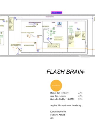
THE MAKING OF FLASHBRAIN: LABVIEW ................................................................3
How the VI Works..........................................................................................................3
CONNECTING LABVIEW TO EXTERNAL CIRCUIT USING LABJACK..................8
SEQUENCE LEDs YELLOW, RED, GREEN AND ORANGE ...................................8
CORRECT/INCORRECT LEDS ...................................................................................9
EXTERNAL CIRCUIT (Daniel Han Log Book) .............................................................10
4. 3
THE MAKING OF FLASHBRAIN: LABVIEW
FlashBrain was made using a LabVIEW and connecting it via a labjack to an external
circuit.
How the VI Works
Structures
FlashBrain VI consists of numerous structures that aid the control and flow of events,
including:
‘PLAY’… Get Ready
(1) Event structure ‘generate array’ linked
to ‘PLAY’ button on front panel. When
pressed by Player, top level flat sequence
structure initiated. Wait timer waits
2000ms before execution to allow Player
composure time. Case structure clears
previous high score when ‘PLAY’ button
pressed – sends 1V to clear node through
labjack.
(2) First frame of top level flat sequence
structure contains for loop that causes the
correct/incorrect LED indicators to
blink for 500ms alerting Player that
sequence is about to start. Case
structure inside for loop has 3 cases:
default=F Boolean,
1=T(true) Boolean,
2=F(false) Boolean
While loop’ Repeats code within its subdiagram until GAME OVER
‘Flat Sequence Structure’ executes each frame sequentially
‘For Loop’ executes sub diagram n times. Iteration terminal, i , shows current
loop iteration (ranges 0 to n-1)
‘Event Structure’ executes subdiagram/ event cases when structure executes
‘Case Structure’ contains subdiagrams/cases that execute when structure
executes. Value wire to selector terminal,?, determines which case to execute
‘SubVIs’ call subVI to top level VI to execute function. Removes repetition in
top level when same structure needed more than once
2
1
Figure 1. SubVI 'FLASHBRAIN
correct_incorrect LED'
3
5. 4
F Boolean commands local variable of correct/incorrect LEDs to remain off, while T
Boolean turns LED on.
(3) As iteration count ranges from 0 to 3 (specified by N) each 3 case is executed causing
LEDs to blink from off to on to off (signal for player to get ready!) via ‘FLASHBRAIN
incorrect_correct LED subVI’. When creating sub VI, must ‘add terminal’ for each control
you wish to use in top level VI
LED sequence played
Second frame of top level flat sequence structure executes random generation and display
of LED sequence. It contains:
(1) For loop executed ‘N’ times determined by user control, ‘difficulty/lights to
remember’ that allows Player input of how many colours in sequence (higher player
input, greater difficulty as more colours in sequence to remember). Shift register feeds
each integer generated into array N times.
Flat sequence structure, contained in for loop, made of three frames that sequentially
execute to generate random number, insert into array, turn on then off LEDs and build
output array.
(2) First frame of FSS contains Random number generator. As only produced numbers 0-
1, multiplied numbers generated from the random number generated by 3.9 and added
0.5 to generate number between 1 and 4. Output numbers 0.5-4.4, integer application
added to round each number to the nearest integer, creating equal probability for all 4
numbers being generated.
1
2
3
Figure 3 Default case. All LEDs
off and 0V supplied to Labjack
Figure 2. Second frame of top level Flat Sequence Structure. Executes LED sequence played.
4
6. 5
Build array function attached to outside of for loop generates blank array.
Insert into Array function builds array with index determined by for loop i
(lights to remember) and elements instered into array each time for loop
executes. Output array indicates on front panel the array generated (not
designed to be viewed by player).
(3) Second frame of FSS inserts each integer generated into case structure
that determines which LED is turned on via T or F boolean control (LED
on when T). Each case also determines voltage supplied to labjack to drive
LEDs on breadboard (0V onn, 1V off), executed through SubVI
‘FLASHBRAIN labjackLED subVI’ (figure4). Cases 1-4 are assigned to
specific colour LED (1=yellow, 2=red, 3=green, 4=orange) and default
case set to F boolean so no LED active when no integers generated (figure
3).
(4) Third frame off FSS switches all LEDs off as F Boolean commands local variable of
correct/incorrect LEDs to remain off, while 0V sent to subVI ‘FLASHBRAIN
labjackLED’ through labjack also turns LEDs off. As all LEDs off, indicates time for
Player input.
Player Input and Call GetKeys SubVI
(1) Third frame of top level FFS contains for loop that calls subVI
‘FLASHBRAIN getkeys subVI’, N times (controlled by player
input‘difficulty/lights to remember’)
1
Figure 4. SubVI 'FLASHBRAIN labjack LED'
controls LEDs on breadboard via voltage input
determined by case structure in top level VI
Figure 5 SubVI 'FLASHBRAIN get keys' reads keyboard input from player and converts to
integer to be compared in array. Also supplies voltage to subVI ‘FLASHBRAIN labjack
LED’ (figure 4) depending on case.
Figure 6. Top level VI. third frame FFS waits
for player input via SubVI 'FLASHBRAIN
getkeys' and inserts player input into array
1
2
3
7. 6
Set SubVI to ‘show front panel when called’ otherwise did not register when keys were
pressed. As integer generated by player input, fed into array controlled by shift register
on for loop to generate output array for comparison in next frame. Wait until next
function specifies 1s wait time between each LED flash.
(2) sub VI made of event structure that executes when arrow keys pressed down
axcording to case structure. Timeout event wired to -1 which instructs event case to
never timeout.
(3) case structure converts arrow keys to integer associated with LED colour
‘up’=1
‘right’=2
‘down’=3
‘left’=4
‘default’= 5 which is discarded (incase any other key on keyboard accidently
pressed by Player)
Again, labjack connection to LEDs controlled by 0 and 1V as specified by case structure
fed into SubVI ‘FLASHBRAIN labjack LED’ (figure 4).
Array comparison + Correct/Incorrect LED + Highscore
(1) Fourth frame of top level FSS executes comparison of generated array and player
array using the equal comparison . Output thread into case structure that lights up
correct or incorrect LED via subVI ‘FLASHBRAIN correct_incorrect’ (figure 1).
(2) Case Structure contains two cases only, TRUE or FALSE. When arrays compared,
results shown in table 1.
1
2
3
5
8. 7
Table 1 results of array comparison and actions caused
(3) Highscore For loop contains case structure that outputs 1
for T and 0 for F cases. When arrays compared are equal, true
case executed outputs constant 1 which is displayed by
highscore indicator, shift register continues to build array until
mistake is made. For next sequence, output is multiplied by the
next T or F value (1 or 0). When T, output 1 executes ‘case 1’
of second case structure (4), supplying 1V to voltage add 1 on
highscore, increasing 7 segment display on circuit (see external
circuit). When F, output 0 from False case multiplies shift
register output by 0, feeding 0 into the second case structure (4),
executing ‘case 0’, 1V supplied to ground state/clear input on
labjack resetting the high score on the 7 segment display.
(5) Final frame of top level FSS ‘resets’ aka turns off all LEDs
on both breadboard and block diagram using two subVIs for the
breadboard LEDs:
FLASHBRAIN correct_incorrect LED
FLASHBRAIN labjack LEDs
And local variables wired to F Booleans to turn off both correct and incorrect LEDs:
FSS ends and while loop continues to execute whole process until Player loses or quits.
Comapare
array, arrays
equal?
Case structure case
executed
Boolean to LED Voltage supplied Action
True True green/correct=T=on g/c = 1V Green/correct LED on
T case fed to highscore for loop (1 point added)
Top while loop executes and new array generated for player to
play again.
red/incorrect=F=off r/I = 0V
False False green/correct=F=off g/c = 1V Incorrect/red LED on
F Boolean for green/correct LED fed to highscore for loop, F
case executes and highscore reset to zero
T Boolean in false case executes stop function of while loop
‘GAME OVER’ message displayed to player, ‘PLAY’ button
resets game and user able to play again.
red/incorrect=T=on r/I = 0V
4
Figure 8. Highscore for loop adds 1 points for each
correct comparison and resets to 0 when incorrect
Figure 8 incorrect
comparison of arrays, F
output generates 0 fed into
case structure, executing 1V
to ground state/clear function,
clearing highscore on 7-seg
display
9. 8
CONNECTING LABVIEW TO EXTERNAL CIRCUIT USING LABJACK
SEQUENCE LEDS YELLOW, RED, GREEN AND ORANGE
In order for the LED’s on the external circuit to light up when the corresponding LED’s
on the LabVIEW interfacing lit up, the information needed to be relayed from the
computer software to the external circuit. This was done using a LabJack UV-H3 data
acquisition board. The LabJack received the information from the VI, and output a
voltage depending on the instructions from LabVIEW interfacing, hence making the
LED’s on the eternal circuit light up.
The LabJack was hooked up to the computer via a USB cable. Before using the LJ, and
OpenLabJack(S) function call is required to initialize communication with LabVIEW
(LJUD OpenS icon). The LabJack must first be registered to the computer. This is
done by hovering the mouse over the LJUB OpenS icon and clicking on “Device
type”, then adding a constant “LJ_dtU3” off the drop down menu. Then hovering over
the LJUD OpenS icon again and selecting “Control type”, and clicking add constant off
the drop down menu and entering “LJ_ctUSB”. Voltages can be generated using LJUD
10. 9
eDAC and LJUD eDO. In this case, LJUD eDO was used because it operates in a
Boolean manner. This was useful because 1 could be interpreted as ON (LED lights up)
and 0 could be interpreted as OFF (LED does not light up). The LJUD OpenS icon was
wired to four LJUD eDO’s (to correspond to four different LED’s) via the “handle
out”/”handle in” arrows when you drag the mouse over the icons. The eDO icons contain
an option “Channel”, which relates to the gates of the LabJack, which are numbered.
Each eDO is assigned a channel corresponding to each of the four flexi gates (FI04, FI05,
FI06 and FI07), which are then connected to separate LED’s. This was done by clicking
on the “channel” option and then selecting “add constant” and entering the appropriate
number. The gates are then wired to the external circuit to their corresponding LED. The
schematics for the LED circuits are as follows.
CORRECT/INCORRECT LEDS
In order for the “Correct” (green) and “Incorrect” (red) LED’s to flash when prompted, a
similar method to that talked about above was implemented. However, instead of using
the flexi gates, the digital output gates “DAC” were used. Two eDAC icons were wired
to the LJUD OpenS icon via the “handle out”/ “handle in” options. The appropriate
channels were chosen to relate to the LabJack gates DAC01 and DAC02 by clicking on
11. 10
the channel option and selecting “add constant”. The voltage was set to 1, which
corresponded to the output by the LabJack (1V). This was done by hovering the mouse
over the eDAC icon until “voltage” was found, selecting it and then selecting “add
constant” from the drop down menu. The reason that the digital output (DAC) gates
were used instead of the flexi gates (FI) was simply because there are only four flexi
gates on the LabJack data acquisition board. The schematic diagrams are as follows:
EXTERNAL CIRCUIT (DANIEL HAN LOG BOOK)
We decided to make a memory game.
I wanted a scoreboard to be implemented into our game that is able to display the score,
which is correct = +1, incorrect = +0. The scoreboard would be 2 digits and hence
requires 2 seven segment displays to be driven.
I did some research online to decide which electronic gadgets I would need.
In order to drive the seven segment display a BCD to seven segment display decoder
would be needed, since I want 2 digits I would need 2 of those.
The circuit should be able to count up and clear the score when necessary (i.e. At the
beginning of the game)
A shift register would be needed, once again, 2 digits requires 2 shift registers.
I bought the following components:
• x2 HD74LS48P Decoder
• x2 HD74LS5192P 4-bit Parallel Shift Register
12. 11
• x2 Common CATHODE 7-segs
• 7414 Schmitt Trigger
• NE555 Timer
• x3 Tactile Switches
I bought a timer chip purely for testing purposes; the Schmitt Trigger might be needed.
I drew a schematic for my circuit.
I wired up my circuit corresponding to my schematic, however something was wrong, the
numbers displayed were very odd. They were not even numbers. I looked this issue up
online, however I couldn’t find anything related. I brought my circuit to Jaycar
Electronics Hornsby to seek for help. A staff member went through my circuit and gave
me some advice. However he was not able to fix the circuit. I decided to try a ‘common
ANODE 7-seg display’ instead.
I connected the replaced the one I had with the common ANODE display and it worked.
Nothing was wrong; all numbers were displayed correctly and correspond to the truth
table nicely.
I thanked the staff member and bought 2 common anode 7-seg displays. I did some
research and found out that my 7448 decoder is for common anode 7-segs only. It can
only be used to drive a common anode 7-seg display.
After reconstructing the circuit I was hit by another problem. Occasionally the numbers
would skip. For instance it would skip from 14 to 16, which it is meant to land on 15.
This time I know the problem was.
I did some research online regarding to switch debouncing. Each IC has a threshold
voltage that it could take. If the supply voltage it too high it might activate multiple times.
I hooked my circuit up to an oscilloscope and observed a giant spike each time my circuit
skips numbers.
13. 12
I am left with 2 ways to solve this problem, physical or software debouncing. Gabi and
Jade are working on Labview and the program is already very complicated. I decided to
do physical debouncing. I studied that hooking the
switch to a combination of 2 resistors of different
values and a capacitor that goes into a Schmitt Trigger
would solve the problem. An appropriate choice of the
2 resistors and the one capacitor would be needed. The
Schmitt Trigger I bought earlier could be used now.
The debouncing circuit looked like this
I studied the formula for switch debouncing, the
formula looks like this:
Vcap=𝑉𝑖𝑛𝑖𝑡𝑖𝑎𝑙×𝑒−𝑡𝑅𝐶
Vcap is the voltage across the capacitor
Vinitial is the initial voltage (supply voltage)
t is time in seconds
R is the sum of the 2 resistors chosen
C is the value of the capacitor
I would like Vcap to be smaller than the 74192 Shift Register’s threshold.
After calculations I chose 330Ω resistor, 5600Ω resistor and a 1µF capacitor. I also added
two 1MΩ resistors to pin 3 of my two 7-seg displays. This fixed the bouncing problems.
14. 13
I finalised my schematic by adding in the modifications I made:
However there is one more problem, the supply voltage bounces when I switch the power
on. This can be fixed easily by letting our Labview program activate the ‘Clear’ switch
when starting it (see ‘how the VI works’ on page 3)
I informed the problem to Gabi and Jade. Then I started to work on the LEDs we are
going to use for our memory game.