1. LAB 4 Report Bruno Diaz
This Program creates an acceleration profile, what type of profile will depend on a user input,
Via 2 onboard buttons. The LED lights on the development board will indicate when the button and
profile will be generated and when the program finished successfully.
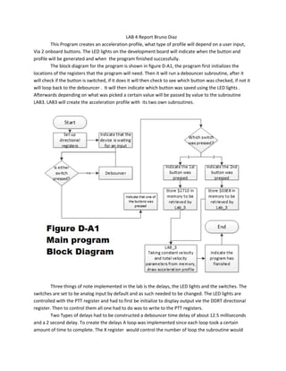
The block diagram for the program is shown in figure D-A1, the program first initializes the
locations of the registers that the program will need. Then it will run a debouncer subroutine, after it
will check if the button is switched, if it does it will then check to see which button was checked, if not it
will loop back to the debouncer . It will then indicate which button was saved using the LED lights .
Afterwards depending on what was picked a certain value will be passed by value to the subroutine
LAB3. LAB3 will create the acceleration profile with its two own subroutines.
Three things of note implemented in the lab is the delays, the LED lights and the switches. The
switches are set to be analog input by default and as such needed to be changed. The LED lights are
controlled with the PTT register and had to first be initialize to display output vie the DDRT directional
register. Then to control them all one had to do was to write to the PTT registers.
Two Types of delays had to be constructed a debouncer time delay of about 12.5 milliseconds
and a 2 second delay. To create the delays A loop was implemented since each loop took a certain
amount of time to complete. The X register would control the number of loop the subroutine would
2. produce but calculate the number of loops needed the number of cycles per loop and time per cyle also
needed to be know. The S12 runs at 8 megahertz so each cycle meaning each cycle takes 125 nano
seconds to complete so that we need (12.5E-3/125E-9)=100,000 cycles to load the loop we will first have
to load the x register with how many times we have to loop which is X. then we have 3X cycles for every
time the program loops (since BNE takes 3 cycles to loop)and the decrement X is X cycles plus the one
time the one time that the program gets out of the loop which is 1 cycle. Ultimately the number of
cycles burned through by the value in the X register is 4X. So the value needed for a 12.5 millisecond
delay is 100,000/X=100,000/4=25,000=$61A8 base 16
The 2 second delay was not as straight forward. A decrementing counter like the one used in
the debouncer could not be used here as the number of cycles needed to create a 2 second delay far
exceeded what X register could hold. A solution to this was to create a “two dimensional” decrementing
counter. One could run an entire decrementing protocol with X and then have the Y register decrement
every time it finish and reload X to do it all over again until the Y register read 0. One major drawback to
the 2 dimensional counters was the math was very complicated,. Finding the equation itself was pretty
straight forward , all one had to do is use the same equation for the 1D timer and make it dependent on
Y and get number of cycles =4XY+4Y (this was my revised calculation, my initial calculation was off as I
will discuss later)but working backward algebraically to a desired target number of cycles was very hard
and on top of that the counter was not very precise. To rectify the problem a hybrid system was
implemented. Combining the wide range of the 2 dimensional counters and the precision of the 1st
3. dimensional counter, one could get the number of cycles within the range of the 1 dimensional counter
by using the 2D one, this would get you within 0-4 cycles of a target number of cycle. An additional level
of precision could be added by repeating INX 0-4 times to get to the absolute exact number of cycles
needed. The method to see what values for X and Y were needed was simply to use a spreadsheet
(Figure T-A1) with the formulas inputted to get it near the desired range through trial and error.
After designing the entire project the next step was to simulate is in full chip simulation by
manually inputting the user input in memory via code warrior. This was done to test whether the
program fundamentally worked regardless if the right kind of implementation was made on the
hardware side for the switches and lights.
The first thing to fail testing was the 2 second delay . Despite the spreadsheet saying using these
values would cause the microprocessor to go through 16,000,000, the number was off as seen in figure
T-A1 . After crunching numbers it turned out there’s was an error in developing the equation for the 2
dimensional counters. The right equation was inputted into the subroutine and as we can see in figure T-
A2 The desired numbers of cycles were run by the microprocessor.
After those test were the program running on the actual chip was testing. There were some
complications. It turns out some assumptions the way that outputs and inputs were worked was counter
initiative. A 0 in the AD registers meant that the user pressed the button rather than a 1 and 0 in the
PTT port is what turned the LED light on not a 1. So rather than rework the math I simply one
complimented the receiving input from the AD port to allow the program to run regularly, the same was
done with the output values meant for the LEDs. After that it turned out one of the jumpers for LED 3
was taken out , so one from switch 4 (which was not being used) was taken and put in its place.
One final hurdle had to be overtaken. For some reason despite the LED light indicating that the
program had run after I pressed one of the buttons, no acceleration profile was written. After running
through the program step by step (made possible by setting all the counters in delays to 0001) it was
found that the program could not access the memory, the desired memory locations were permanently
stuck in $FF and no value could be stored , from storing an accumulator or from a stack. As the program
was tested in full chip simulation with no problems it was assumed that this may be a hardware
problem. It was however found that the memory from $2000 to $3000, so rather than mess with the
4. hardware , the profile, parameter passes and stack pointer were moved to that range and the program
performed perfectly . The results of the final tests are shown below.
5. After running the final test it is shown that the values match what was expected in lab three according
to which button was pushed. In conclusion after debugging the program it was a success.
6. After running the final test it is shown that the values match what was expected in lab three according
to which button was pushed. In conclusion after debugging the program it was a success.