SlideShare a Scribd company logo
1 of 38
Download to read offline
THAIMALTA MOATAHONTIRANIMAMITTEUS009762251B2
(12)United States Patent
Josefsberg etal.
(10) Patent No.: US 9,762,251 B2
(45) Date of Patent: Sep. 12, 2017
(54) ULTRA LOW PHASE NOISE FREQUENCY
SYNTHESIZER
FOREIGN PATENT DOCUMENTS
woWO 03026133 A1 3/2003
(71) Applicants:Yekutiel Josefsberg, Netanya (IL ); Tal
I. Lavian, Sunnyvale, CA (US) OTHER PUBLICATIONS
@(72) Inventors: Yekutiel Josefsberg, Netanya (IL ); Tal
I. Lavian, Sunnyvale, CA (US)
@(* ) Notice:
Gismero, J. etal.,“9 GHzphase locked oscillatorusing a sampling
phasedetector.Application to VSATlocaloscillators(18-27GHz),”
European Microwave Conference, 23rd IEEE, Oct. 1, 1993, pp.
784-786 .
(Continued )
Subject to any disclaimer,the term ofthis
patent is extended or adjusted under 35
U .S.C . 154(b) by 0 days.
(21) Appl.No.: 15/379,860
(22) Filed: Dec. 15,2016
Primary Examiner — Dinh T Le
(74) Attorney, Agent,or Firm - Remarck Law Group
PLC
(65) Prior Publication Data
US 2017/0099058 A1 Apr. 6, 2017
Related U.S. Application Data
(63) Continuation of application No. 15/229,915, filed on
Aug. 5, 2016.
(Continued )
(57) ABSTRACT
(51) Int. CI.
HOZL 77087 (2006.01)
HO3L 77085 (2006.01)
(Continued)
(52) U .S. CI.
??? ............. HO3L 7/085 (2013.01); HO3L 7/07
(2013.01);HO3L 7/099 (2013.01);HO3L 7/24
(2013.01)
(58) Field ofClassification Search
CPC . HO3L 7/085;HO3L 7/07;HO3L 7/099; HO3L
7 /24
(Continued)
A system for providing ultra low phase noise frequency
synthesizers using Fractional-N PLL (Phase Lock Loop),
SamplingReference PLL and DDS (Direct DigitalSynthe
sizer).Modern day advanced communication systemscom
prise frequency synthesizers thatprovidea frequency output
signal to other parts ofthe transmitter and receiver so as to
enable the system to operate at the set frequency band. The
performance of the frequency synthesizer determines the
performance of the communication link. Current days
advanced communication systems comprises single loop
Frequency synthesizers which are not completely able to
provide lowerphase deviationsforerrors (For 256 QAM the
practical phase deviation for no errors is 0.4 -0.5°) which
would enable users to receive high data rate. This proposed
system overcomes deficiencies of currentgeneration state of
the art communication systems by providing much lower
level of phase deviation error which would result in much
highermodulation schemes and high data rate.
(56) References Cited
U .S.PATENTDOCUMENTS
6 ,085,151 A
6,122,326 A
7/2000 Farmer et al.
9/2000 Jackson et al.
(Continued ) 17 Claims, 22 Drawing Sheets
1900
1904- - - -- -
1910 1914
1906-
Fractional-N
Synthesizer
Digital
phase
Detector
EN
Vin ?? outina:
???? Primary
VCO
Main PLL-
o comew TI N .1916SW
control 19081
Sampling V12 Referencephase VCOdetector
* 1920
1922 Sampling ?
1918
!
US 9,762,251 B2Page 2
Related U .S.Application Data 8,378,751 B2*
8,704,562 B2*(60) Provisional application No.62/181,221,filed on Jun.
18, 2015. 8,816,777 B2*
2/2013 Fagg ................ HO3L 7/185
331/10
4/2014 Nicholls ................. HO3L 7/185
327/144
8/2014 Szilagyi ................... HO3L 7/08
327/156
10/2016 Kishigami et al.
6 /2017 Cao et al.
9,470,784 B2
9 ,689,983 B2
OTHER PUBLICATIONS
(51) Int. Cl.
HOZL 7/099 (2006.01)
HO3L 7/07 (2006.01)
HOZL 7/24 (2006.01)
(58) Field of Classification Search
USPC .... 327/147–159, 105–107, 111-114; 331/2,
331/11, 18, 40, 47, 1 R , 10
See application file for complete search history.
(56 ) References Cited
U .S. PATENT DOCUMENTS
Liman, R . et al, “Noise in Sampling Phase Detectors for RF PLL,"
Proceedings of the 39th European Microwave Conference, Sep .
29-Oct. 1, 2009, Rome, Italy, pp. 480-483.
Partial PCT International Search dated Jan. 9, 2017 for PCT
International Application No. PCT/IB2016 /054790, 3 pages.
Teng, K .H . et al.,“Microwave Phase-Locked Loop Circuit Devel
opmentand Efficiency Improvement,” IEEE,High Frequency Post
graduate Student Colloquium , Sep. 8 and 9, 2003, pp. 128-131.
U .S. Appl. No. 15/229,915, filed Aug. 5, 2016 , Josefsberg etal.
U .S . Appl. No. 15/379,915, filed Dec. 15, 2016 , Josefsberg et al.
Henrickson, L . et al., “ Low -Power Fully Integrated 10-Gb/s
SONET/SDH Transceiver in 0.13 um CMOS,” IEEE Journal of
Solid-State Circuits, vol. 38, No. 10, Oct. 2003, pp. 1595-1601.
PCT International Search Report and Written Opinion dated May
23, 2017 for PCT International Application No. PCT/IB2016 /
054790, 18 pages.
6,366,620 B1
6 ,657,464 B1
7,102,446 B1
7,391,839 B2 *
4/2002 Jackson et al.
12/2003 Balardeta et al.
9/2006 Lee et al.
6/2008 Thompson ................ HO3L 7/16
327/156
HO3L 7 /10
331/16
7,545,224 B2* 6/2009 ChowVIZUVY CHOW . . .. .. . .. .. . .. . ..
7,656,236 B2
7,737,880 B2
8,049,656 B2
2/2010 Williams
6 /2010 Vacanti
11/2011 Shani et al. * cited by examiner
US. Patent _ Se[0.12,2017 _Sheet1of 22 US 9,762,251B2
-f00
{; 4
R + *
+
' ;6
m
FIG. 1
200
202 23# 206 238
FclockReference
Clock
oop?? FoutPhase
detector VCOfilter
Fclock
Fout/N
fuji 'ituff
_ ' _
?? ?SW control
FG, 2
U .S . Patent Sep. 12,2017 Sheet 2 of22 US 9,762,251 B2
300
304
304
Fclock
Fout N
FIG . 3
8+
26.7 nF
winninnnnnnnnnnnnnnnnnnR2
989
402 129nF
FIG .4
U .S. Patent Sep. 12, 2017 Sheet 3 of22 US 9,762,251 B2
500
502502 504
a po 2
INPUT OUTPUT INPUT OUTPUT
wwwwwwwwwwwwwwwwwwwwwwwwwwwww
entretenimSAMPLE
CONTROL e
o
SAMPLE
CONTROL ?
FIG . 5
604
RE
INPUT
mnomnomnomnomnomnomnom ERROR
VOLTAGE100 MHZ
INPUT SRD
606
r
FIG . 6
002
o
M
Thanoffarmen
ThanemWh
menerima
FIG.7
gorenewemamanewmy
tamamen
?? ??? ???????. ?
Thom
óóóóó
US 9,762,251 B2Sheet 4 of 22Sep. 12, 2017U .S . Patent
U .S . Patent Sep. 12, 2017 Sheet 5 of22 US 9,762,251 B2
800
- DECISION
SOUNDARY
ofO OLOMBO
oogo fotosooooofoto 's
30 gout 50 tot
Ooo Soo ooo
Ooo Sato ooo
ooooooo
o outdoomemoryand I
too too
0
0
FIG . 8
U .S. Patent Sep.12,2017 Sheet6 of22 US 9,762,251 B2
900
Phase
Qe
X
I
FIG . 9
1000
Free-Running VCO
Phase Noise
PhaseNoise 1002
V -1004-1004
Shaped VCO
Phase Noise
you
Loop
Bandwidth
FIG . 10
U .S. Patent Sep.12,2017 Sheet7 of22 US 9,762,251 B2
PLL Noise Model -1100
- 1102
www.reference oscillator
1104
an VCO
-phase comparator
frequency divider
AbuanbaloaSIONaseud
ZH/gpJazsayjuks meglio
comonomom
momentyou
wow.o
1108
Mama m 1106e
nesasi
VCO,resistorofLPF
afterPLL response
Loop Bandwidth
OffsetFrequency(Hz)
w phase comparator
frequency divider
afterPLL response
Measured Phase Noise
40 mmwegg e gnupugang minginn
1 } { 11 } } {{} } { } 111111 1111
1: { } } } : 11333 in 1 11 1 11333
L w en induit tebreiten hatdie hul an LLLL
} { 1 } 113 1 1110
$ 11 }}} L 11 fin ! 11111
i II } } }
1711
1933 SI NUN . 113
lilil 11111333
ten goingo the song 2074
} { } 110 111 11B
{ { { 1 } : 1188 m 111111
imenufimmmmmmhmmmhmmmmm. mmmmmmmmmmml limmmmmelnmmhmmdirmiehen min i málne
{ 1 } } } } Pri 1101
Illim{ } ! ! !!!!!
{ } } } {}} Lipi
- ill 1113331
11111333 ? 7777777 - 7777
} 11113331 } { { 1 }} } UN 10
----------
13384 ??? ???? ?? ????
{
} } }} 811 U11 ---
SingleSidedBandSpectral
Density(dBc/Hz)
wwwwww -
3311
------------
etto{
00 1111111
iniwmilletinimeni
1}331111
intentanham binimin Webminmin
{ { 1 } }i n t IT
i } ! !! ! ! ! !! ! ! !
for theHHH -- the mind the will feature HH
{ { { 11 }}} 1 } } Vind 1111
} { i}}} : 11333 111 111 1 111
1 } { { {1 }} L } , } f
1 . 333 } }} : 1133 110 1 1111
$ 111 : 1113 In
i { { { nu ! ! ! 1
** ]* 733 ***1701133 * 11111111 ***171 MI " 1711x31
1110 1111111111
1 . 311111 11113331 in } } { : 111333
140mfumantridebitishie mandarinimahasiswidant
Uit wew
thestoodstotkototowant
10 106102 103 104 105
OffsetFrequency (Hz)
FIG . 11
U .S . Patent Sep. 12,2017 Sheet 8 of22 US 9,762,251 B2
1200 mm Carrier
- In-band phase noise
1202 --Noise peaking due to
loop transfer
function
VCO inherent
phase noise
?
A Spurs
20 log(Na) 20 log(N4) Synthesizerphase
???fqYNy>N2
FIG . 12
1300
-Ps
Single
sideband
phase
dB noise
Pssb
1HZ BW
Af my home
Single sideband phase noise
FIG . 13
U.S. Patent Sep.12,2017 Sheet 9 of 22 US 9,762,251 B2
{ 43
1406 03 ( 4 )
|ns Output
- 2 2
XQ Phase
detector = {G 2
{{F{ q fz}-{x} }} - 1402
4 Aa
1 ???
-34 :
N (F £9(2}--fr}{
Phase
ct 3
| Vcd2
O ---{ 434
?, , , , , , , , , , , , , , ,= = = = = = = = = = = = = = = = = = = = = = = = = = = % % % % % % % % % % % % % % % %, , , , ,
4 ???
{ { 6
FIG. 14
5 }
??? 2 1508???{ 59 15061506
- 2
CoubS32313 ,
generator Se .
detector
Try 3Q
????????????????? VCOfilter
*
* {
FG. 15
U .S . Patent Sep. 12,2017 Sheet 10 of 22 US 9,762,251 B2
1600
1606 8091
SOURCE
ATRA
IMPULSE
TRAIN
GENERATOR
1602
u
to learn
EV N7604
toway
FIG . 16
1700
w
RelativeOutputPower(dB)
manniframanmarafinamfuatananinawwwwwwwwwwwwwwwwwwwwwwwwwwwwwwwwwwwwwwwwwwwwwwwww wwwwwwwwwwwwwwwwwwwwwwwwwwww wwwwwwwwwwwwwwwwwwwwwwwwwwwwwwwwww wwwwwwwwwwwwwwwwwwwwwwwwwww wwwwwww wwwwwwwwww MANAMA
innen winnennennen
12 4 6 8 10 12 14 16 18 20 22 24 26 28 30 33 34 36 38 40
Frequency (GHz)
FIG . 17
U .S. Patent Sep. 12, 2017 Sheet 11 of 22 US 9,762,251 B2
1800
1802 1804 1806 1808
SW
control
Prinsen Fout FoutfinalDDS 7 FrequencyDigitalphase
Frequency
Detector
Fp2
Primary
VCO18
DDS clock 1810
Main PLL 18164 + 2
1814 1812 TFT
for1820
rexoL2 phases????
VCO
For Sampling V12 Referencephase
VCOdetector
SamplingPLL !1822
|18181818
1824 1822 L1824
FIG . 1819001900
1904w w
1902-
1910
1906100
Fractional-N
Synthesizer 1914
wiewirim
roxo Fo?cxo Digital VAVanDigital
phase
Detector
FoutPrimary Fout outfinalPrimary
VCO
wwwwwwwwwwwwwwwFUN 7912
Main PLLN
SW
control
CCCCCCCCCCCCCOLE
www 1908. * * * * * * * * *
Sampling Referencephase
detector
† 1920Sampling PLL1922
1918
FIG . 19
U .S . Patent
2016
2002
ras
2004
SamplingPLL
comb
Comb
SamplingVusDCswitchvel
Loop
phase
generator
detector
filter
TCXO
VCO
Sep. 12, 2017
2008
2006
Vid
2010
2012
No
DigitalPLL
mm
DigitalPhaseFrequencyDetector
2018
Sheet 12 of 22
2014 FIG.20
US 9,762,251 B2
2102
2100 PHASENOISE(dBc/Hz]
Ôägggaje?
??????????
Hummer
100
AP1396MB
minin FIG.21nnnnnnnnnnnnnnnnnnnnnnnnnnnnnnnnnnnnnnnnnnnnnnnnn
1427MHz1
1K10k
FREQUENCYOFFSET(Hz)100k1M
NISSSSSSSSSSSSSSSSSSSSSSSSSSSSSSSSSSSSSSS
nininnnnnnnnnnnnnnnnnnnnnnnnnnnnnnnnnnnnnnnnnnnnnn
1696MHZ Yooo
wysymy
w
10Minninnnnnnnnnnnnn
meno
H
--2104nnnnnnnnnnnnnnnnnnnnnnnnnnnnnnnnnnnnnnnnnnnnnnnnnnnnnnnnnnnnnnnnnnnnnnnnnnn
mene
100M
21122110-21082106
IST?79L*6SN77JOETJ??4SLIOT‘ZT`d?sbu?d'Sin
FIG.22
US 9,762,251B2
#23?
Frequency[Hz]
303
Z'
????
.
2-30
00
Z-
7-8
ff}}
ZHf}{0;L
?
?
?f
*};
ffiii;ii
i.
{
}
}{
}}
}
}
}
--06f
}}}}}
?
?
'3!:-:-
?
???|?
?
??'??
.??
?
?
?
?
?f ???
?
;_
?
;_
??????
;
???:;
?{{
{{
{
{
{{{{{{{{{
2214??
$ % $ #
Sheet 14 of 22
-222
'??'?
?????????
???:;;:,?????????????????????????????????????????:;:;
??????????????????????????????????????????????????;:
??????????
????????
}}}|.??{;
?????:'.?i
?????????
??????????
'!!?:}}}
???????1
www!!??????????????1
:%:???
??????????????????????????
?????????????????????
??
????????????????????????????????????????????????????????????????
???????????if
??????????????????????????????
?????????????????1??????????|?????????????????????????
???????:;!???????????????????|.||?????????????????????
????????????:;;;:1????????????????????????'?"'
?????!!?!
????????'?!?????'?
???????????????i
:
i?
??|??'?-i----!???-)-----+--|??-'+?????????4-----++H-!-+-??????????????????:?????.-:4-------+-?-*-????+|??????-
-
A++H
+
-
-
?????????:!?????????????????????????????????'_
????????????????????|
????????
???????????
???????}}}
???????+?????;r
-
ff??????[--???????????????????????????;?????????;:???????
???:;;;.;i????????|.?;??|??
;;;;;;;?
---
X
:
?
;
-
f
-
-
F
--?????
?:fr
????????i?????????
?????????
??????????????????
?????????
'!!?:;;;i
?????????
????????
.!.!-:::?:
?;?!?:!.-
.?.!!??:}
????????
!;fi.
??????????????????:
;
ffy
i
:
?????????+ffffe
?
???????!?'!!!'''1
??????????????????????????:;-;????:;_;?????:???????????????????
?????????????????????????
?????????
?????????????????
?.?..........?...
:
-.
..
i
M.....?.??.:???i..??.......????..????.?.(.;.l????????????
???
??..L.-???????.????.........????.???}
?????????????????????
????????
?
??????
????????f
?????????????????'?????????;!;;;;????????????:;''.????????
?????????
?????????!}}}}}}}??????????????:3
??????}}}
?????
-yr-
fff---;;r;":":-'
:;ff'ff
*f;*-
g
***
f
-;
;-i
$;;f:"
limam???
2210
??2202
?
PhaseNoise(dBc/Hz)
??
??
- ?? ?.?
?
??????
???????
??
????????&{???
?
{
{
{
{{{{
?
_;_;_.;
??
?????????
-- --
2238??
.
?
?|
?
2206
*
'
;
?????:
?
}
?????:}?-.;..-..-..???????.-:.-.-........
_ Ser0.12,2017
?;
1.??????
??
?
?
??????
?
?
?
?
?
?????
?
?
?
?
??????
.-.........
.
L
:}?.?.?.4.?...-.?....--!tit;.}.?.?..........??????.?..?-...f-.-.-.???????.
?
?
?
???????
?
?
?
??????
?????
fgta
}
OF
??FutaP.????
?
???
???
??????????????
????
??
?????????????????????
???
???
?????????????????????
???
???
??????????????????????
?
??
??
??
???????????'
??
??
?????:;???????
A;;
---
-
----
?
?
;_
???:;;_;_;_
?
??????
.....????;:!
?
|.
?
?
??????
?
?
?
?
?????
.??:;_;___.__-.;.....???????..
?
?
??????
?
?
?
?????
?
?
?????
????????
??? _
i|
!????i
?
?
..??
!..|......!???:???
i'
??????i
i
};.;:?i
Filter
?
- --
??
??
?
{
{{{{{{{
-
?????????
??????????:;!???!f
??????:;?????????
????????
?????:;'?????????
??????:i????????;?????????
?????????
?????????
??-'_i_::?????
:--?-.????||?:1--------'-!;:????????:'!'.???.?????'_}£
?????????????????????????????????????????????????????????????????????????????????????????????????????????????????????????????????????????????????????????????????????????????????????????????????????????-
.?
?XTAL
OM-
AllNoiseContributors
US. Patent
?00}22
U .S . Patent
2300
AllNoiseContributors
otowoween
wwwb
ili!!1
iL
--
ili:
1
I!
?
. . !
- I -
-
- - -
-
-
N
VCO???.
PDFilterDivmom.TotalPLL
.
U?!!
III
-
}
liit
liiii!}
Sep. 12, 2017
Limmmmmmmmmmmmmmmmmmmmmmmmmmmmmmmmmmmmmly
-
+
+
ew
- -
----
--
!
!!
I
--
.... i
.
1
Milit
-
-
-
--
--
PhaseNoise(dBc/Hz]
TotalOIP
papapatay
}primit
11111illiL11
1
ii
lin
Tiit
liiiiii
i111111*
::}liitI
lip1Tf1!!11ii!iiti
1::11il
ittiili111!!!ii!Ilir
--S
.Lil.-.-L-IIILJU----I--LLLL!!11---------
--
!
lif}I
till111!!!!iiili
!!ii!
i
?lili
:11
---
tit------†
H-------
----------
iii}
1:}}}L{i}iirti
!!!!
i
i
!!ili1iliill
!!!!
iiIPIN1111ListItiliit
****1717*****
7:7
!iii!!!!
!!111IIliini
iii!!!!I
iit!i!!!!}
--ISLITI---L-LIIL
L
---
TUL-LILIII11C-LNIH
1:Ah!i1Interventioningangpapuntang1!111!iliistinei
:}
alarmantneilli
II}!!
1}1illi*}}{:11
I:}liitwalilill!Iiilis:
·**of***-lampa-**
**-*fosfor11111***-**17******
*itlayat11togofor""!**forInterior
irayonutIlilin
gawegestioniiPrima
interesniLaweyan!!!!!
bi:111
iii!!
I111!!
!Ilini
nisl
1
!!
:?liii}!
}lill]111!!
iNiliit
kaupyti
II!!
-
?ji-iiiiiii?---7-
--7-7MT--?Wit---?ir
I!!!il{}
}tilII!!!i
Fit
III
!!!
!!iiif}I11
1{11.!!!!
1111
VIII.
{!!!!!
-I.LL1.li.--LIIILIJU..
-LLII-andu_l_
lenrakkauttamann
Biii!
Lii!{}1111
liit!
!
Lii!!!!i11listI
till!
!!!!
INI!
liit
--------11----------ft!}--------
**------*111!--------ge-1
***
wwwwwwwwww
www.
a...à....
iniiniind
n.2306
-1204
2302
- -
-1304
-2308
-
--2310-2310
-
-1404-1504 -160
100HZ
Sheet 15 of 22
-
etScale).ExportPlaipa
m23122312
1KHZ
10MHZ100MHZ
10KHZ100kroz1MHz
Frequency(Hz)
2304
FIG.23
US 9,762,251 B2
FIG.24
US 9,762,251B2
2404
Frequency[Hz]
Hzfk
'
Hz
_
10kflz
_
300kha
{
{
'
Hz10
'
M
'
Hz100MHz?100
?70-
????????????????????????????????????????????????????????????????????????????????????????????????????????????????????????????????????????????????
?
?
?
?
????
?
?.-
:1i''
;
-&
242???
-- -L .. .. ..?
_Sheet16 of 22
Q-????2??
:
'
'
;
??:;;
24;2--
2408
?
PhaseNoise(dBc/Hz)
??????????
?????????
?????????
???????
?????????
?????????
?????????
!????????
?:;!|||||??;_
;!?:?
??????????????????
?
?????|
??????????????????_?????????;
??????
{
ff-
?
'
?
-
-
-
-
-
-
-
'
:
'
fff
-
-
-
-
-
-
ff;
-
-
:
-
-
f
-
-
-
-
-
;
;
-
:
:
;
;
-
-
-
-
-
-
-
{
g
38
5
3
:QX
-
'}{??????????:33
ff:;
??????????????????
??????????????;:3
?????????????
???????:i??????????????????
????????
???:;i'}
????????
????????????????????????????
????????????????????
????????
??:;
-
-
H
T
-
-
-
;
:
;
-
i
:
;
1
-?--?--:--;:?:rrr
-
-
-
.
--
-
-
r
;.----;--;-;-?????;:---F--:-'-??????----?????
????????????????????????????
??????????
;;M;.::|??
????????
??????:;
_f_?.?????????????
??.?;:;
????????!.?|???????
??????????????????????????;%???_
}
i_
;
ww!
;
_
'
_
;
??
:::-----?-?'?ri
?*:---?????':"-;";fif??????????????:;""'"'";-*F
-'
rT?:*-*???????"?'--;*---;"f
"
r';;;
????????i?:????????
???????????
???????????
?????:i
?????????
????
?????
|.??????
?????
?????????
???????????
??????:???;_;_;_;Ii??
?????
?|.-.-------i
H
.
-
.
-
.
-
;
-?
F
-
'
-.'.--?--?--|?;-F-;.--???????----------????-.-.-.-*..-.--?--j
-
-
f
-
i**--------..*-***
???????????????????????????????????????""????????????????????????
?????????
?????????????????????????????
????
??????
??????????????????????????:;???????????1?????||?
;i.--.???.??.14?????-i-;*-,--?????.-.|.????i.-???????-------??-.-.-,?-'?.;.;;----------j--?????,?????-.-..-..|??.???.--+--++1-4---------"*+-?.||?
???????????????????????:;;;;??????????????;!|?
??????
?????????;_;_;_;?!;!?????????
?????!';
???????
??????????:_'{_}|?:??????????;;;!!(!??
????????
??????-???????????????????????????????????????????????????????????????|???+??-f??????????????????????|4?
?????????
????|??
??????:;?
??????????
?????????
????????
???????:i?????????
?????????
????????
??:;'f
'
ij
_
f
l_??????
???????:i
????????'_???????:;
?????????
.????.???!??-?-J??1-!--!&i?????-!?-???????????.??????????1-?'-i
-
i??????????????3;
??????????????????
????????????????
???????|??????????_;;;;'}|
f_'??????
????????
???????|??????:;.f??|.|??;;
????????????????'?????????
......;!,:.i.;!...?!.?!,'!,'...
...........!|;!!........??;:;.'i...
?????????
?????????
?????????.!f'.????????????;!|?????????
?????????
?????????????????????????????????!';????????
?????????
?????????
??????????????;!|;????????
?????????????????????????????????????????????????????????
??????????????????????????
?
1..-..;
|
|
–?!
22436
. ?
.-.-.|.
????:;_;'_
;'iifi_
.-00£-
?.?.?.??????
{2}O}-----
c}
Sep.12,2017
?
?
?
?
????
?_
?
?
,????
? . ?..?. . . .? ??
--..
d
{
€
{
Ob??
.--Mit?
......
!
|:!!|
.......'
Filter
?????????????
?
?
SjoinquiuoaSIONIV
?
X
'
AL
?
_2400
U.S. Patent
US 9,762,25182
092?
(ZH)Aguonbely
ZHA{_
?0
ZFHWN£
ZHf0f;
£
_
ZHA
ZHfVAN001
_
LHWNQ;
{
{
{
|!'{{{
?
...09£
-0gt
??
;
;
;:;;;_;
????
3+...+
11
111
11
1
*
---------
:::
??
.
.;;
??
?????????????????????????????????????????
???????????????????????????????.
?????.3.??.i.1????????????????????||???|???.?.?:???????????:L?????????????????????£???.???4
,
11.}?..?????.??????????;
?????????????????????????????????;:i_
;.}}}}
;;_;'.?.'??.????????????????????????!?
?????????????????????????
???????
????????????.????
????|?|i|.?????????
}
}?????
???????}_
???:;ff
???????
?.?.?|';??????????????:;;.;}}}.?????
?.?.??????
???????????????????????????????????
????????
??????.?.?.'.i
,
l|;.?.?.??.;,??....??£;&.???.???..?.??.??.;:££i£-..;.-..;?????|..|???..?.?.?;114
i??.?;-..??1...???????.:-
???????????????????
?????????
????????????????????????:;°
???:;;__
????????
;_;_;;!|;;???????????????????
???:??:'?
??????
????????????1.IJ??.????????????????1?????????????????????????????????????-?'???????????????????????????????????????????????????????????
!.?????????????????
}}????????????????
???????????????????????:;]
;;,'?'
?????????
}}}}}}'}}.!???????|
:
?.?4
4????
???????'?
.
?????
??
;.58
Sheet17 of 22
??
?
??
??
??
????
80-C
{
{
{
{{1!{{
?
{
{
|{{{{{
??A.
?
---
ºi
---L}}i;------II/{_L
---::__*_----
?
-1-----}_{{--
1-*-----{{}}{{
i-
-CQS
? ??
PhaseNoisefdcfdz
?9f392
?
??'????
?????????????
?
};**ff|||.
??????
;ffff.!!|.
?..??.|.3...,i
.
I?.
???
|?|????f
1?????????
??????????
?????????????'???????????:;'
?????????
1.?}}}}}}?????:!???????????'_;_;}
.????????????--????.1...........?.'...???.?.?--..??????…?.;;
?
??-
;
;
;
;;??
!
*
***
*
*
*
*
*
-
?
?
????
882???
???
?
?????????
?
?
?
??
??????
??
??
???:;
??????
-
+x-4
2
11
11
-11--244
--------
1x1:
--{x
C{
---
--
?
-
?????????????????????????????
AC-.....-.
falf;-g
--
{J
???
_ Ser0.12,2017
-;-
??
?????????????????????????????????????
????????????????????????
?????.?{{|???????????????????????????????
??? ??????{il????????L.????????.?????-1??.?????????????????.??.???L
'
f??????
??????1;_???????????????????
??
__}}}??'
||||||i??????????1??????????????:;'
????'???????????1??????…???
.?£?1|1???.-.!.-.-3
1?;L;---}..?.???.??Li-.--.?..??-f&;?J..?
????????????????????????????????????
}}}}}}}}????????????????||????????'_
????????????????????????????????????????????????????????????
?????????????????????????
?
?FWLX
????
-.-
??
';;;;;;_;_;
?
"f
f?
QQ';'
???
-
?
*
???44??????????????????
??????????
SjoinquuoaSIONIV
009/
US. Patent
905
US 9,762,25182
$-39
(zh)Aouonbang
?Z
}}
?2
??0}{g}}}
}}}}}}}
}{0
?2
;;;
????
-09£---08£-
- --- --
{{{Hi
???
?????????r?:????????????????????r?????????????????;
????????r
;
-
r??????????????????
-.??.-.;.?.-1..??.?1.........??.??..J.:*-.-..-..-.....,1-1-?.L
.
:
ii........'-.-....?.?.-1:.-..-?..£.:.£££
*
.|...?J.;]--).;;
??????????????????
?|????f
:
i
???????|:??????????
???????
;_}|??????????????????????!?????:}|
?????????????}}}?????????????:;:;
???????
????????-????.'1???????????????????????????????????????????'£???????????????????
?????????
?????????????????????:;?!???????|??'__?????
»«??????
????????????????????????????????_'.}???????
||??????
?????????????:;?;?????:!'!
'P!;;.????
?-HOCHYWO0X;:'
- g-' ?? -
?-£-dgt?
_f
_i
MJif|
-------LiL
-
***---
-----
-
----
--
i4-------------
*
?????????
}
--
4------
-
-: :-
???}}}:!?????????????????:
f
????"f
fff|???????
.}|???????????????????????????????????1:
|???????
???????????????????????????????????i???
_
f
i??:???|
;..1..I.??????;???.£????...'.,-1.3.3,?:.J........??..?A.|...?..?.:..
i
A
(
,
;............???
;_;'';;;'?????????????????????????
??????????
;_;'???????????????????????:;_!??4?????????????
}}????1.;;???||||||????????????????????
?????}}}????????
?90£[???@809
Sheet18 of 22
-- - - ??…
. .
-
00Z
--<---
3:!------Fi{}{C
!
!
!
t
...
Crea.
+
---
LiL---
i!i;;;;
ai------{{it--:-1--
L
!
:
+
i
;
Phrase'Maise[d8cffe
}gc
?. --- -
----
?. ?
--
fed{€}{OL
-
;?
?
--- ---
-
--
{
{
????????|.?
_'.???????????????
||?;;;?!;.)-f?????????:!!i_
|if
|:1?
?????????????????????????????????
}}}}}};1???????????????????????????
?????.??..??????.???????.?????????????.?.????..??-.??????:???????.???.??.?.?.|?????.???.??.:-.-.-.-}}}
?????????;_
:?f
:
i
???????!;
f_{_{|???????????????????i:????????]:
?????-
f_;_???????????????????????!????:;':
?????8???????????????????????????????????????????????????????????????????????????????????????
f
1
1??????????????
;??????
???????1:
?||???????????????????:;?
?????????
??_||??????
????????????????|?
?.????????I??????|?||????0??|?????????????????????????????.?????????.?1{
??????????????????????????|i_{_!;;;|?
??????????????????
{_{|??????????????
??????:1?
?-.,,-,.....-1.??.?.?......?..?..?.?.??.????.?.?...?..?.??.?.?.???.?...|?...?-.'..'..?.?:,I?.......4
??????:1????????'???????????????':
????????????????????????i?:
?????|:|:
????????????????????????????????????????????????????????
???????????????????????????????????????????
{{{{{{{
??????????
?????????
168ff-c
???????????????????????????????????
_ Ser0.12,2017
--
_}
{{{{|}
{
{
;.;;:;.{{
?-
??: ? .
??
V
'X'
??
:
::;
! '
COA
sioinquiuoOSIONIV
009/
US. Patent
FIG,27
US 9,762,25182
0
f-
fedKatiefabels
_LfjM}£
_ZX00}
Z'HWW{
_LFH{00+
£f-H?{{
_Z'H'A'f}£
Z{{WAN00b
-£?0
?
?
?
?
?
?
?
?
?
?
?
?
*
-
?
?
?
???
?
?. ?. ?? ??
???????}}
?????
???
????}_?
.109£-3}=
??????
s
3x4k!}SEX3
---2712
-{{
;!.;;;_;**
'
????';
??????
??
?
?
??
?????
?
-750!
?
.- .-
}}};|!M
???????
???:}1
'Mff???
????????????????
?????????????????
.........???????
????????
????????
?????
?? ?? ?? ????? .? ? '
_Sheet19 Of 22
???????|
|||||;
2
/
02
???
????:;ri??
?
?? ??? ????
PhaseNoise[dBc'Hz
-2708
?????????
????????
?????????
????????
????:;}}
????????????????????????????
;:;??;.}}}
??????????????????!??.?????3
?????????:.....????????.........??????....????;.??f:3
????????
????????
}}!???????
??????:;;.
????????
;|!????????????????
???????????????????????????????????;;
????????
??????????..
????????
????????
????????
?????????????????????i????
??????????????????????????
?????????????
.?;.??????||;.??!??..?!!???????????????????...???????
??????????!????????{_{_??????????????????
?????????
???????|????????????????????
???????????????????????????
????????+C;:???????
'
??????
'?.?.?.????
???
???:??
????????'???????????????.????????-f???
?
}:;??}}}}
fi???????-?******?????????;
?????????.|.
???????????????????????????
????:;;;.?}}
???????
???????????
???????
;
!??????????????????;
????????
???????????????????????????
???????????????????????????????????
........?..?????????????...?????????.,????????????.......?????4??
?????????
?????????
??????:;?
?????????
?????????????????????????????????????
;?????????
???????????????????
???!..??????
......???????
???
;!???????
?????????????????????
????????'_???????????????????????????
??????????
??????????????????
????????
!??1?.?....??????????????????
?????????
?????????
?????}}}!?????????;|!???????
??????????????????
??????????????????????
????
??
????????????
????
???????}}??????????????????
?
???????
??????????
}};;???
?????????
???????????
?:??????
--!--.-----;---------.-.-.-:-..-.-.--?--
??????????????
???????
f??|?!;
??????????????????????????????????????????
90&C
??
??? ?????' ??? ;???
?? . ??
!
{
{{{{{{
foHENO-----
Sep.12,2017
'...
G}£-
: ?
??????
";'
;,:;
???
???
????????????????????????
???????
??:;?}}?????|.}???????????}}}??????????????
???????????????????
?????.
!fc
f
-
-
6
{
{
.{
{{{{{{
?
?
?
?
??
?
?.?.?.?.??
?
?
?
?
?
?
?????
?
?
?????
?
???:;;_i_
?|
;_
?;:
?
?????
?????:??????
;
j
!;
{{{{{;
???
???
;_
1_
?!_
:_
?_1_
:'???
Qij--Filter.PQ-XA
AllNoiseContributors
QQ'?
2700
U.S. Patent
U .S . Patent
2800
Start
AnUltraLowPhaseNoiseFrequency
Synthesizercomprises2PLLS-1.Main
PLL2.ReferenceSamplingPL
Sep. 12, 2017
2802
TheReferenceSamplingPLLreceivesclocksignalsfromaTCXO,generatessamplingfrequenciestoeliminatedigitalphasedetectornoisefloorandforwardsthesamplingfrequenciestoa
DownConvertMixer
wwwmnnnnnnnn
2804
TheMainPLLreceivesclocksignalsfromalownoisefrequencygeneratorDDS,generatesoutputfrequenciesandforwardsthemtowardstheDownConvertMixer
Sheet 20 of 22
annnnnnnnnnnnnnnnnnnnnnnnnn
YYYYYYYYYYYYYYYYYYYYYY
2806
TheDownConvertMixerwhichisapartoftheMain
PLL,receivesfrequenciescomingfromboththeMainPLLandtheReferenceSamplingPLL,mixesthemtoreduceamultiplicationnumberNtoachievehighdatarates,highmodulationschemesandlow
sdfphasedeviationerrors.
(
EndEnd
)
FIG.28
US 9,762,251 B2
2900
U .S . Patent
Start
AnUltraLowphaseNoiseFrequency
Synthesizercomprises2PLLS-1.Main
PLL2.ReferenceSamplingPLL.
Sep. 12,2017
W
iiiiiiiiii
2902
2904
TheReferenceSamplingPLLreceivesclocksignalsfromaTCXO,generatessamplingfrequenciestoeliminatedigitalphasedetectornoisefloorandforwardsthesamplingfrequenciestoa
DownConvertMixer
TheMainPLLreceivesclocksignalsfromthesameTCXO,generatesoutputfrequenciesandforwardsthemtowardstheDownConvertMixer
????????????????????????????????????????????????????????????????????????????????????????????????????
????????????????????????????????????????????????????????????????????????????????????????????????????????????
Sheet 21 of 22
wwwwwwwwwww
2906
TheDownConvertMixerwhichisapartoftheMain
PLh,receivesfrequenciescomingfromboththeMainPLLandtheReferenceSamplingPLL,mixesthemtoreduceamultiplicationnumberNtoachievehighdatarates,highmodulationschemesandlow
phasedeviationerrors.
(
?
End
)
FIG.29
US 9,762,251 B2
U .S . Patent Sep. 12, 2017 Sheet 22 of 22 US 9,762,251 B2
3000
Start
3002ATCXO generates clock signals of
low noise frequency ranges 100
MHz to 250 MHZ
wwwwwwwwwwwwwwwwwwwwwwwwwww
A SamplingPhase Detector receives the 1 3004clock signals and eliminate digitalnoise
floor presentin the incoming clock signals
3006
A DigitalPLL is addedwith the Sampling
PLL to improve performance and
reliability ofan Ultra Low Phase Noise
Frequency Synthesizer to achieve high
data rates,high modulation schemesand
low phase deviation errors.
End
FIG . 30
US 9,762,251 B2
ULTRA LOW PHASE NOISE FREQUENCY Without the availability of the advanced state of the art
SYNTHESIZER communication systems in today's markets like smart
phones, it is not at all possible to access those high speed
CROSS-REFERENCE TO RELATED data rates. One of the most important hardware element
APPLICATIONS 5 present in those state of the art systems like smart phones,
are frequency synthesizers. Frequency Synthesizers are a
This application is a continuation of U .S.application Ser. major building block in almost every communication sys
No. 15/229,915, filed Aug.5, 2016 ,which claimspriority to tems, such as advanced mobile communication systems
U .S.ProvisionalPatentApplication No.62/181,221 filed on (LTE, LTE-Advanced), satellite communication systems,
10 radar communication systems and so on.
Jun. 18, 2015. The entire disclosure of each ofthe above
applications is incorporated herein by reference. An example frequency synthesizerprovides a frequency
output signal to other parts of the transmitterand receiver so
as to enable the system to operate at the set frequency band.FIELD The performance of the frequency synthesizer determines
15 the performance of the communication link. The mainEmbodiments of the present disclosure is generally important features of every synthesizer are: a ) Output fre
related to systems to provide ultra low phase noise fre quency range,b)Outputfrequency resolution,c)Switchingquency synthesizer and in particular relate to systems to speed between channels and d ) Spectralpurity : Phasenoise,provide ultra low phase noise frequency synthesizer based spurious and harmonics etc .Amongst all those above men
on using combination of Fractional-N PLL (Phase Lock 20 tioned features phase noise is the most important. The level
Loop), Sampling Reference PLL and DDS (Direct Digital of phase noise determines themodulation schemethat can
Synthesizer). be implemented in the system hardware and thus it deter
mines the associated data rates and the communication
BACKGROUND ranges ofthe systems.
25 If a communication system provides higher data rate the
Wireless Communication Technologies have completely system is more efficient, and it takes less time to download
revolutionized how millions ofpeoples in today's world are and upload data from the network. A higherdata transfer rate
communicating to each other in a seamless manner. From can even save battery timebecause the transmission can be
their early infantdays oflate 1800 's tilltoday the conceptof turned off much faster. A higher order modulation scheme
wireless communicationshavematured beyond our wildest 30 implemented in the state of the art communication systems
imaginations. Amongst all those technological advances enables those systems to push more information in the
related to the field ofwireless communication technologies, wireless channels. However, themodulation scheme is lim
the only thing which has remained constant is the applica- ited by phase noise. Hence to implement those higher
tion of radio waves. On one hand radio waves can help us modulation schemes in the existing state of theart commu
achieve communication between people who are located in 35 nication systems we need to reduce the phase noise.
close proximity of few meters. In the samemanner in deep Mostmodern communication systems use sophisticated
space radio communications those same radio waves can modulation schemes that are based on a combination of
also help us achieve crystal clear communication between differentphases and amplitudes. The currentmostadvanced
humans who are millions of kilometers away from each modulation scheme which is running in most of the smart
other. 40 phones or tablets is 256 QAM (256 Quadrature Amplitude
Wireless Communication Technologies have branched Modulation ). In this modulation scheme, the smallestphase
into multiple different formats like Two-Way Radio Com - deviation for error (A $ ) theoretically is 3.7°. Practically, to
munications, Satellite Communications, Infrared Commu- be on the safe side, it is desired to work with nicely lower
nications,Mobile Communications,Microwave Communi- number. As 10 % is considered safe, hence the current
cations, Wireless Data Communications, Wi-Fi, Bluetooth 45 generation of frequency synthesizers work with 0.40-0 .5º.
Technology etc. Each and every single one of the above Thecurrent generation ofsingle loop frequency synthesizers
disclosed wireless communication technologies have inherently does notenable to go to much lower phase error
evolved tremendously and becomemuch more sophisticated due to phase noise.
and state of the art. In this patent application we will The current generation ofadvanced state of the art com
specifically dealwith systems associated with Mobile Com - 50 munication systems typically includes a front end module
munications. and a System on Chip (SOC ). The frequency synthesizer is
The evolution of mobile communication technologies part of the SoC and is implemented mostly in CMOS. The
from their initial 16 (1 Generation) days of 1970 till 2016 front end module usually contains a low noise amplifier for
which is today's high speed 4G (4 Generation )technologies the receiver, the power amplifier for the transmitter and
have enriched human lives in differentshapes and sizes. The 55 some switch matrix . The SoC includes all the signal pro
biggest impact which these gradual evolutions of mobile cessing elements along with the frequency synthesizers.
communication technologies have brought into our lives is Currently the Wi-Fi and/or LTE synthesizers in the SoC set
the humongous increase in data speed which has enabled the limit for the performance of the system . As a result, the
seamless communications between millions of peoples. multi-billion dollarmarketremains at a technologicalstand
Where 1G technology enabled communication systemsused 60 still.
to provide us simple voice communications at only 10 Kbps Further, in many communication systems, Digital Pre
data rate, the theoretical download data rate of the most Distortion (DPD ) is an algorithm that aims to pre-distort
advanced mobile communication technologies as of 2016 transmitted signals in order to improve linearity. In practical
which is LTE-Advanced (Long Term Evolution ) has been terms, itmeans that the transmitter is not completely linear
proposed as 1 Gbps. This quantum jump in data rate from 10 65 and is distorting the signal. And thatbasically also prevents
Kbps to 1 Gbps has left tremendous impact into common the system to be as effective as much as possible. So one
peoples' lives. approach is to correct it isby using somealgorithmsto pre
US 9,762,251 B2
distort the signal in the opposite way. To do this efficiently, (SOC )module. The ultra low phase noise frequency synthe
the DPD algorithm requires the amplitude and phase data sizer is part of the SoC module. The ultra low phase noise
about the transmitted data. frequency synthesizer comprises onemain PLL (Phase Lock
Traditional radio systemseither utilize thereceivepath of Loop) and onereference sampling PLL. The ultra low phase
the radio ora specialdown-conversion mechanism followed 5 noise frequency synthesizer comprises one single TCXO
by a high-resolution analog to digital converter to capture (Temperature Compensated Crystal Oscillator) which pro
the small non-linearities of the transmit path. The main vides input clock signals to both the main PLL and the
problem with the above mechanism is that non-linearities reference sampling PLL . The main PLL further comprises
and phase noise of the receive path or special down one Fractional-N Synthesizer chip, one primary VCO (Volt
conversion path get added to the signal and the DPD 10 age Controlled Oscillator) and onedown convertmixer. Thealgorithm cannot separate the non -linearities and thephase Fractional-N Synthesizer chip includes one Digital Phasenoise generated and added during the down-conversion from Detector and one software controllable variable frequencythe ones thatwere actually created in the transmit path and divider. The reference sampling PLL comprises one samneed correction.
The transmit path nonlinearities; can come from any 15 P15 pling PLL, and one reference VCO . This embodimentpro
vides multiple improvements in system output which arecomponent such as low frequency amplifier, mixer, up
converter,driveramplifier.Specifically the PowerAmplifier based on the following technical approaches— a) using of
(PA ) is the main source of nonlinear distortions in the dualloop approach to reduce frequencymultiplication num
transmitpath and the main goalofthe DPD algorithm is to ber,b)using ofsampling PLL to makeitsnoise contribution
pre-distort this to achieve a cleaner signal. Asmentioned 20 negligible, c) instead of a DDS clock like in the previous
above all the receive path nonlinearities are added to the embodiment, using of a high frequency TCXO clock to
transmit path with no way to distinguish between the two. providehigh frequency inputto themain PLL ,and d ) using
Hence, there is a need for a low phase noise frequency of a high frequency Fractional-N Synthesizer chip in the
synthesizer that can overcome the problems of prior art, main PLL.
enable higher modulation schemes and high data rate by 25 According to a third embodimentofthepresentdisclosure
reducing phase noise , resolve the locking problem in the a system comprising one ultra low phase noise frequency
sampling PLLs and minimize DPD distortions in received synthesizer is provided. The system ismade upwith a front
signals. The target of the present disclosure is to enable endmodule , a display screen and one System on Chip (SoC )
much lower level of phase deviation for error (Aø)which module. The ultra low phase noise frequency synthesizer is
should be in the range of 10 % of current designs,or 0.04° 30 partof theSoCmodule. The system comprisesone sampling
and thus enablesmuch higher ordermodulation schemes and PLL (Phase Lock Loop ), which is one of themost important
enables an efficient DPD algorithm . building blocks of an ultra low phase noise frequency
synthesizer. The sampling PLL comprises one TCXO (Tem
SUMMARY perature Compensated CrystalOscillator),one CombGen
35 erator, one Sampling Phase Detector, one DC switch , one
The present disclosure is discussed in reference to state of Loop Filter, one VCO (Voltage Controlled Oscillator) and
the artwireless communication systems (smart phones) for one DigitalSynthesizer. In this embodiment, the loop filter
exemplary purposes only. It is contemplated that the present is just a loop filter. The Digital Synthesizer acts as a phase
disclosure is applicable to any state of the art wireless detector when the loop is locked and asa frequency detector
communication systemswhich enables consumers to com - 40 when the loop is open, forcing the loop to lock from any
municate with each other in a seamless manner. distancebetween the two frequencies. The loop will lock by
According to a first embodimentofthe presentdisclosure the Digital Synthesizer.Once itis locked, the lock indicator
a system comprising one ultra low phase noise frequency will switch the PLL to thesampling PLL while keeping the
synthesizer is provided. The system is madeup with a front same control voltage, thuskeeping the loop locked.
endmodule, a display screen and one System on Chip (SOC ) 45 The preceding is a simplified summary to provide an
module. The ultra low phase noise frequency synthesizer is understanding ofsome aspects of embodiments of the pres
partofthe SoC module. The ultra low phase noise frequency ent disclosure. This summary is neither an extensive nor
synthesizer comprises onemain PLL (PhaseLock Loop)and exhaustiveoverview ofthepresentdisclosure and its various
onereference sampling PLL. Themain PLL comprises one embodiments. The summary presents selected concepts of
high frequency DDS (Direct DigitalSynthesizer), one Digi- 50 the embodiments of the present disclosure in a simplified
tal Phase Frequency Detector, one main VCO (Voltage form as an introduction to the more detailed description
Controlled Oscillator), one frequency divider and one down presented below .Aswillbe appreciated,other embodiments
convertmixer. The reference sampling PLL comprises one of the present disclosure are possible utilizing, alone or in
TCXO (Temperature Compensated CrystalOscillator), one combination, one ormore ofthe features set forth above or
sampling phase detector, and one reference VCO. This 55 described in detailbelow .
embodiment provides multiple improvements in system
output which are based on the following technical BRIEF DESCRIPTION OF THE DRAWINGS
approaches— a ) using of dual loop approach to reduce
frequencymultiplication number, b) using of sampling PLL The above and still further features and advantages of
as the reference PLL to make its noise contribution negli- 60 embodiments of the present invention willbecome apparent
gible, c) usingofDDSto provide high frequency inputto the upon consideration of the following detailed description of
main PLL and d) using of high frequency Digital Phase embodiments thereof, especially when taken in conjunction
Frequency Detector in themain PLL. with the accompanying drawings, and wherein :
According to a second embodimentof the presentdisclo - FIG . 1 illustrates a general block diagram of a negative
sure a system comprising one ultra low phase noise fre- 65 feedback system ;
quency synthesizer is provided. The system is made up with FIG . 2 illustrates a generalblock diagram of a standard
a frontendmodule, a display screen andone System on Chip Phase Lock Loop (PLL);
en
US 9,762,251 B2
FIG . 3 illustratesa simplified drawing ofa digital phase generating input frequenciesof250MHz in accordance with
frequency detector; the second embodiment of the present disclosure;
FIG . 4 illustrates an example ofan active filter as applied FIG . 28 illustrates a flow chart depicting the operational
to a general PLL; method steps of the first embodiment;
FIG . 5 illustrates theprinciple of sample-and-holdmecha- 5 FIG . 29 illustrates a flow chart depicting the operational
nism ; method steps of the second embodiment; and
FIG . 6 illustrates a schematic of the step recovery diode FIG . 30 illustrates a flow chart depicting the operational
as comb generator feedingthe dual schottky diode that acts method steps ofthethird embodiment.
as phase detector; To facilitate understanding, like reference numerals have
FIG . 7 illustrates a complete example schematic of the 10 been used,where possible, to designate like elements com
comb generator and sampling phase detector with RF pre- mon to the figures.
amplifier and two DC buffers following the phase detector;
FIG . 8 illustrates a 64 QAM modulation scheme used in DETAILED DESCRIPTION
communication equipment;
FIG . 9 illustrates a phase noise plotof an example free 15 Asused throughout this application, the word “may” is
running Voltage ControlOscillator (VCO ) in the frequency used in a permissive sense (i.e.,meaning having the poten
domain (spectrum analyzer),withoutbeing locked in a PLL ; tial to ),rather than themandatory sense (i.e.,meaningmust).
FIG . 10 illustrates a phase noise plot of an example Similarly, the words “include”, “including” ,and “ includes”
Voltage Control Oscillator (VCO ) in the frequency domain mean including but not limited to.
(spectrum analyzer),compensated by being locked in a PLL; 20 The phrasesatleastone“,one ormore”,and “and/or” are
FIG . 11 illustrates two plots: (a ) a simulation of phase open-ended expressions that are both conjunctive and dis
noise of an example PLL , and (b ) is an actualmeasurement; junctive in operation. For example, each of the expressions
FIG .12 illustrates aphase noise plotofa closed loopPLL, at least one of A, B and C", at leastoneofA , B,or C",one
showing clearly the effect of the phase detectormultiplica ormore of A , B , and C " , one ormore of A , B , or C " and " A .
tion number 20* LOG (N ) within loop bandwidth ; 25 B , and/or C ” means A alone, B alone, C alone, A and B
FIG . 13 illustrates a plot ofmeasurement terms of phase together, A and C together, B and C together,or A , B and C
noise in 1 Hz bandwidth at a Afoffset frequency from the together.
carrier. The term " a" or " an" entity refers to one ormore of that
FIG . 14 illustrates a generalblock diagram ofan example entity . As such, the terms" a " (or " an" ), " one or more" and
dual loop PLL; 30 " at least one” can be used interchangeably herein . It is also
FIG . 15 illustrates a generalblock diagram of an example to be noted that the terms " comprising”, “including”, and
dual sampling PLL; “ having" can be used interchangeably.
FIG . 16 illustrates how impulse or "comb” generator The term “automatic” and variations thereof, as used
changes a wave shapeof a signal from sinewave to pulses; herein, refers to any process or operation done without
FIG . 17 illustrates an example outputof a comb generator 35 material human input when the process or operation is
in the frequency domain; performed. However, a process or operation can be auto
FIG . 18 illustrates a block diagram of an ultra-low phase matic, even though performance of the process or operation
noise frequency synthesizer as suggested in a first embodi- uses material or immaterial human input, if the input is
ment; received before performance of the process or operation.
FIG . 19 illustrates a block diagram ofan ultra-low phase 40 Human input is deemed to bematerialif such input influ
noise frequency synthesizer as suggested in a second ences how the process or operation will be performed.
embodiment; Human input that consents to the performance oftheprocess
FIG . 20 illustrates a block diagram ofthe sampling PLL or operation is not deemed to be “material”.
system as suggested in a third embodiment; FIG . 1 illustrates a generalblock diagram of a negative
FIG . 21 illustrates a phase noise simulation plot contrib - 45 feedback system 100.
uted by a DDS chip in accordancewith the first embodiment The negative feedback system 100 hasan input R and an
of the presentdisclosure; outputC , a summer/comparator 102, a forward path function
FIG . 22 illustrates a phase noise simulation plot contrib G 104 and a feedback path function H 106. The summer/
uted by amain PLL in accordance with the first embodiment comparator 102 compares the input R with a sample B of the
of the present disclosure; 50 output C fed back through function H 106 , to produce an
FIG . 23 illustrates a phase noise simulation plot contrib - error signal E that is relative to the difference between the
uted by a reference sampling PLL having the TCXO clock inputR and the feedback sample B . This error signalE isfed
generating inputfrequenciesof 100MHzin accordancewith to themain element G function 104 in the forward path . If
the first embodiment of the present disclosure; the output signal C tends to drift upwards, the error signal E
FIG . 24 illustrates a phase noise simulation plot contrib - 55 pushes it back downwards and vice versa. Thus, thenegative
uted by a reference sampling PLL having the TCXO clock feedback system 100 stabilizes the output signal C . The
generating inputfrequenciesof250MHzin accordance with negative feedback system 100 finds applications in many
the first embodimentof the presentdisclosure; systems for stabilizing frequency, output power, and many
FIG . 25 illustrates a phase noise simulation plot contrib - other functions.
uted by a main PLL in accordance with the second embodi- 60 FIG . 2 illustrates a generalblock diagram ofa standard
mentof the present disclosure; Phase Lock Loop (PLL) 200.
FIG . 26 illustrates a phase noise simulation plot contrib - The PLL 200 is a frequency feedback system comprising
uted by a reference sampling PLL having the TCXO clock a reference clock 202, a digital phase/frequency detector
generating inputfrequencies of 100MHzin accordance with (PFD ) 204, a loop filter206,a Voltage Controlled Oscillator
the second embodimentof the presentdisclosure; 65 (VCO ) 208, and a frequency divider 210.
FIG . 27 illustrates a phase noise simulation plot contrib - The VCO 208 is the main output block in the forward
uted by a reference sampling PLL having the TCXO clock path, and is tuned to produce a frequency as set by a tuned
m
liment
US 9,762,251 B2
480 V
circuit.The VCO 208 has a frequency outputFout thatcan be frequency 1 MHz, then every time the division number N
changed by a control voltage V , over a pre-set range of changesby steps of 1, the output frequency Foutchangesby
frequencies. equalsteps of 1MHz.
Thephase detector 204 is a comparator forboth the clock Like all negative feedback systems, the PLL 200 has a
input Fclock and the feedback sample from the output Fout 5 loop bandwidth set by the componentparameters and the
divided by divider N 210. The phasedetector 204 compares loop filter 206.In otherwords,thePLL 200 is a sophisticated
the two inputfrequencies Fclock and Fou /N .When the two frequency multiplier with a built-in narrowband,automati
input frequencies are not equal, the device 204 acts as a cally tuned band-pass filter as the output frequency Fout is
frequency discriminator and produces either a negative or basically Fclock multiplied by the number N . The loop
positive voltage,dependingon the polarity ofthe frequency bandwidth is also responsible directly for how fast the
difference between the two inputs. When the two input output frequency of PLL 200may change between different
frequencies are the device produces an error voltage V/ frequencies. ThePLL 200 is a device where the VCO 208 is
relative to the phase difference between the two equal locked to a single clock reference signalwhich is very low
frequencies. butalsovery clean andvery stable and the outputfrequency
The loop filter 206 filters and integrates the error signal can be changed by equivalent steps by controlling the
produced by the phase detector 204 and feedsit to the VCO frequency divider 210 in the feedback loop.
208. The loop filter 206 is usually based on passive com - FIG . 3 illustrates a simplified drawing ofa digital phasel
ponents like resistors and capacitors,but also in somecases frequency detector 204.
it is a combination ofactivedeviceslikeoperationalampli- 20 phase detector or phase comparator is a frequency
fier and passive components. mixer, analog multiplier or logic circuit that generates a
The reference clock 202 is in general a low frequency voltage signal which represents the difference in phase
crystaloscillatorsignalsource that feeds Fclock to the phase between two signal inputs. It is an essential element of the
detector 204,and to which theoutputsignalFouis “ locked”. phase-locked loop (PLL ). A specialized variant that addi
The reference clock 202 is set at some frequency for 25 tionally detects frequency is referred as Phase Frequency
example a standard frequency 10 MHz Thelocking “mecha- Detector (PFD ). A phase-frequency detector is an asynchro
nism ” transfers someof the qualities ofthe reference clock nous sequential logic circuit which determineswhich ofthe
202 to themain outputsignal Fout.Itsmain features usually two signalshas a zero-crossing earlier ormoreoften.Whenare: a ) frequency stability over temperature generally in used in a PLL application, lock can be achieved even whentherange of0.1-5ppm (partspermillion),b )accuracy- Can 30 it is off frequency. Such a detector has the advantage ofbe tuned to very high accuracy, c ) very low phase noise Its
producing an output even when the two signals beingphase noise is transferred to the output signalmultiplied by
the ratio of 20*LOG (N ) where N is the ratio between the compared differ not only in phase but in frequency.
output frequency and the clock frequency applied to the The phase/frequency detector 204 compares two input
phase detector 204. frequenciesFclock and Fou /N . When the two inputfrequen
The frequency divider 210 is based on digitaldevices like cies are not equal, it acts as a frequency detector and
gates and flip -flops, through which the inputfrequency F . produces one or zeros to produce a voltage control V , that
is divided by a number N to produce F N which is fed to pushes corresponding VCO 208 in the direction of the
the other inputof the phase detector 204. This number N is reference. In other words, if the VCO 208 is above the
software controllable. The control signal comes usually 40 reference then the voltage controlV, ishigh to push the VCO
from a micro controller or from a PC or from anywhere that 208 down and vice versa. When the two input frequencies
basicallywill send software controlto the frequency divider are the same and a frequency lock is achieved, the phase
210 to change the division number N . The target of the detector 204 acts as a phase detectorand compares the two
division number N is to enable the output frequency of the phases, and continues to produce an error voltage to control
frequency divider 210 to be equal to the clock frequency of 45 the frequency and phase of the output device.
the reference clock 202 FIG . 4 illustrates an example of an active filteras applied
The entire operational procedures of a standard Phase to a general PLL 400.
Lock Loop (PLL) 200 is as follows: If an inputclock signal Thekind of loop filteri.e.passive filter or active filtercan
Fcock is applied, usually by a reference clock 202, the phase be chosen on the basis of specific requirement. A passive
detector 204 compares the phase and frequency of the input 50 loop filter is based on resistors and capacitors only, while an
signalFlock with that of the VCO 208 divided by N , and active loop filter is based on an amplifier and a capacitor
generates an error voltage V ,that is related to thedifference resistornetwork in the feedback system . A passive filter is
in the two signals. The error voltage V, is then filtered and preferred in cases where, a reference PLL is of a single
applied to the controlof the VCO 208, thereby varying the frequency and willneed only a single voltage in order to stay
VCO 208 frequency in a direction thatreduces the frequency 55 in that single frequency. The other reasonsbeing simplicity,
differencebetween the two signals. When the frequencies of cost and most advantageously no addition ofnoise, asactive
the two signals become sufficiently close, the feedback devices tend to add additional noise in the system .However,
nature of the system causes the system to lock with the active filters findmore acceptances because ofthepossibil
incoming signal. Once in lock the VCO 208 frequency ity of amplification of the input signal. Amplification is
divided by N is identicalwith the input signalFort, except 60 made possible by an operational amplifier employed in the
for a finite phase difference which is necessary to generate active filter.
the corrective error voltage V , to shift the VCO 208 fre The loop filter 206 of FIG . 2, is an active filter that
quency to the inputsignalfrequency Fclock, thuskeeping the includes an operational amplifier 402and a capacitor-resis
system in lock . tornetwork 404 in the feedback loop. In someinstances, the
Any time, the division number N is changed , say for 65 phase detector 204 ofthe PLL 200 may produce voltage up
example by 1,the output frequency Fout jumpsexactly by a to 5 volts but the corresponding VCO 208 may need a
step. In an example, if the reference clock 202 generates a voltage of above 5 volts,say, forexample, up to 18 volts in
US 9,762,251 B2
10
order to reach its complete range, so the active filter 206 This type of product may contain some" search mecha
facilitatesnot only filtering but also provides the capability nism ” to help lock thePLL . Themostcommon one involves
to go to higher voltages. a positive feedback on the loop filter itself. While the loop
FIG .5 illustratesthe principle ofsample-and-holdmecha is not locked,the loop filter acts as a very low frequency
nism 500. 5 oscillator that drives the VCO back and forth across the
The first sample and hold circuit 502 includes a switch S frequency range. When it passes close enough to the har
and a hold capacitor Cy. The operation of the switch S is monic of the clock, it will lock and stay locked. A nicecontrolled by the sample control. When the switch S is feature of thismechanism is that it turns off automaticallyclosed, a voltage sample of the input frequency is sampled when theloop locks. This happens because ofthe nature of
and when theswitch is opened,the voltagesample isheld on 10 the loop as a negative feedback system .thehold capacitor Ch However, this type of search mechanism suffers fromThe second sample and hold circuit 504 includes two
buffersA1and A2with unity gain for isolation purposes, in many problems, its operation is subject to temperature
addition to the switch S and the hold capacitor Cy. The changes and itmakes this product difficult to produce, tune
bufferA2 is preferably an electronic buffer, so that thehold 15 andhold 15 and sell successfully.
capacitor Cy does not discharge parasitically between con FIG . 800 illustrates a 64 QAM modulation scheme used
secutive samples. In other words, the hold capacitor Cu in communication equipment.
holds the voltage between samples. Communication equipment, including different smart
FIG . 6 illustrates an example ofpractical implementation phones or tablets use a modulation schemecalled Quadra
of a comb generator and sampling phase detector. The 20 ture Amplitude Modulation (QAM ). The QAM number
schematic shows a Step Recovery Diode (SRD) as comb defines the amountofpoints on a 2 dimensional chart that
generator feeding thedual schottkydiode that acts as phase thatisalwaysthe size of1x1. Themore points,the largerthe
detector. density ofthe points. Thesignal has to be very clean for the
The implementation circuit 600 including a Step Recov points tobe exactly where they are supposed to be so thatthe
ery Diode (SRD ) 602 as a comb generator and the dual 25 modem can decide easily. Phase noise is one of the bottle
schottky diodes 604 and 606 as a phase detector. necks thatlimit the data throughput.Ata system level,phase
The inputto the circuit 600 in this example is a clock input noise is a statisticalparameter thatmoves amodulation point
of 100 MHzsinewave. The SRD 602 is a special device that along a curve just as a vectorwouldmove if itpowerwould
turns the 100 MHz sine wave input into a very narrow pulse stay the samebut the angle changes. If a certain modulation
train of the same frequency, so it acts as a comb generator. 30 pointmoves too much on this curve, themodem will have
The two schottky diodes604, 606 actas switches and actas a difficult time deciding where this pointbelongs and will
sampling switches. The RF voltage (output from corre- flag an error.
sponding VCO ) to be sampled is connected to a point In the QAM , delta o or delta phase is themaximum error
between the twodiodes 604 and 606. The SRD 602 creates in degrees thatis allowed to demodulate the data correctly.
an output of positive and negative pulses. Thepositive and 35 If thepointmovesby a phase ofdelta 0 , itwillbe understood
negative pulses act as control signals to the diodes 604 and as a different point and in time the modulation schemeof
606 that act like switches. The sampled voltageoutputis an coursewillhave lot of errors. The 256 QAM allowsa phase
errorDC voltage which is created by sampling theRF input error ofapproximately 3 degrees in order to understand the
through the dualschottky diodes604 and 606. The outputof data and the 64 QAM allows a phase error ofapproximately
the RF signalis sampled whenever the diodes604 and 606 40 7 degrees. By getting a better angle between 2 separate
are opened by the narrow pulses coming from the SRD 602. signals,one can achieve a much bettermore information per
The voltage sample is held on the capacitors C following the Hz, and a much higher data rate in modulation schemes,
diodes 604 and 606. which can be very beneficial inmanyways even improving
FIG . 700 illustrates a schematic ofthe comb generatorand battery life.
sampling phase detectorwith a clock pre-amplifier and two 45 With our proposed ultra-low phase noise frequency syn
DC buffers following the phase detector. thesizers, the improved phase noise translated to degrees is
The voltage samples areheld on two very smallcapacitors better than 0 .04 degrees, which when basically translated to
(which are basically the input capacitance of the voltage modulation scheme can facilitate much higher modulation
buffers, no need for external capacitors) on both sidesofthe range. In other words, the points on the graph 800 can be
dual diode pair, so as not to enable the whole capacitor to 50 much more crowded because there would be much more
discharge parasitically between the samples. These capaci- points in highermodulation level. The points may be much
tors are buffered by a couple ofultra -low inputbias current more crowded butif thephase noise ismuch better, it would
buffers to prevent discharge between samples. The two be easy to distinguish between them without having prob
voltages are summed, fed to a loop filter,whereby the clean lems of phase noise. With better phase noise, one may be
V , is fed to the VCO to control the frequency 55 able to push more information perHz. On the samechannel,
This implementation of sampling phase detector creates one can getmore information encoded and decoded. And
an analog phase detector,very similar to a mixer. The analog basically it means that one can getbetter data rate.
sampling phase detector has a certain defined locking space FIG . 9 illustrates a phase noise plot 900 of an example
or locking distance, andit doesnotlock from any frequency free running Voltage Control Oscillator (VCO) in the fre
difference like the phase/frequency digital detector. It has 60 quency domain (spectrum analyzer), withoutbeing locked in
some locking range and only within that locking range, the a PLL .
VCO locksby itselfon thereference. In a samplingPLL, the Assaidbefore,Phase noise is a key element in many RF
VCO does not lock on the reference, but on the Nth and radio communications systems as it can significantly
harmonic of the reference. In other words, one can lock a 9 affect the performance of systems. Phase noise is the fre
GHzon the 90th harmonic ofthe 100 Megahertz clock. This 65 quency domain representation of rapid, short-term , random
is doneas the input frequency is sampled every 100 cycles, fluctuations in the phase of a waveform , caused by time
not every cycle. domain instabilities also referred to as “ jitter”.
US 9,762,251 B2
11
For example, in frequency domain , where the scales are detectormultipliedbythatratio . The actualmeasurement of
amplitude vs. frequency, ideally a frequency of 100 MHz phase noise ofan example PLL is illustrated in FIG . 11 (b).
may look like a single line staying at exactly 100 MHz. One can see clearly the similarity between the two curves.
However,practically with modern equipment in the labora FIG . 12 illustrates a phasenoise plot 1200 ofa closed loop
tory,amplitude vs frequencymay not look like a single line 5 PLL, showing clearly the effect of thephase detectormul
but it will look like a single line with a " skirt” 902 which tiplication number 20 *LOG (N ) within loop bandwidth. The
goes wider and wider as we go down. The phase noise plot phase noise plot800 illustratesphase noises on both sides of
900 looks like theskirt 902 on the left and the rightofthe the carrier frequency fo, where the left side is a mirroredexactdesired frequency f . The quality, height,width ofthe image oftherightside. The phase noisesonboth sides oftheskirt 902 determines how the phase noise may affect the 10 cmcarrier f, looks like it is passing through a band-pass filter.system or theperformance of the system . So, it is desirable As illustrated, on both sides, the in -band phase noiseto minimize phase noise as much aspossible is to improve inside the loop bandwidth is flat in shape and is equalto thethe system performance. phase detectorand/or the reference clock noise multiplied by
Phase noise is another term to describe short-term fre 20 log N . Atthepoint of the loop bandwidth, the phase noisequency stability. The signal generated by a frequency source 15
isnever practically “clean”.Its frequency isneverabsolutely goes up before goingdown again. This is due to addition of
stable at the desired value. It has “Phase Noise” which is 3 dB due to a combination ofphase noiseofthe free running
frequency shifting, i.e. small frequency shifts at different VCO and the phase detector. The upper straight line 1202
rates and different amplitudes of the main frequency. It depicts a phase noise contributed by the phase detectoratN1
changesaround the center set frequency f, at different rates 20 and the lower straight line 1204 depicts a phase noise
and amplitudes. In time domain, the phase noise may be contributed by the phase detectoratN2. It can be seen that,
referred to as jitter. Long term frequency stability is drift of there is difference in phase noise in the flat area, due to two
the center frequency over timeor over temperature. different “N ” numbers. The phase detector contributes a
FIG . 10 illustrates a phase noise plot 1000 ofan example higher in -band phase noise at a higher value of N .
Voltage Control Oscillator (VCO ) in the frequency domain 25 Thus, in order to achieve low phase noise, it is essential
(spectrum analyzer), compensatedby beinglocked in a PLL . to : a ) choose components such as phase detector and refer
The upper line 1004 is the free running CO phase noise, ence clock with the lowest inherent phase noise possible,
before it is locked in a PLL, and the lower line 1002 is the and b ) lower the ratio number N asmuch as possible.
shaped VCO phase noise. In the PLL, the principle of FIG . 13 UlusFIG . 13 illustrates a plot 1300 ofmeasurementterms oflocking the VCO to a reference frequency attenuates the 30 nme 30 phase noise in 1 Hz bandwidth at an Afoffset frequencyphase noise of the VCO, in an amount related to the loop from the carrier.bandwidth . Outside the loop bandwidth , the VCO noise The phase noise expression is usually in dBc, i.e. dBremains almost sameas the phase noise without the PLL,
while inside loop bandwidth it is attenuated more andmore relative to the carrier c powerlevelPs, in other words how
asoffset frequency from themain carrier is reduced. Atvery 3525 low it is compared to the carrier per Hz, in a bandwidth of
1 Hz. That is basically the term that is used for phase noise ,high frequency, i.e. above the loop bandwidth, the locking
almost has no effect, asthe phase detector correction signal dBcper Hertz (dBc/Hz) at a certain Af from the carrier.
is not fast enough to reach the VCO forvery fast changes or Asan example forthe measurementmethod,suppose AF
very fast disturbances.However, inside the loop bandwidth is 10 KHz, the phase noise power level Pss is measured at
or at low frequencies, the compensated phase noise of the 40 the level of -70 dBm on the spectrum analyzer, and the
VCO is much lower than thatof the free running VCO. All carrier power level Ps is measured at the level of 10 dBm ,
the frequencies that is closeto the center ofthe frequency f. theratio between the Ps 10 dBm and the PssB -70 dBm at
are easy to detect and compensate. 10 KHz from the carrier is therefore 80 dB, so the phase
FIG . 11 illustrates two plots 1100: (a ) a simulation of noise at 10 KHz offset from carrier and is -80 dBc/Hz.
phase noise ofan example PLL , and (b ) an actualmeasure- 45 Formany systems, the important parameter to evaluate
ment. performance is not the phase noise measured at a single
FIG . 11 (a ) illustrates a simulation graph of phase noise frequency offset from the carrier, but the integrated phase
ofan example PLL. The simulation graph shows the overall noise from one offset frequency to another one. Following
phasenoise ofthe example PLL and includes the contribu are four different equations and terms to define integrated
tionofall the components thatcontribute to the phase noise. 50 nphasenoise:The simulation graph illustrates first, second and third
regions 1102, 1104 and 1106 of the phase noise. The first
region 1102 which is very close to thecarrierdepicts a steep JL(f)df Integrated single sideband phase noise.
linewhich basically comes from the reference clock such as (dBc)
the Temperature Controlled Crystal Oscillator (TCXO , or 55 Sphilf) = (180/ ) . V2 ·|L (f)df Spectraldensity ofphase modulation,
also known as RMS phase error.any other reference clock device). The first region depicts (degrees)
the noise ofthe TCXO,multiplied by 20 log N , where N is Smu(t) =V2.5L(f)·fdf Spectraldensity of frequency fluc
the ratio of output frequency to the clock frequency. The tuations,also known as RMS frequency
second region 1104 depicts a flat phase noise which is error orresidual FM . (Hz)
basically the noise floor of the digital phase detector mul- 60 Sy(t) = $nu(I)Iose Spectraldensity of fractionalfrequency
fluctuations.
tiplied by the sameratio of 20 log N . The third region 1106
depicts a steep line which is the inherent VCO phase noise
not affected by the loop bandwidth and locking phenom Forexample, the first equation definesthe Phase Noise in
enon. The dashed line 1108 depicts the VCO “ corrected” dBc. It can be translated by the 2nd equation to degrees
phase noise inside loop bandwidth . Below the flat area, the 65 (relevant in respectoflearningmodulation schemes).As per
compensated VCO phase noise does not affect the overall further equations, the phase noise can also be translated in
result because it is way below the noise floor of the phase termsof Hz and timedomain phase jitter seconds.
14
out clo
US 9,762,251 B2
13
FIG . 14 illustrates a generalblock diagram 1400 of an provides it to the VCO 1510 to control the VCO frequency
example dualloop PLL. Themain target ofthe dual loop Fout. Fout=Fclock*N ,where N is the Nth spectral harmonic
design is to reduce the number N . line in the “comb” spectrum .
The dual loop PLL 1400 includes an upper PLL 1402, FIG . 16 illustrates how the impulse or “ comb” generator
referred to as a main PLL 1402, and a lower PLL 1404, 5 1504 changes a wave shape of a signal from sine wave 1602
referred to as a reference PLL 1404, a TCXO 1406 operating to narrow pulses 1604. A frequency source 1606 generates
as a master clock, feeding a clock signal F . to both the the input sinewave 1602 of frequency F1 and timeperiodprimary PLL 1402 and the reference PLL 1404. T1.
The reference PLL 1404 includes a first phase detector The comb generator 1504 turns the inputsine wave 16021414,and a single frequency first VCO 1416 thatoperatesat 10 +to a series ofvery narrow pulses 1604 with sametimeperioda reference frequency F, The reference frequency F, is fed T1, and a pulse bandwidth as t, in the time domain . Forto a first input of a down convertmixer 1412.
The main PLL 1402 includes a second phase detector example, if the frequency of input sine wave 1602 is 100
1408 and a second VCO 1410 that generates an output MHz, then the impulse train generator 1504 generates a
frequency range F1 to Fz. A sample of theoutput frequency 15 seri15 series of very sharp narrow pulses 1604 of the same fre
range F , to F , is fed to the second input of thedown convert quency.
mixer 1412 and mixed with a single reference frequency F . FIG . 17 illustrates an example output 1700 of a comb
The output from the down convertmixer 1412 is at amuch generator 1504 in the frequency domain .
lower frequency (F?to F2)-F , This lowered frequency is fed In the frequency domain (spectrum analyzer screen), the
back to the second phase detector 1408 through a frequency 20 output 1700 of the comb generator 1504 looks like a
divider 1418 of value N1. " comb”, i.e. a row of lines extending up to very high
Therefore: a ) Withoutthe down convertmixer 1412: F , to frequency. In theory, if thebandwidth of the clock pulse is
Fz=NxFc, b) With the down convertmixer 1412: (F, to infinitesimal, the row oflines appear with equalamplitude
F ,)- F ,=N1?F . As a result there is a reduction in thenumber to infinity. The output 1700 looks like a series of lines, with
N :N1/N =((F? to F2)- F,)/(F , to F2). 25 the spacing between the lines sameas the initial frequency.
The N1number isbasically the division number that the In an example, ifthe initialfrequency is 1GHz,thespectrum
frequency divider 1418 will use to divide the output of the of lines is 1 GHz apart.
mixer 1412 and feed to the second phase detector 1408. The FIG . 18 illustrates a block diagram 1800 of an ultra-low
value ofN1 is setasminimal, as the output from the mixer phase noise frequency synthesizer as suggested in a first
1412 is at a much lower frequency than original frequency 30 embodiment.
range F, to F2. The ultra-low phase noise frequency synthesizer 1800
To give an example: a) Suppose F = 1 MHz,b ) Suppose includes two Phase Lock Loops(PLLs).One is amain PLL
F to Fx=10,000 to 11,000 MHz. Then N = 10,000 to 11,000. 1810 and the other one is a sampling PLL 1818. Themain
Now If F, = 9000 MHz, then ((F , - F , - F ,)= 1000 to 2000 PLL 1810 comprises of a high frequency low noise Direct
MHz. Then N1= 1000 to 2000. Thus, the value of N is 35 Digital Synthesizer (DDS) 1802 to generate at least one
reduced from 11,000 to 2000. In dB , it is a ratio of 15 dB. clock signal Fc of variable frequency range. The high
Thismeans,thatthe phasenoise is reduced by a factorof15 frequency low noise DDS 1802 generates the at least one
dB. clock signalF of variable frequency rangeby taking input
The disadvantage ofthe example dualloop design is that from at least one software controllable instructions and at
while nicely reducing the number N in the main PLL, the 40 leastoneDDS clock signal. The frequency ofthe at leastone
reference PLL ,containing a digital phase/frequency detector clock signal F is always lower than the frequency of the at
becomes the main factor contributing to the overall output least one DDS clock signal. The at least one DDS clock
phase noise. signal is generated by a first fixed frequency divider 1814.
FIG . 15 illustrates a general block diagram 1500 of an The high frequency low noise DDS 1802 forwards the
example sampling PLL. 45 generated at least one clock signalF of variable frequency
The sampling PLL 1500 includes a TCXO 1502,a comb range towards a Digital Phase Frequency Detector 1804.
generator 1504, a sampling phase detector 1506 , a loop filter The Digital Phase Frequency Detector 1804 compares
1508, and a VCO 1510. The sampling PLL 1500 does not two signals coming from two directions and generates at
include digital phase/frequency detector and frequency least one signal. One signal is the at least one clock signal
divider. Thus,no digitalnoise floor is generated thatcan be 50 F2 of variable frequency range generated by the high
multiplied and affect performance ofthe system . frequency low noiseDDS 1802. Thesecond signal is atleast
The TCXO 1502 feeds the clock signalFort to the comb one signal of frequency F; 2 generated by a second fixed
generator 1504. The comb generator 1504 is a device that frequency divider 1812. The Digital Phase Frequency
changesthe inputsine wave signalatfrequency Fclock to an Detector 1804 compares these two signals and generates at
outputsignalof verynarrow pulses at the samefrequency as 55 leastone first control voltage V1and forwards it towards a
the input sine wave signal. primary Voltage Control Oscillator (VCO ) 1806. The pri
The pulse output from the comb generator 1504 is used as mary Voltage Control Oscillator (VCO ) 1806 generates at
a control signal to the sampling phase detector 1506 . The least one output signal of frequency Fow from the received
sampling phase detector 1506 receives an RF signal of at least one first control voltage V -1. The main PLL 1810
frequency Fy from the VCO 1510, and includes two diodes 60 further comprises a down convert mixer 1816.
acting as switches to sample the RF signal by opening and Theprimary role of thesampling PLL 1818 istohelp the
closing thediodesbased on thenarrow pulses from the comb main PLL 1810 in reducing the phasenoise present in the at
generator 1504. The sampled voltage V,produced is “held” least one output signal Fout. The sampling PLL 1818 com
on capacitors and buffered until the next sample period. The prises a Temperature Compensated Crystal Oscillator
voltage samples are always at the same level, thus a DC 65 (TCXO ) 1824 to generate at leastone first clock signalofa
voltage V , is generated by the samplingphase detector 1506 . fixed single frequency Fc , a sampling phase detector 1822
The loop filter 1508cleansand filters theDC voltageVt,and (that includes the comb generator and the sampling phase
CA
15
outfinal
US 9,762,251 B2
16
detector)to generate at least one second controlvoltage V12 ranges from 0.525 GHz to 1 GHz, the second fixed fre
and a reference Voltage ControlOscillator (VCO ) 1820 . quency divider 1812 is set to divide the at least one inter
One importantthingto notice here is thatunlikeotherdual mediate signal Fitby a predefined factorof 2,to generate the
loop designs, the sampling reference PLL 1818 uses the atleast one signal of frequencies Fig2 ranging from 0.525
samplingphasedetector 1822. Thesampling PLL 1818 does 5 GHz to 1 GHz.
not use any kind digital devices like the Digital Phase The third fixed frequency divider 1808 divides the at least
Frequency Detector 1804, or the first fixed frequency divider one output signalF ranging from 9.8 GHZ to 11.7GHzby
N1 1814. Simultaneously the Temperature Compensated a predefined factor of 2 to generate the at least one final
Crystal Oscillator (TCXO ) 1824 present in the sampling output signal Foutfina ranging from 4.9 GHz to 5.85 GHz.
PLL 1818 is also a very low noise generating device.Due to 10 The frequency range 4.9 GHz-5 .8 GHz is basically taken
these reasons the contribution of phase noise from the from a standard design in smartphones (Wi-Fi5 GHzBand).
sampling PLL 1818 to themain PLL 1810 becomes close to It is easier and relatively inexpensive to implement the chip
negligible. The reference Voltage ControlOscillator (VCO ) design of the frequency synthesizer 1800 for higher output
1820 generates at leastone reference signal Fr and forwards frequencies 9.8 GHZ to 11.7 GHz, and then divide the at
it towards the down convertmixer 1816. The sampling PLL 15 least one outputsignalFou by 2 to generate the atleast one
1818 plays a major part in all relevant communications and final outputsignalFutting in therange of 4.9 GHz-5 .8 GHz.
similar systemsby beingpart of various frequency synthe- Thedown convertmixer 1816 lowers thefrequency ofthe
sizers, and also as a standalone frequency source for all the at least one output signal Fout to reduce ratio of the
systemsof up and down conversion processes in the same frequencies of the second clock signal and the feedback
equipment. 20 signal. Instead of feeding the at leastone output signalFout
The down convertmixer 1816 based on the received at directly to the Digital Phase Frequency Detector 1804, it is
least one reference signal of frequencies Fr and at least one mixed down to create at least one signalwith much lower
output signal of frequency Fu generates at least one inter- frequency, and obtain a much lower value of the second
mediate signal of frequency Fir and forwards it towards a fixed frequency divider 1812.
second fixed frequency divider 1812. The second fixed 25 As the primary phase noise presentin the ultra -low phase
frequency divider 1812 generates at least one signal of noise frequency synthesizer 1800 isdue to theproductofthe
frequenciesFif2by dividing the incoming atleastone signal noise present in the high frequency DDS 1802 and the
of frequency Fif by a predefined factor. The second fixed second fixed frequency divider1812,themoreless the value
frequency divider 1812 forwards the generated at least one of the second fixed frequency divider 1812 will be, themore
signal of frequencies F; 2 towards the Digital Phase Fre - 30 less will bethe generated phase noise in the ultra-low phase
quency Detector 1804 . Theprimary VCO 1806 forwards the noise frequency synthesizer 1800. Therefore when the sec
atleastoneoutputsignal Fouttowardsa third fixed frequency ond fixed frequency divider 1812 is equal to 2, the DDS
divider 1808 to generate at least one final output signal signalnoise is multiplied by the number 2 and this achieves
Foutfinal a very ultra -low noise.
It is important to notice that frequency divider 1812 is 35 The reduction in the ratio of the frequencies leads to a
optional and the main PLL can operate without division of reduction in a phase noise of the finaloutput signalFoutfinal.
Fifi The comparison frequency is much lower, so that the num
To explain the above disclosed disclosures with an ber N by which thenoise ismultiplied inside the main PLL
example let's say the TCXO 1824 generates the at least one 1810 ismuch lower. In an example, theratio ofsecond fixed
first clock signal of a fixed single frequency F. 250 MHz. 40 frequency divider=2 reduces the phase noise of the final
The sampling phase detector 1822 generates the second outputsignalFoutfinalby a factorof20-40 dB compared to a
control voltage V by sampling the at least one first clock single PLL design, to enable an improved modulation
signalofa fixed single frequency Fc1 250 MHzand forwards schemewith higher data transfer rate. For example, phase
the sampled values of the at least one first clock signalof a noise at 100 KHz Af from the carrier with standard PLL
fixed single frequency F 250 MHz towards the reference 45 synthesizers is approximately –106 dBc/Hz. With the pro
Voltage ControlOscillator (VCO ) 1820. Thereference Volt- posed frequency synthesizer 1800 , the phase noise at 100
age ControlOscillator (VCO ) 1820 generatestheatleastone KHz Af from the carrier could be in the range of -130
reference signalFrand forwards it towardsthe down convert dBc/Hz, causing a significant improvement of 24 dB .
mixer 1816 . In an example, the reference VCO 1820 gen As said , this significant improvement of 24 dB in the
erates two reference signals having sampling frequencies of 50 phase noise enables implementation ofhigher complicated
11.75 GHzand 12.75 GHz. modulation schemes. For example, instead of current 256
In the example, the first frequency divider 1814 divides QAM ,if phasenoise can be reduced by a factorofmore than
the generated 2 reference signals of frequencies 11.75 GHz 20 dB , then a modulation scheme of 4096 QAM may be
and 12.75 GHzby a predefined factorof4 to generate theat allowed. In otherwords,in the samebandwidth, one can use
least one DDS clock signal. The high frequency low noise 55 modulation schemewith much higher data rate, thus increas
DDS 1802 receives the at least one DDS clock signal, and ing the efficiency of the channel.
based on theatleast one software controllable instructions, Translated to practical aspects, the ultra-low phase noise
generates the at least one clock signal F of variable frequency synthesizer 1700 can give 10 % cost savings, 10 %
frequency range from 0.525 GHz to 1 GHz. improvedbattery life on Wi-Fisystem , and 20 to 50 % higher
In the example, the primary VCO 1806 generates the at 60 Wi-Fi data rate potential, and hasmajormarket potentialin
least one output signal of frequency F ranging from 9.8 Cellular phones and mobile applications, or any other wire
GHzto 11.7 GHz. The down convertmixer 1816 mixes the less communication system , to be used by smartphone or
at leastoneoutputsignalof frequencyF ranging from 9.8 otherintegrated circuitdesigners andmanufacturers,module
GHz to 11.7 GHz with the two reference signals F, at makers and vendors that have PA , LNA, Switch and other
frequencies 11.75 GHzor 12.75GHzto generate theatleast 65 related technology
one intermediate signal Fif having frequency ranges from To summarize, the drastic improvements achieved in
1.05 GHzto 2 GHz.Since the at least one clock signal Fc2 reducing phase noise in theultra-low phasenoise frequency
17
1810.
US 9,762,251 B2
18
synthesizer 1800 is based on the following: a) use ofDual The primary role of the sampling PLL 1918 is to help the
PLL approach to reduce the multiplication number N2, b ) main PLL 1912 to reduce the phase noise present in the at
use ofsampling PLL 1818 asthereferencePLL,tomake its least one output signal Fout. The sampling PLL 1918 com
noise contribution and reference PLL phasenoisenegligible, prises a sampling phase detector 1922 and a reference
c) use ofDDS 1802 to provide low noise, high frequency 5 Voltage ControlOscillator (VCO ) 1920.
input to the main PLL 1810, and d ) use of high frequency Oneimportant thing to noticehere is the application of theDigital Phase Frequency Detector 1804 in the main PLL sampling phasedetector 1922. Thesampling PLL 1918 does
not use any kind digital devices like the Digital PhaseIn this embodimentthe ultra-low phase noise frequency Detector 1906, or the software controllable variable fresynthesizer 1800 is implemented in form of a module. In 10 quency divider N 1908. Due to these reasons the contribuanother form of this embodiment, this design of the ultra tion ofphase noise from the sampling PLL 1918 to themainlow phase noise frequency synthesizer 1800 can be imple PLL 1912 becomes close to negligible.mented not only as a part of big module, but also as an
independent, separate chip , which can becomea part of the The sampling phase detector 1922 receives the same at
front end module of a transceiver. The synthesizer can be 1515 leastoneclock signaloffixed frequency F generatedbythe€
implemented in an advanced technology for examplebutnot TCXO 1902, generates at least one second control voltage
limited to, like SiGe orGaAs. V2 and forwards it towards the reference VCO 1920. The
One other practical aspect the ultra-low phase noise reference VCO 1920 generates at least one reference signal
frequency synthesizer 1800 is that they may be used to Fr and forwards it towards the down convert mixer 1916 .
remove non-linearities due to digitalpre-distortion mecha- 20 The down convert mixer 1916 based on the received at
nism . Theultra-low phasenoise frequency synthesizer 1800 leastone reference signalof frequency F,and theatleastone
is used with high linearity mixer to down convert the output signalof frequency Fou generates at least one inter
transmit signal. Themechanism suggested asa solution does mediate signal offrequency Fir and forwards it towardsthe
not intend to use the receive path and thus aims to remove software controllable variable frequency divider N 1908
all the nonlinearities created by the receive path itself. This 25 located inside the Fractional-N synthesizer chip 1904. The
occurs inside a front end module that houses the Power software controllable variable frequency divider N 1908
amplifier with a mechanism for signal sampling, the ultra - generatesat least one signal offrequencies F /N by dividing
low phase noise frequency synthesizer 1800, amixer, an ND the incoming atleast one intermediate signaloffrequency Fif
converter, an LNA for the receive path . This way the entire by at least one variable value of N . The Fractional-?
DPD data extraction happenswithin the samepart and asthe 30 synthesizer chip 1904 varies the value of N by executing
power amplifier itself and a minimum ofother distortionsis appropriate software instructions. The software controllable
added to the transmitsignal. The attached SOC maynow be variable frequency divider N 1908 then forwards the gen
provided with digitaldata that includes the nonlinearities of erated at least one signal of frequency F ; N towards the
the transmit signaland amuch smaller, rathernegligiblepart Digital Phase Detector 1906.
ofnonlinearities with regard to theuse of the receive path or 35 The primary VCO 1910 forwards the at least one output
any other down conversion. signalFurtowards a first fixed frequency divider 1914 and
FIG . 19 illustrates a block diagram 1900 of an ultra-low generate at least one final outputsignal Foutfinalby dividing
phase noise frequency synthesizer as suggested in a second the at least one output signal Foutby a pre -defined factor.
embodiment. To explain the second embodimentwith an example let's
The low phase noise frequency synthesizer 1900 includes 40 say the TCXO 1902 generates the at least one clock signal
twoPhase Lock Loops (PLLs).One is amain PLL 1912 and offixed frequency F. 100 MHzBoth themain PLL 1912 and
the other one is a sampling PLL 1918. In this embodiment, the sampling PLL 1918 are fed by the single TCXO 1902.
the ultra low phase noise frequency synthesizer 1900 com Thephase noise of the sampling PLL 1918 is generally very
prisesonesingle TCXO (Temperature Compensated Crystal low due to the principle ofsampling and also to the presence
Oscillator) 1902 which provides input clock signals to both 45 of the input clock TCXO 1902 which is itself a very low
themain PLL 1912 and the sampling reference PLL 1918. noise generating device.
Themain PLL 1912 comprises of a Fractional-N synthe- The sampling phase detector 1922 generates the second
sizer chip 1904, a primary Voltage Controlled Oscillator control voltage V2based on theatleast one clock signal of
(VCO ) 1910 and a down convert mixer 1916 . The Frac- fixed frequency F . 100 MHz and forwards the second
tional-N synthesizer chip 1904 includes a high frequency 50 control voltage V2 towards the reference VCO 1920. The
Digital Phase Detector 1906 and a software controllable reference VCO 1920 generates at least one reference signal
variable frequency divider N 1908. Frand forwardsittowards the down convertmixer 1916. In
The TCXO 1902 forwards thegenerated at leastone clock an example, thereference VCO 1920 generates two refer
signal of fixed frequency F . towards the high frequency ence signals of frequencies 11.75 GHz and 12.75 GHz.
Digital Phase Detector 1906 which is located inside the 55 In the example,theprimary VCO 1910 generates the at
Fractional-N synthesizer chip 1904. On one hand the high least one output signalofa frequency Fourranging from 9.8
frequency Digital Phase Detector 1906 receives the at least GHz to 11.7 GHz. The down convert mixer 1916 mixes the
oneclock signalof fixed frequency F . On theother hand the at least one output signaloffrequency Fourranging from 9.8
high frequency DigitalPhaseDetector 1906 receives atleast GHz to 11.7 GHzwith the two reference signalof frequen
one signal of frequency FAN generated by the software 60 ?ies 11.75 GHz and 12.75 GHz to generate the at least at
controllable variable frequency divider N 1908. The high leastone intermediate signaloffrequency Fif ranging from
frequency DigitalPhase Detector 1906 compares these two 1.05 GHz to 2 GHz.
signals, generates at leastone first controlvoltage V , and Based on the at least one clock signal of fixed frequency
then forwards the generated atleast one first controlvoltage F , the Fractional-N synthesizer chip 1804 determines the
V i towards theprimary VCO 1910. Theprimary VCO 1910 65 value ofthe software controllable variable frequency divider
generates at least one output signalof frequency Fout from N 1808, so as to generate at least one feedback signal of
thereceived at least one first controlvoltage V£1 frequency F =FAN .
19
US 9,762,251 B2
20
The frequency range 4.9GHz-5.8GHz isbasically taken TCXO 2002,theatleastone lock detectsignal Vid generated
from a standard design in smartphones(Wi-Fi5GHzBand). by the Digital Phase Frequency Detector 2014 changesthe
It is easier and relatively inexpensive to implementthe chip two-way DC switch 2008 to the Sampling PLL loop 2016.
design of the low phase noise frequency synthesizer 1900 Due to this the SamplingPLL loop 2016 gets closed and the
forhigheroutput frequencies 9.8GHZto 11.7GHz, and then 5 Digital PLL loop 2018 gets opened.Since the VCO 2012 is
divide the output frequenciesby 2 to obtain the final output already locked atthe correct frequency, the Sampling PLL
frequencies in the range of 4.9 GHz-5.8 GHz. loop 2016 will remain closed. One importantthing to notice
Thedown convertmixer 1916 lowers the frequencyofthe here is that the loop filter 2010 is common to both theoutput signal F to reduce a ratio of frequencies of the Sampling PLL loop 2016 and the DigitalPLL loop 2018. Assecond clock signal and the feedback signal. Instead of 10 the loop filter 2010 is madeup ofa plurality ofresistors andfeeding the output frequency F directly to the Digital capacitors which are charged to the right tuning voltage V ,
Phase Detector 1906 , it is mixed down to create a much which is applied to theVCO 2012. When the Sampling PLLlower frequency, and thus a much lower value of N . A
reduction in the ratio of the at least one clock signal of loop 2016 gets closed and the Digital PLL loop 2018 gets
frequency F. and the at least one feedback signal of fre- 15 opened, the plurality of resistors and capacitors present in
quency Ffleads to a reduction in a phase noise of the final the loop filter 2010 do not change their tuning voltages in
output signal F. . . The feedback frequency is lowered that step. In other words, theDigitalPLL loop 2018 is used
down, so thatthe number N by which thenoise is multiplied to lock the VCO 2012 with the exact right frequency
insidethemain PLL 1912 is also lowered down.Ifthe output generated by the TCXO 2002 and the Sampling PLL loop
frequency Fout is in the range of 11 GHz, and it has to be 20 2016 is used to achieve low phase noise.
compared with a clock of 100 MHz, the ratio N of 11GHz The two-way DC switch 2008 is configured to be
and 100 MHzisaround 100,butiftheoutputfrequencyFout switched between the sampling phasedetector2006 and the
is mixed down to 1 GHzby the down convertmixer 1916 , Digital Phase Frequency Detector 2014 based on a status of
then the ratio N of 1 GHz and 100 MHzmay be only 10 the lock detect signal Via generated by the Digital Phase
instead of 100, thereby significantly reducing the phase 25 Frequency Detector 2014. For example, the two-way DC
noise of the low phase noise frequency synthesizer 1900. switch 2008 is configured to be connected to the Digital
The improvement in the phase noise of the low phase Phase Frequency Detector 2014 when thelock detect signal
noise frequency synthesizer 1900 is based on following: a) V is low , and configured to be connected to the sampling
use of dual PLL to reduce the multiplication number N , b ) phase detector 2006 when the lock detect signal V1 ishigh.
use ofsampling PLL 1918 as the reference PLL to make its 30 In the third embodiment, when the lock detect signal Vio
noise contribution negligible, c) use ofhigh frequency low is low ,the two-way DC switch 2008, theloop filter 2010,the
noise TCXO clock 1902 to provide high frequency input to VCO 2012 and the Digital Phase Frequency Detector 2014,
themain PLL 1912, d) use of high frequency Fractional-N forms a Digital PLL loop 2018.Whereas, when the lock
synthesizer 1914 in the primary PLL 1906. detect signal Vid is high, the comb generator 2004, the
In this second embodiment, the ultra-low phase noise 35 sampling phase detector 2006, the two-wayDC switch 2008,
frequency synthesizer 1900 is implemented in form of a the loop filter 2010, and the VCO 2012 forms a sampling
module. In another form of this embodiment, this design of PLL loop 2016.
the ultra-low phase noise frequency synthesizer 1900 can be As said , initially, the two-way DC switch 2008 is con
implemented not only as a partofbig module,butalso as an nected to theDigital Phase Frequency Detector2014, as the
independent,separate chip,which can becomea partofthe 40 lock detectsignal Vid is low due unlock state. In the Digital
front end module of a transceiver. The ultra-low phasenoise PLL loop 2018, the Digital Phase Frequency Detector 2014
frequency synthesizer 1900 can also be implemented in generates a firstDC output signal V based on a comparison
advanced technology for example like SiGe or GaAs. ofthe at least one clock signalof frequency Fc, and at least
FIG . 20 illustrates a block diagram 2000 ofthe sampling one output signalof frequency F,, the loop filter 2010 filters
Phase Lock Loop (PLL) system as suggested in a third 45 the first DC output signal Vt and generates the control
embodiment. voltage V , and the VCO 2012 generates the output signal
The sampling PLL system 2000 includes a Temperature frequency based on the control voltage V . In an example,
Compensated Crystal Oscillator (TCXO ) 2002, a comb the VCO 2012 is configured to generate either an output
generator 2004, a sampling phase detector 2006 , a two-way signal of frequency F , of 11.75 GHz or 12.75 GHz chosen
DC switch 2008, a loop filter 2010, a Voltage Controlled 50 by software control to the Digital PLL loop 2018.
Oscillator (VCO ) 2012, and a Digital Phase Frequency As soon as the Digital PLL loop 2018 is locked at the
Detector 2014. The TCXO 2002 is configured to generate at outputfrequency Fy, thelock detectsignalVia turnshigh, the
least one clock signalof frequency Fez,which is applied to two-way DC switch 2008 disconnects from the Digital
both of the comb generator 2004 and the Digital Phase Phase Frequency Detector 2014 and connects to the sam
Frequency Detector 2014. The sampling PLL system 2000 55 pling phase detector 2006, forming the sampling PLL loop
contains two PLL loops. One is a Sampling PLL loop 2016 2016.
and the other is a Digital PLL loop 2018. So once locked, the lock detector signal Vy from the
The principle of operation in this embodiment is this: Digital Phase Frequency Detector 2014 controls the two
Initially the two-way DC switch 2008 remaining closedwith way DC switch 2008 to switch to the sampling PLL 2016.
the Digital Phase Frequency Detector2014.Dueto this only 60 The loop filter 2010 contains plurality of capacitors and
the Digital PLL loop 2018 is remains operational and the resistors that are already charged to the correct tuning
VCO 2012 gets locked to the at least one clock signal of voltage V , of the VCO 2012, and since voltage on the
frequency F generatedby the reference clock TCXO 2002. plurality of capacitors and resistors cannot change in a
The Digital Phase Frequency Detector 2014 also generates " jump” , therewould notbe any transient,and the VCO 2012
at least one lock detect signal Vid. 65 may continue receiving the same control voltage Vtd. The
Once VCO 2012 gets locked to the at least one clock sampling PLL system 2000 remains locked at the same
signal of frequency Fc generated by the reference clock frequencybut now through the sampling phase mechanism .
Ultra low phase noise frequency synthesizer

More Related Content

Similar to Ultra low phase noise frequency synthesizer

Ultra low phase noise frequency synthesizer
Ultra low phase noise frequency synthesizerUltra low phase noise frequency synthesizer
Ultra low phase noise frequency synthesizerTal Lavian Ph.D.
 
Ultra low phase noise frequency synthesizer
Ultra low phase noise frequency synthesizerUltra low phase noise frequency synthesizer
Ultra low phase noise frequency synthesizerTal Lavian Ph.D.
 
Radar target detection system for autonomous vehicles with ultra-low phase no...
Radar target detection system for autonomous vehicles with ultra-low phase no...Radar target detection system for autonomous vehicles with ultra-low phase no...
Radar target detection system for autonomous vehicles with ultra-low phase no...Tal Lavian Ph.D.
 
Ultra low phase noise frequency synthesizer
Ultra low phase noise frequency synthesizerUltra low phase noise frequency synthesizer
Ultra low phase noise frequency synthesizerTal Lavian Ph.D.
 
Ultra low phase noise frequency synthesizer
Ultra low phase noise frequency synthesizerUltra low phase noise frequency synthesizer
Ultra low phase noise frequency synthesizerTal Lavian Ph.D.
 
Us8429046 system and methods for servicing electronic transactions
Us8429046 system and methods for servicing electronic transactionsUs8429046 system and methods for servicing electronic transactions
Us8429046 system and methods for servicing electronic transactionssatyanpitroda
 
124 michael mello - 7990543 - surface characterization based on optical pha...
124   michael mello - 7990543 - surface characterization based on optical pha...124   michael mello - 7990543 - surface characterization based on optical pha...
124 michael mello - 7990543 - surface characterization based on optical pha...Mello_Patent_Registry
 
Comb generator
Comb generatorComb generator
Comb generatorPhạm Hà
 
waterproof 28mm speaker
waterproof 28mm speakerwaterproof 28mm speaker
waterproof 28mm speakerDavin Moorman
 
A Statistical Approach to Optimize Parameters for Electrodeposition of Indium...
A Statistical Approach to Optimize Parameters for Electrodeposition of Indium...A Statistical Approach to Optimize Parameters for Electrodeposition of Indium...
A Statistical Approach to Optimize Parameters for Electrodeposition of Indium...Arkansas State University
 
Junctionless Transistor
Junctionless Transistor Junctionless Transistor
Junctionless Transistor Durgarao Gundu
 
102 gregory j. athas - 7378003 - thin-film magnetic recording head manufact...
102   gregory j. athas - 7378003 - thin-film magnetic recording head manufact...102   gregory j. athas - 7378003 - thin-film magnetic recording head manufact...
102 gregory j. athas - 7378003 - thin-film magnetic recording head manufact...Mello_Patent_Registry
 
A Design of Double Swastika Slot Microstrip Antenna for Ultra Wide Band and W...
A Design of Double Swastika Slot Microstrip Antenna for Ultra Wide Band and W...A Design of Double Swastika Slot Microstrip Antenna for Ultra Wide Band and W...
A Design of Double Swastika Slot Microstrip Antenna for Ultra Wide Band and W...ijcisjournal
 
58 randall grafton lee - 6354438 - focused ion beam apparatus for forming t...
58   randall grafton lee - 6354438 - focused ion beam apparatus for forming t...58   randall grafton lee - 6354438 - focused ion beam apparatus for forming t...
58 randall grafton lee - 6354438 - focused ion beam apparatus for forming t...Mello_Patent_Registry
 
App E3 - Monorail System Calc - B.pdf
App E3 - Monorail System Calc - B.pdfApp E3 - Monorail System Calc - B.pdf
App E3 - Monorail System Calc - B.pdfpingu111
 
7th International Conference on Electrical Engineering 8- 10 October 2012, Ce...
7th International Conference on Electrical Engineering 8- 10 October 2012, Ce...7th International Conference on Electrical Engineering 8- 10 October 2012, Ce...
7th International Conference on Electrical Engineering 8- 10 October 2012, Ce...Mellah Hacene
 

Similar to Ultra low phase noise frequency synthesizer (20)

Ultra low phase noise frequency synthesizer
Ultra low phase noise frequency synthesizerUltra low phase noise frequency synthesizer
Ultra low phase noise frequency synthesizer
 
Ultra low phase noise frequency synthesizer
Ultra low phase noise frequency synthesizerUltra low phase noise frequency synthesizer
Ultra low phase noise frequency synthesizer
 
Radar target detection system for autonomous vehicles with ultra-low phase no...
Radar target detection system for autonomous vehicles with ultra-low phase no...Radar target detection system for autonomous vehicles with ultra-low phase no...
Radar target detection system for autonomous vehicles with ultra-low phase no...
 
Ultra low phase noise frequency synthesizer
Ultra low phase noise frequency synthesizerUltra low phase noise frequency synthesizer
Ultra low phase noise frequency synthesizer
 
Ultra low phase noise frequency synthesizer
Ultra low phase noise frequency synthesizerUltra low phase noise frequency synthesizer
Ultra low phase noise frequency synthesizer
 
Us8406863 b2
Us8406863 b2Us8406863 b2
Us8406863 b2
 
Us8429046 system and methods for servicing electronic transactions
Us8429046 system and methods for servicing electronic transactionsUs8429046 system and methods for servicing electronic transactions
Us8429046 system and methods for servicing electronic transactions
 
124 michael mello - 7990543 - surface characterization based on optical pha...
124   michael mello - 7990543 - surface characterization based on optical pha...124   michael mello - 7990543 - surface characterization based on optical pha...
124 michael mello - 7990543 - surface characterization based on optical pha...
 
Comb generator
Comb generatorComb generator
Comb generator
 
waterproof 28mm speaker
waterproof 28mm speakerwaterproof 28mm speaker
waterproof 28mm speaker
 
US7450779
US7450779US7450779
US7450779
 
A Statistical Approach to Optimize Parameters for Electrodeposition of Indium...
A Statistical Approach to Optimize Parameters for Electrodeposition of Indium...A Statistical Approach to Optimize Parameters for Electrodeposition of Indium...
A Statistical Approach to Optimize Parameters for Electrodeposition of Indium...
 
Junctionless Transistor
Junctionless Transistor Junctionless Transistor
Junctionless Transistor
 
102 gregory j. athas - 7378003 - thin-film magnetic recording head manufact...
102   gregory j. athas - 7378003 - thin-film magnetic recording head manufact...102   gregory j. athas - 7378003 - thin-film magnetic recording head manufact...
102 gregory j. athas - 7378003 - thin-film magnetic recording head manufact...
 
A Design of Double Swastika Slot Microstrip Antenna for Ultra Wide Band and W...
A Design of Double Swastika Slot Microstrip Antenna for Ultra Wide Band and W...A Design of Double Swastika Slot Microstrip Antenna for Ultra Wide Band and W...
A Design of Double Swastika Slot Microstrip Antenna for Ultra Wide Band and W...
 
US8917818B2
US8917818B2US8917818B2
US8917818B2
 
58 randall grafton lee - 6354438 - focused ion beam apparatus for forming t...
58   randall grafton lee - 6354438 - focused ion beam apparatus for forming t...58   randall grafton lee - 6354438 - focused ion beam apparatus for forming t...
58 randall grafton lee - 6354438 - focused ion beam apparatus for forming t...
 
App E3 - Monorail System Calc - B.pdf
App E3 - Monorail System Calc - B.pdfApp E3 - Monorail System Calc - B.pdf
App E3 - Monorail System Calc - B.pdf
 
Analysis Report
Analysis ReportAnalysis Report
Analysis Report
 
7th International Conference on Electrical Engineering 8- 10 October 2012, Ce...
7th International Conference on Electrical Engineering 8- 10 October 2012, Ce...7th International Conference on Electrical Engineering 8- 10 October 2012, Ce...
7th International Conference on Electrical Engineering 8- 10 October 2012, Ce...
 

More from Tal Lavian Ph.D.

Ultra low phase noise frequency synthesizer
Ultra low phase noise frequency synthesizerUltra low phase noise frequency synthesizer
Ultra low phase noise frequency synthesizerTal Lavian Ph.D.
 
Ultra low phase noise frequency synthesizer
Ultra low phase noise frequency synthesizerUltra low phase noise frequency synthesizer
Ultra low phase noise frequency synthesizerTal Lavian Ph.D.
 
Photonic line sharing for high-speed routers
Photonic line sharing for high-speed routersPhotonic line sharing for high-speed routers
Photonic line sharing for high-speed routersTal Lavian Ph.D.
 
Systems and methods to support sharing and exchanging in a network
Systems and methods to support sharing and exchanging in a networkSystems and methods to support sharing and exchanging in a network
Systems and methods to support sharing and exchanging in a networkTal Lavian Ph.D.
 
Systems and methods for visual presentation and selection of IVR menu
Systems and methods for visual presentation and selection of IVR menuSystems and methods for visual presentation and selection of IVR menu
Systems and methods for visual presentation and selection of IVR menuTal Lavian Ph.D.
 
Grid proxy architecture for network resources
Grid proxy architecture for network resourcesGrid proxy architecture for network resources
Grid proxy architecture for network resourcesTal Lavian Ph.D.
 
Systems and methods for electronic communications
Systems and methods for electronic communicationsSystems and methods for electronic communications
Systems and methods for electronic communicationsTal Lavian Ph.D.
 
Grid proxy architecture for network resources
Grid proxy architecture for network resourcesGrid proxy architecture for network resources
Grid proxy architecture for network resourcesTal Lavian Ph.D.
 
Method and apparatus for scheduling resources on a switched underlay network
Method and apparatus for scheduling resources on a switched underlay networkMethod and apparatus for scheduling resources on a switched underlay network
Method and apparatus for scheduling resources on a switched underlay networkTal Lavian Ph.D.
 
Dynamic assignment of traffic classes to a priority queue in a packet forward...
Dynamic assignment of traffic classes to a priority queue in a packet forward...Dynamic assignment of traffic classes to a priority queue in a packet forward...
Dynamic assignment of traffic classes to a priority queue in a packet forward...Tal Lavian Ph.D.
 
Method and apparatus for using a command design pattern to access and configu...
Method and apparatus for using a command design pattern to access and configu...Method and apparatus for using a command design pattern to access and configu...
Method and apparatus for using a command design pattern to access and configu...Tal Lavian Ph.D.
 
Reliable rating system and method thereof
Reliable rating system and method thereofReliable rating system and method thereof
Reliable rating system and method thereofTal Lavian Ph.D.
 
Time variant rating system and method thereof
Time variant rating system and method thereofTime variant rating system and method thereof
Time variant rating system and method thereofTal Lavian Ph.D.
 
Systems and methods for visual presentation and selection of ivr menu
Systems and methods for visual presentation and selection of ivr menuSystems and methods for visual presentation and selection of ivr menu
Systems and methods for visual presentation and selection of ivr menuTal Lavian Ph.D.
 
Systens and Methods For Electronic Communication
Systens and Methods For Electronic CommunicationSystens and Methods For Electronic Communication
Systens and Methods For Electronic CommunicationTal Lavian Ph.D.
 
Systems and Methods for Visual Presentation and Selection of IVR Menu
Systems and Methods for Visual Presentation and Selection of IVR MenuSystems and Methods for Visual Presentation and Selection of IVR Menu
Systems and Methods for Visual Presentation and Selection of IVR MenuTal Lavian Ph.D.
 
Systems and methods for electronic communications
Systems and methods for electronic communicationsSystems and methods for electronic communications
Systems and methods for electronic communicationsTal Lavian Ph.D.
 
Systems and methods for visual presentation and selection of ivr menu
Systems and methods for visual presentation and selection of ivr menuSystems and methods for visual presentation and selection of ivr menu
Systems and methods for visual presentation and selection of ivr menuTal Lavian Ph.D.
 
Radar target detection system for autonomous vehicles with ultra-low phase no...
Radar target detection system for autonomous vehicles with ultra-low phase no...Radar target detection system for autonomous vehicles with ultra-low phase no...
Radar target detection system for autonomous vehicles with ultra-low phase no...Tal Lavian Ph.D.
 
Time-value curves to provide dynamic QoS for time sensitive file transfers
Time-value curves to provide dynamic QoS for time sensitive file transfersTime-value curves to provide dynamic QoS for time sensitive file transfers
Time-value curves to provide dynamic QoS for time sensitive file transfersTal Lavian Ph.D.
 

More from Tal Lavian Ph.D. (20)

Ultra low phase noise frequency synthesizer
Ultra low phase noise frequency synthesizerUltra low phase noise frequency synthesizer
Ultra low phase noise frequency synthesizer
 
Ultra low phase noise frequency synthesizer
Ultra low phase noise frequency synthesizerUltra low phase noise frequency synthesizer
Ultra low phase noise frequency synthesizer
 
Photonic line sharing for high-speed routers
Photonic line sharing for high-speed routersPhotonic line sharing for high-speed routers
Photonic line sharing for high-speed routers
 
Systems and methods to support sharing and exchanging in a network
Systems and methods to support sharing and exchanging in a networkSystems and methods to support sharing and exchanging in a network
Systems and methods to support sharing and exchanging in a network
 
Systems and methods for visual presentation and selection of IVR menu
Systems and methods for visual presentation and selection of IVR menuSystems and methods for visual presentation and selection of IVR menu
Systems and methods for visual presentation and selection of IVR menu
 
Grid proxy architecture for network resources
Grid proxy architecture for network resourcesGrid proxy architecture for network resources
Grid proxy architecture for network resources
 
Systems and methods for electronic communications
Systems and methods for electronic communicationsSystems and methods for electronic communications
Systems and methods for electronic communications
 
Grid proxy architecture for network resources
Grid proxy architecture for network resourcesGrid proxy architecture for network resources
Grid proxy architecture for network resources
 
Method and apparatus for scheduling resources on a switched underlay network
Method and apparatus for scheduling resources on a switched underlay networkMethod and apparatus for scheduling resources on a switched underlay network
Method and apparatus for scheduling resources on a switched underlay network
 
Dynamic assignment of traffic classes to a priority queue in a packet forward...
Dynamic assignment of traffic classes to a priority queue in a packet forward...Dynamic assignment of traffic classes to a priority queue in a packet forward...
Dynamic assignment of traffic classes to a priority queue in a packet forward...
 
Method and apparatus for using a command design pattern to access and configu...
Method and apparatus for using a command design pattern to access and configu...Method and apparatus for using a command design pattern to access and configu...
Method and apparatus for using a command design pattern to access and configu...
 
Reliable rating system and method thereof
Reliable rating system and method thereofReliable rating system and method thereof
Reliable rating system and method thereof
 
Time variant rating system and method thereof
Time variant rating system and method thereofTime variant rating system and method thereof
Time variant rating system and method thereof
 
Systems and methods for visual presentation and selection of ivr menu
Systems and methods for visual presentation and selection of ivr menuSystems and methods for visual presentation and selection of ivr menu
Systems and methods for visual presentation and selection of ivr menu
 
Systens and Methods For Electronic Communication
Systens and Methods For Electronic CommunicationSystens and Methods For Electronic Communication
Systens and Methods For Electronic Communication
 
Systems and Methods for Visual Presentation and Selection of IVR Menu
Systems and Methods for Visual Presentation and Selection of IVR MenuSystems and Methods for Visual Presentation and Selection of IVR Menu
Systems and Methods for Visual Presentation and Selection of IVR Menu
 
Systems and methods for electronic communications
Systems and methods for electronic communicationsSystems and methods for electronic communications
Systems and methods for electronic communications
 
Systems and methods for visual presentation and selection of ivr menu
Systems and methods for visual presentation and selection of ivr menuSystems and methods for visual presentation and selection of ivr menu
Systems and methods for visual presentation and selection of ivr menu
 
Radar target detection system for autonomous vehicles with ultra-low phase no...
Radar target detection system for autonomous vehicles with ultra-low phase no...Radar target detection system for autonomous vehicles with ultra-low phase no...
Radar target detection system for autonomous vehicles with ultra-low phase no...
 
Time-value curves to provide dynamic QoS for time sensitive file transfers
Time-value curves to provide dynamic QoS for time sensitive file transfersTime-value curves to provide dynamic QoS for time sensitive file transfers
Time-value curves to provide dynamic QoS for time sensitive file transfers
 

Recently uploaded

Real Sure (Call Girl) in I.G.I. Airport 8377087607 Hot Call Girls In Delhi NCR
Real Sure (Call Girl) in I.G.I. Airport 8377087607 Hot Call Girls In Delhi NCRReal Sure (Call Girl) in I.G.I. Airport 8377087607 Hot Call Girls In Delhi NCR
Real Sure (Call Girl) in I.G.I. Airport 8377087607 Hot Call Girls In Delhi NCRdollysharma2066
 
毕业文凭制作#回国入职#diploma#degree美国威斯康星大学麦迪逊分校毕业证成绩单pdf电子版制作修改#毕业文凭制作#回国入职#diploma#d...
毕业文凭制作#回国入职#diploma#degree美国威斯康星大学麦迪逊分校毕业证成绩单pdf电子版制作修改#毕业文凭制作#回国入职#diploma#d...毕业文凭制作#回国入职#diploma#degree美国威斯康星大学麦迪逊分校毕业证成绩单pdf电子版制作修改#毕业文凭制作#回国入职#diploma#d...
毕业文凭制作#回国入职#diploma#degree美国威斯康星大学麦迪逊分校毕业证成绩单pdf电子版制作修改#毕业文凭制作#回国入职#diploma#d...ttt fff
 
定制(RHUL学位证)伦敦大学皇家霍洛威学院毕业证成绩单原版一比一
定制(RHUL学位证)伦敦大学皇家霍洛威学院毕业证成绩单原版一比一定制(RHUL学位证)伦敦大学皇家霍洛威学院毕业证成绩单原版一比一
定制(RHUL学位证)伦敦大学皇家霍洛威学院毕业证成绩单原版一比一ss ss
 
Alambagh Call Girl 9548273370 , Call Girls Service Lucknow
Alambagh Call Girl 9548273370 , Call Girls Service LucknowAlambagh Call Girl 9548273370 , Call Girls Service Lucknow
Alambagh Call Girl 9548273370 , Call Girls Service Lucknowmakika9823
 
原版1:1复刻斯坦福大学毕业证Stanford毕业证留信学历认证
原版1:1复刻斯坦福大学毕业证Stanford毕业证留信学历认证原版1:1复刻斯坦福大学毕业证Stanford毕业证留信学历认证
原版1:1复刻斯坦福大学毕业证Stanford毕业证留信学历认证gwhohjj
 
(办理学位证)加州州立大学北岭分校毕业证成绩单原版一比一
(办理学位证)加州州立大学北岭分校毕业证成绩单原版一比一(办理学位证)加州州立大学北岭分校毕业证成绩单原版一比一
(办理学位证)加州州立大学北岭分校毕业证成绩单原版一比一Fi sss
 
如何办理伦敦大学伯贝克学院毕业证(BBK毕业证) 成绩单留信学历认证原版一比一
如何办理伦敦大学伯贝克学院毕业证(BBK毕业证) 成绩单留信学历认证原版一比一如何办理伦敦大学伯贝克学院毕业证(BBK毕业证) 成绩单留信学历认证原版一比一
如何办理伦敦大学伯贝克学院毕业证(BBK毕业证) 成绩单留信学历认证原版一比一ga6c6bdl
 
Beautiful Sapna Call Girls CP 9711199012 ☎ Call /Whatsapps
Beautiful Sapna Call Girls CP 9711199012 ☎ Call /WhatsappsBeautiful Sapna Call Girls CP 9711199012 ☎ Call /Whatsapps
Beautiful Sapna Call Girls CP 9711199012 ☎ Call /Whatsappssapnasaifi408
 
定制(Salford学位证)索尔福德大学毕业证成绩单原版一比一
定制(Salford学位证)索尔福德大学毕业证成绩单原版一比一定制(Salford学位证)索尔福德大学毕业证成绩单原版一比一
定制(Salford学位证)索尔福德大学毕业证成绩单原版一比一ss ss
 
Call Girls Delhi {Rs-10000 Laxmi Nagar] 9711199012 Whats Up Number
Call Girls Delhi {Rs-10000 Laxmi Nagar] 9711199012 Whats Up NumberCall Girls Delhi {Rs-10000 Laxmi Nagar] 9711199012 Whats Up Number
Call Girls Delhi {Rs-10000 Laxmi Nagar] 9711199012 Whats Up NumberMs Riya
 
1:1原版定制美国加州州立大学东湾分校毕业证成绩单pdf电子版制作修改#真实留信入库#永久存档#真实可查#diploma#degree
1:1原版定制美国加州州立大学东湾分校毕业证成绩单pdf电子版制作修改#真实留信入库#永久存档#真实可查#diploma#degree1:1原版定制美国加州州立大学东湾分校毕业证成绩单pdf电子版制作修改#真实留信入库#永久存档#真实可查#diploma#degree
1:1原版定制美国加州州立大学东湾分校毕业证成绩单pdf电子版制作修改#真实留信入库#永久存档#真实可查#diploma#degreeyuu sss
 
5S - House keeping (Seiri, Seiton, Seiso, Seiketsu, Shitsuke)
5S - House keeping (Seiri, Seiton, Seiso, Seiketsu, Shitsuke)5S - House keeping (Seiri, Seiton, Seiso, Seiketsu, Shitsuke)
5S - House keeping (Seiri, Seiton, Seiso, Seiketsu, Shitsuke)861c7ca49a02
 
定制(USF学位证)旧金山大学毕业证成绩单原版一比一
定制(USF学位证)旧金山大学毕业证成绩单原版一比一定制(USF学位证)旧金山大学毕业证成绩单原版一比一
定制(USF学位证)旧金山大学毕业证成绩单原版一比一ss ss
 
如何办理(UCLA毕业证书)加州大学洛杉矶分校毕业证成绩单留信学历认证原版一比一
如何办理(UCLA毕业证书)加州大学洛杉矶分校毕业证成绩单留信学历认证原版一比一如何办理(UCLA毕业证书)加州大学洛杉矶分校毕业证成绩单留信学历认证原版一比一
如何办理(UCLA毕业证书)加州大学洛杉矶分校毕业证成绩单留信学历认证原版一比一ga6c6bdl
 
毕业文凭制作#回国入职#diploma#degree加拿大瑞尔森大学毕业证成绩单pdf电子版制作修改#毕业文凭制作#回国入职#diploma#degree
毕业文凭制作#回国入职#diploma#degree加拿大瑞尔森大学毕业证成绩单pdf电子版制作修改#毕业文凭制作#回国入职#diploma#degree 毕业文凭制作#回国入职#diploma#degree加拿大瑞尔森大学毕业证成绩单pdf电子版制作修改#毕业文凭制作#回国入职#diploma#degree
毕业文凭制作#回国入职#diploma#degree加拿大瑞尔森大学毕业证成绩单pdf电子版制作修改#毕业文凭制作#回国入职#diploma#degree z zzz
 
定制(UI学位证)爱达荷大学毕业证成绩单原版一比一
定制(UI学位证)爱达荷大学毕业证成绩单原版一比一定制(UI学位证)爱达荷大学毕业证成绩单原版一比一
定制(UI学位证)爱达荷大学毕业证成绩单原版一比一ss ss
 
Call Girls in Dwarka Sub City 💯Call Us 🔝8264348440🔝
Call Girls in Dwarka Sub City 💯Call Us 🔝8264348440🔝Call Girls in Dwarka Sub City 💯Call Us 🔝8264348440🔝
Call Girls in Dwarka Sub City 💯Call Us 🔝8264348440🔝soniya singh
 
威廉玛丽学院毕业证学位证成绩单-安全学历认证
威廉玛丽学院毕业证学位证成绩单-安全学历认证威廉玛丽学院毕业证学位证成绩单-安全学历认证
威廉玛丽学院毕业证学位证成绩单-安全学历认证kbdhl05e
 
如何办理(NUS毕业证书)新加坡国立大学毕业证成绩单留信学历认证原版一比一
如何办理(NUS毕业证书)新加坡国立大学毕业证成绩单留信学历认证原版一比一如何办理(NUS毕业证书)新加坡国立大学毕业证成绩单留信学历认证原版一比一
如何办理(NUS毕业证书)新加坡国立大学毕业证成绩单留信学历认证原版一比一ga6c6bdl
 
Gaya Call Girls #9907093804 Contact Number Escorts Service Gaya
Gaya Call Girls #9907093804 Contact Number Escorts Service GayaGaya Call Girls #9907093804 Contact Number Escorts Service Gaya
Gaya Call Girls #9907093804 Contact Number Escorts Service Gayasrsj9000
 

Recently uploaded (20)

Real Sure (Call Girl) in I.G.I. Airport 8377087607 Hot Call Girls In Delhi NCR
Real Sure (Call Girl) in I.G.I. Airport 8377087607 Hot Call Girls In Delhi NCRReal Sure (Call Girl) in I.G.I. Airport 8377087607 Hot Call Girls In Delhi NCR
Real Sure (Call Girl) in I.G.I. Airport 8377087607 Hot Call Girls In Delhi NCR
 
毕业文凭制作#回国入职#diploma#degree美国威斯康星大学麦迪逊分校毕业证成绩单pdf电子版制作修改#毕业文凭制作#回国入职#diploma#d...
毕业文凭制作#回国入职#diploma#degree美国威斯康星大学麦迪逊分校毕业证成绩单pdf电子版制作修改#毕业文凭制作#回国入职#diploma#d...毕业文凭制作#回国入职#diploma#degree美国威斯康星大学麦迪逊分校毕业证成绩单pdf电子版制作修改#毕业文凭制作#回国入职#diploma#d...
毕业文凭制作#回国入职#diploma#degree美国威斯康星大学麦迪逊分校毕业证成绩单pdf电子版制作修改#毕业文凭制作#回国入职#diploma#d...
 
定制(RHUL学位证)伦敦大学皇家霍洛威学院毕业证成绩单原版一比一
定制(RHUL学位证)伦敦大学皇家霍洛威学院毕业证成绩单原版一比一定制(RHUL学位证)伦敦大学皇家霍洛威学院毕业证成绩单原版一比一
定制(RHUL学位证)伦敦大学皇家霍洛威学院毕业证成绩单原版一比一
 
Alambagh Call Girl 9548273370 , Call Girls Service Lucknow
Alambagh Call Girl 9548273370 , Call Girls Service LucknowAlambagh Call Girl 9548273370 , Call Girls Service Lucknow
Alambagh Call Girl 9548273370 , Call Girls Service Lucknow
 
原版1:1复刻斯坦福大学毕业证Stanford毕业证留信学历认证
原版1:1复刻斯坦福大学毕业证Stanford毕业证留信学历认证原版1:1复刻斯坦福大学毕业证Stanford毕业证留信学历认证
原版1:1复刻斯坦福大学毕业证Stanford毕业证留信学历认证
 
(办理学位证)加州州立大学北岭分校毕业证成绩单原版一比一
(办理学位证)加州州立大学北岭分校毕业证成绩单原版一比一(办理学位证)加州州立大学北岭分校毕业证成绩单原版一比一
(办理学位证)加州州立大学北岭分校毕业证成绩单原版一比一
 
如何办理伦敦大学伯贝克学院毕业证(BBK毕业证) 成绩单留信学历认证原版一比一
如何办理伦敦大学伯贝克学院毕业证(BBK毕业证) 成绩单留信学历认证原版一比一如何办理伦敦大学伯贝克学院毕业证(BBK毕业证) 成绩单留信学历认证原版一比一
如何办理伦敦大学伯贝克学院毕业证(BBK毕业证) 成绩单留信学历认证原版一比一
 
Beautiful Sapna Call Girls CP 9711199012 ☎ Call /Whatsapps
Beautiful Sapna Call Girls CP 9711199012 ☎ Call /WhatsappsBeautiful Sapna Call Girls CP 9711199012 ☎ Call /Whatsapps
Beautiful Sapna Call Girls CP 9711199012 ☎ Call /Whatsapps
 
定制(Salford学位证)索尔福德大学毕业证成绩单原版一比一
定制(Salford学位证)索尔福德大学毕业证成绩单原版一比一定制(Salford学位证)索尔福德大学毕业证成绩单原版一比一
定制(Salford学位证)索尔福德大学毕业证成绩单原版一比一
 
Call Girls Delhi {Rs-10000 Laxmi Nagar] 9711199012 Whats Up Number
Call Girls Delhi {Rs-10000 Laxmi Nagar] 9711199012 Whats Up NumberCall Girls Delhi {Rs-10000 Laxmi Nagar] 9711199012 Whats Up Number
Call Girls Delhi {Rs-10000 Laxmi Nagar] 9711199012 Whats Up Number
 
1:1原版定制美国加州州立大学东湾分校毕业证成绩单pdf电子版制作修改#真实留信入库#永久存档#真实可查#diploma#degree
1:1原版定制美国加州州立大学东湾分校毕业证成绩单pdf电子版制作修改#真实留信入库#永久存档#真实可查#diploma#degree1:1原版定制美国加州州立大学东湾分校毕业证成绩单pdf电子版制作修改#真实留信入库#永久存档#真实可查#diploma#degree
1:1原版定制美国加州州立大学东湾分校毕业证成绩单pdf电子版制作修改#真实留信入库#永久存档#真实可查#diploma#degree
 
5S - House keeping (Seiri, Seiton, Seiso, Seiketsu, Shitsuke)
5S - House keeping (Seiri, Seiton, Seiso, Seiketsu, Shitsuke)5S - House keeping (Seiri, Seiton, Seiso, Seiketsu, Shitsuke)
5S - House keeping (Seiri, Seiton, Seiso, Seiketsu, Shitsuke)
 
定制(USF学位证)旧金山大学毕业证成绩单原版一比一
定制(USF学位证)旧金山大学毕业证成绩单原版一比一定制(USF学位证)旧金山大学毕业证成绩单原版一比一
定制(USF学位证)旧金山大学毕业证成绩单原版一比一
 
如何办理(UCLA毕业证书)加州大学洛杉矶分校毕业证成绩单留信学历认证原版一比一
如何办理(UCLA毕业证书)加州大学洛杉矶分校毕业证成绩单留信学历认证原版一比一如何办理(UCLA毕业证书)加州大学洛杉矶分校毕业证成绩单留信学历认证原版一比一
如何办理(UCLA毕业证书)加州大学洛杉矶分校毕业证成绩单留信学历认证原版一比一
 
毕业文凭制作#回国入职#diploma#degree加拿大瑞尔森大学毕业证成绩单pdf电子版制作修改#毕业文凭制作#回国入职#diploma#degree
毕业文凭制作#回国入职#diploma#degree加拿大瑞尔森大学毕业证成绩单pdf电子版制作修改#毕业文凭制作#回国入职#diploma#degree 毕业文凭制作#回国入职#diploma#degree加拿大瑞尔森大学毕业证成绩单pdf电子版制作修改#毕业文凭制作#回国入职#diploma#degree
毕业文凭制作#回国入职#diploma#degree加拿大瑞尔森大学毕业证成绩单pdf电子版制作修改#毕业文凭制作#回国入职#diploma#degree
 
定制(UI学位证)爱达荷大学毕业证成绩单原版一比一
定制(UI学位证)爱达荷大学毕业证成绩单原版一比一定制(UI学位证)爱达荷大学毕业证成绩单原版一比一
定制(UI学位证)爱达荷大学毕业证成绩单原版一比一
 
Call Girls in Dwarka Sub City 💯Call Us 🔝8264348440🔝
Call Girls in Dwarka Sub City 💯Call Us 🔝8264348440🔝Call Girls in Dwarka Sub City 💯Call Us 🔝8264348440🔝
Call Girls in Dwarka Sub City 💯Call Us 🔝8264348440🔝
 
威廉玛丽学院毕业证学位证成绩单-安全学历认证
威廉玛丽学院毕业证学位证成绩单-安全学历认证威廉玛丽学院毕业证学位证成绩单-安全学历认证
威廉玛丽学院毕业证学位证成绩单-安全学历认证
 
如何办理(NUS毕业证书)新加坡国立大学毕业证成绩单留信学历认证原版一比一
如何办理(NUS毕业证书)新加坡国立大学毕业证成绩单留信学历认证原版一比一如何办理(NUS毕业证书)新加坡国立大学毕业证成绩单留信学历认证原版一比一
如何办理(NUS毕业证书)新加坡国立大学毕业证成绩单留信学历认证原版一比一
 
Gaya Call Girls #9907093804 Contact Number Escorts Service Gaya
Gaya Call Girls #9907093804 Contact Number Escorts Service GayaGaya Call Girls #9907093804 Contact Number Escorts Service Gaya
Gaya Call Girls #9907093804 Contact Number Escorts Service Gaya
 

Ultra low phase noise frequency synthesizer

  • 1. THAIMALTA MOATAHONTIRANIMAMITTEUS009762251B2 (12)United States Patent Josefsberg etal. (10) Patent No.: US 9,762,251 B2 (45) Date of Patent: Sep. 12, 2017 (54) ULTRA LOW PHASE NOISE FREQUENCY SYNTHESIZER FOREIGN PATENT DOCUMENTS woWO 03026133 A1 3/2003 (71) Applicants:Yekutiel Josefsberg, Netanya (IL ); Tal I. Lavian, Sunnyvale, CA (US) OTHER PUBLICATIONS @(72) Inventors: Yekutiel Josefsberg, Netanya (IL ); Tal I. Lavian, Sunnyvale, CA (US) @(* ) Notice: Gismero, J. etal.,“9 GHzphase locked oscillatorusing a sampling phasedetector.Application to VSATlocaloscillators(18-27GHz),” European Microwave Conference, 23rd IEEE, Oct. 1, 1993, pp. 784-786 . (Continued ) Subject to any disclaimer,the term ofthis patent is extended or adjusted under 35 U .S.C . 154(b) by 0 days. (21) Appl.No.: 15/379,860 (22) Filed: Dec. 15,2016 Primary Examiner — Dinh T Le (74) Attorney, Agent,or Firm - Remarck Law Group PLC (65) Prior Publication Data US 2017/0099058 A1 Apr. 6, 2017 Related U.S. Application Data (63) Continuation of application No. 15/229,915, filed on Aug. 5, 2016. (Continued ) (57) ABSTRACT (51) Int. CI. HOZL 77087 (2006.01) HO3L 77085 (2006.01) (Continued) (52) U .S. CI. ??? ............. HO3L 7/085 (2013.01); HO3L 7/07 (2013.01);HO3L 7/099 (2013.01);HO3L 7/24 (2013.01) (58) Field ofClassification Search CPC . HO3L 7/085;HO3L 7/07;HO3L 7/099; HO3L 7 /24 (Continued) A system for providing ultra low phase noise frequency synthesizers using Fractional-N PLL (Phase Lock Loop), SamplingReference PLL and DDS (Direct DigitalSynthe sizer).Modern day advanced communication systemscom prise frequency synthesizers thatprovidea frequency output signal to other parts ofthe transmitter and receiver so as to enable the system to operate at the set frequency band. The performance of the frequency synthesizer determines the performance of the communication link. Current days advanced communication systems comprises single loop Frequency synthesizers which are not completely able to provide lowerphase deviationsforerrors (For 256 QAM the practical phase deviation for no errors is 0.4 -0.5°) which would enable users to receive high data rate. This proposed system overcomes deficiencies of currentgeneration state of the art communication systems by providing much lower level of phase deviation error which would result in much highermodulation schemes and high data rate. (56) References Cited U .S.PATENTDOCUMENTS 6 ,085,151 A 6,122,326 A 7/2000 Farmer et al. 9/2000 Jackson et al. (Continued ) 17 Claims, 22 Drawing Sheets 1900 1904- - - -- - 1910 1914 1906- Fractional-N Synthesizer Digital phase Detector EN Vin ?? outina: ???? Primary VCO Main PLL- o comew TI N .1916SW control 19081 Sampling V12 Referencephase VCOdetector * 1920 1922 Sampling ? 1918 !
  • 2. US 9,762,251 B2Page 2 Related U .S.Application Data 8,378,751 B2* 8,704,562 B2*(60) Provisional application No.62/181,221,filed on Jun. 18, 2015. 8,816,777 B2* 2/2013 Fagg ................ HO3L 7/185 331/10 4/2014 Nicholls ................. HO3L 7/185 327/144 8/2014 Szilagyi ................... HO3L 7/08 327/156 10/2016 Kishigami et al. 6 /2017 Cao et al. 9,470,784 B2 9 ,689,983 B2 OTHER PUBLICATIONS (51) Int. Cl. HOZL 7/099 (2006.01) HO3L 7/07 (2006.01) HOZL 7/24 (2006.01) (58) Field of Classification Search USPC .... 327/147–159, 105–107, 111-114; 331/2, 331/11, 18, 40, 47, 1 R , 10 See application file for complete search history. (56 ) References Cited U .S. PATENT DOCUMENTS Liman, R . et al, “Noise in Sampling Phase Detectors for RF PLL," Proceedings of the 39th European Microwave Conference, Sep . 29-Oct. 1, 2009, Rome, Italy, pp. 480-483. Partial PCT International Search dated Jan. 9, 2017 for PCT International Application No. PCT/IB2016 /054790, 3 pages. Teng, K .H . et al.,“Microwave Phase-Locked Loop Circuit Devel opmentand Efficiency Improvement,” IEEE,High Frequency Post graduate Student Colloquium , Sep. 8 and 9, 2003, pp. 128-131. U .S. Appl. No. 15/229,915, filed Aug. 5, 2016 , Josefsberg etal. U .S . Appl. No. 15/379,915, filed Dec. 15, 2016 , Josefsberg et al. Henrickson, L . et al., “ Low -Power Fully Integrated 10-Gb/s SONET/SDH Transceiver in 0.13 um CMOS,” IEEE Journal of Solid-State Circuits, vol. 38, No. 10, Oct. 2003, pp. 1595-1601. PCT International Search Report and Written Opinion dated May 23, 2017 for PCT International Application No. PCT/IB2016 / 054790, 18 pages. 6,366,620 B1 6 ,657,464 B1 7,102,446 B1 7,391,839 B2 * 4/2002 Jackson et al. 12/2003 Balardeta et al. 9/2006 Lee et al. 6/2008 Thompson ................ HO3L 7/16 327/156 HO3L 7 /10 331/16 7,545,224 B2* 6/2009 ChowVIZUVY CHOW . . .. .. . .. .. . .. . .. 7,656,236 B2 7,737,880 B2 8,049,656 B2 2/2010 Williams 6 /2010 Vacanti 11/2011 Shani et al. * cited by examiner
  • 3. US. Patent _ Se[0.12,2017 _Sheet1of 22 US 9,762,251B2 -f00 {; 4 R + * + ' ;6 m FIG. 1 200 202 23# 206 238 FclockReference Clock oop?? FoutPhase detector VCOfilter Fclock Fout/N fuji 'ituff _ ' _ ?? ?SW control FG, 2
  • 4. U .S . Patent Sep. 12,2017 Sheet 2 of22 US 9,762,251 B2 300 304 304 Fclock Fout N FIG . 3 8+ 26.7 nF winninnnnnnnnnnnnnnnnnnR2 989 402 129nF FIG .4
  • 5. U .S. Patent Sep. 12, 2017 Sheet 3 of22 US 9,762,251 B2 500 502502 504 a po 2 INPUT OUTPUT INPUT OUTPUT wwwwwwwwwwwwwwwwwwwwwwwwwwwww entretenimSAMPLE CONTROL e o SAMPLE CONTROL ? FIG . 5 604 RE INPUT mnomnomnomnomnomnomnom ERROR VOLTAGE100 MHZ INPUT SRD 606 r FIG . 6
  • 6. 002 o M Thanoffarmen ThanemWh menerima FIG.7 gorenewemamanewmy tamamen ?? ??? ???????. ? Thom óóóóó US 9,762,251 B2Sheet 4 of 22Sep. 12, 2017U .S . Patent
  • 7. U .S . Patent Sep. 12, 2017 Sheet 5 of22 US 9,762,251 B2 800 - DECISION SOUNDARY ofO OLOMBO oogo fotosooooofoto 's 30 gout 50 tot Ooo Soo ooo Ooo Sato ooo ooooooo o outdoomemoryand I too too 0 0 FIG . 8
  • 8. U .S. Patent Sep.12,2017 Sheet6 of22 US 9,762,251 B2 900 Phase Qe X I FIG . 9 1000 Free-Running VCO Phase Noise PhaseNoise 1002 V -1004-1004 Shaped VCO Phase Noise you Loop Bandwidth FIG . 10
  • 9. U .S. Patent Sep.12,2017 Sheet7 of22 US 9,762,251 B2 PLL Noise Model -1100 - 1102 www.reference oscillator 1104 an VCO -phase comparator frequency divider AbuanbaloaSIONaseud ZH/gpJazsayjuks meglio comonomom momentyou wow.o 1108 Mama m 1106e nesasi VCO,resistorofLPF afterPLL response Loop Bandwidth OffsetFrequency(Hz) w phase comparator frequency divider afterPLL response Measured Phase Noise 40 mmwegg e gnupugang minginn 1 } { 11 } } {{} } { } 111111 1111 1: { } } } : 11333 in 1 11 1 11333 L w en induit tebreiten hatdie hul an LLLL } { 1 } 113 1 1110 $ 11 }}} L 11 fin ! 11111 i II } } } 1711 1933 SI NUN . 113 lilil 11111333 ten goingo the song 2074 } { } 110 111 11B { { { 1 } : 1188 m 111111 imenufimmmmmmhmmmhmmmmm. mmmmmmmmmmml limmmmmelnmmhmmdirmiehen min i málne { 1 } } } } Pri 1101 Illim{ } ! ! !!!!! { } } } {}} Lipi - ill 1113331 11111333 ? 7777777 - 7777 } 11113331 } { { 1 }} } UN 10 ---------- 13384 ??? ???? ?? ???? { } } }} 811 U11 --- SingleSidedBandSpectral Density(dBc/Hz) wwwwww - 3311 ------------ etto{ 00 1111111 iniwmilletinimeni 1}331111 intentanham binimin Webminmin { { 1 } }i n t IT i } ! !! ! ! ! !! ! ! ! for theHHH -- the mind the will feature HH { { { 11 }}} 1 } } Vind 1111 } { i}}} : 11333 111 111 1 111 1 } { { {1 }} L } , } f 1 . 333 } }} : 1133 110 1 1111 $ 111 : 1113 In i { { { nu ! ! ! 1 ** ]* 733 ***1701133 * 11111111 ***171 MI " 1711x31 1110 1111111111 1 . 311111 11113331 in } } { : 111333 140mfumantridebitishie mandarinimahasiswidant Uit wew thestoodstotkototowant 10 106102 103 104 105 OffsetFrequency (Hz) FIG . 11
  • 10. U .S . Patent Sep. 12,2017 Sheet 8 of22 US 9,762,251 B2 1200 mm Carrier - In-band phase noise 1202 --Noise peaking due to loop transfer function VCO inherent phase noise ? A Spurs 20 log(Na) 20 log(N4) Synthesizerphase ???fqYNy>N2 FIG . 12 1300 -Ps Single sideband phase dB noise Pssb 1HZ BW Af my home Single sideband phase noise FIG . 13
  • 11. U.S. Patent Sep.12,2017 Sheet 9 of 22 US 9,762,251 B2 { 43 1406 03 ( 4 ) |ns Output - 2 2 XQ Phase detector = {G 2 {{F{ q fz}-{x} }} - 1402 4 Aa 1 ??? -34 : N (F £9(2}--fr}{ Phase ct 3 | Vcd2 O ---{ 434 ?, , , , , , , , , , , , , , ,= = = = = = = = = = = = = = = = = = = = = = = = = = = % % % % % % % % % % % % % % % %, , , , , 4 ??? { { 6 FIG. 14 5 } ??? 2 1508???{ 59 15061506 - 2 CoubS32313 , generator Se . detector Try 3Q ????????????????? VCOfilter * * { FG. 15
  • 12. U .S . Patent Sep. 12,2017 Sheet 10 of 22 US 9,762,251 B2 1600 1606 8091 SOURCE ATRA IMPULSE TRAIN GENERATOR 1602 u to learn EV N7604 toway FIG . 16 1700 w RelativeOutputPower(dB) manniframanmarafinamfuatananinawwwwwwwwwwwwwwwwwwwwwwwwwwwwwwwwwwwwwwwwwwwwwwwww wwwwwwwwwwwwwwwwwwwwwwwwwwww wwwwwwwwwwwwwwwwwwwwwwwwwwwwwwwwww wwwwwwwwwwwwwwwwwwwwwwwwwww wwwwwww wwwwwwwwww MANAMA innen winnennennen 12 4 6 8 10 12 14 16 18 20 22 24 26 28 30 33 34 36 38 40 Frequency (GHz) FIG . 17
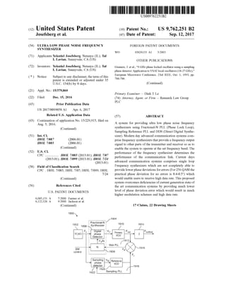
  • 13. U .S. Patent Sep. 12, 2017 Sheet 11 of 22 US 9,762,251 B2 1800 1802 1804 1806 1808 SW control Prinsen Fout FoutfinalDDS 7 FrequencyDigitalphase Frequency Detector Fp2 Primary VCO18 DDS clock 1810 Main PLL 18164 + 2 1814 1812 TFT for1820 rexoL2 phases???? VCO For Sampling V12 Referencephase VCOdetector SamplingPLL !1822 |18181818 1824 1822 L1824 FIG . 1819001900 1904w w 1902- 1910 1906100 Fractional-N Synthesizer 1914 wiewirim roxo Fo?cxo Digital VAVanDigital phase Detector FoutPrimary Fout outfinalPrimary VCO wwwwwwwwwwwwwwwFUN 7912 Main PLLN SW control CCCCCCCCCCCCCOLE www 1908. * * * * * * * * * Sampling Referencephase detector † 1920Sampling PLL1922 1918 FIG . 19
  • 14. U .S . Patent 2016 2002 ras 2004 SamplingPLL comb Comb SamplingVusDCswitchvel Loop phase generator detector filter TCXO VCO Sep. 12, 2017 2008 2006 Vid 2010 2012 No DigitalPLL mm DigitalPhaseFrequencyDetector 2018 Sheet 12 of 22 2014 FIG.20 US 9,762,251 B2
  • 15. 2102 2100 PHASENOISE(dBc/Hz] Ôägggaje? ?????????? Hummer 100 AP1396MB minin FIG.21nnnnnnnnnnnnnnnnnnnnnnnnnnnnnnnnnnnnnnnnnnnnnnnnn 1427MHz1 1K10k FREQUENCYOFFSET(Hz)100k1M NISSSSSSSSSSSSSSSSSSSSSSSSSSSSSSSSSSSSSSS nininnnnnnnnnnnnnnnnnnnnnnnnnnnnnnnnnnnnnnnnnnnnnn 1696MHZ Yooo wysymy w 10Minninnnnnnnnnnnnn meno H --2104nnnnnnnnnnnnnnnnnnnnnnnnnnnnnnnnnnnnnnnnnnnnnnnnnnnnnnnnnnnnnnnnnnnnnnnnnnn mene 100M 21122110-21082106 IST?79L*6SN77JOETJ??4SLIOT‘ZT`d?sbu?d'Sin
  • 16. FIG.22 US 9,762,251B2 #23? Frequency[Hz] 303 Z' ???? . 2-30 00 Z- 7-8 ff}} ZHf}{0;L ? ? ?f *}; ffiii;ii i. { } }{ }} } } } --06f }}}}} ? ? '3!:-:- ? ???|? ? ??'?? .?? ? ? ? ? ?f ??? ? ;_ ? ;_ ?????? ; ???:; ?{{ {{ { { {{{{{{{{{ 2214?? $ % $ # Sheet 14 of 22 -222 '??'? ????????? ???:;;:,?????????????????????????????????????????:;:; ??????????????????????????????????????????????????;: ?????????? ???????? }}}|.??{; ?????:'.?i ????????? ?????????? '!!?:}}} ???????1 www!!??????????????1 :%:??? ?????????????????????????? ????????????????????? ?? ???????????????????????????????????????????????????????????????? ???????????if ?????????????????????????????? ?????????????????1??????????|????????????????????????? ???????:;!???????????????????|.||????????????????????? ????????????:;;;:1????????????????????????'?"' ?????!!?! ????????'?!?????'? ???????????????i : i? ??|??'?-i----!???-)-----+--|??-'+?????????4-----++H-!-+-??????????????????:?????.-:4-------+-?-*-????+|??????- - A++H + - - ?????????:!?????????????????????????????????'_ ????????????????????| ???????? ??????????? ???????}}} ???????+?????;r - ff??????[--???????????????????????????;?????????;:??????? ???:;;;.;i????????|.?;??|?? ;;;;;;;? --- X : ? ; - f - - F --????? ?:fr ????????i????????? ????????? ?????????????????? ????????? '!!?:;;;i ????????? ???????? .!.!-:::?: ?;?!?:!.- .?.!!??:} ???????? !;fi. ??????????????????: ; ffy i : ?????????+ffffe ? ???????!?'!!!'''1 ??????????????????????????:;-;????:;_;?????:??????????????????? ????????????????????????? ????????? ????????????????? ?.?..........?... : -. .. i M.....?.??.:???i..??.......????..????.?.(.;.l???????????? ??? ??..L.-???????.????.........????.???} ????????????????????? ???????? ? ?????? ????????f ?????????????????'?????????;!;;;;????????????:;''.???????? ????????? ?????????!}}}}}}}??????????????:3 ??????}}} ????? -yr- fff---;;r;":":-' :;ff'ff *f;*- g *** f -; ;-i $;;f:" limam??? 2210 ??2202 ? PhaseNoise(dBc/Hz) ?? ?? - ?? ?.? ? ?????? ??????? ?? ????????&{??? ? { { { {{{{ ? _;_;_.; ?? ????????? -- -- 2238?? . ? ?| ? 2206 * ' ; ?????: ? } ?????:}?-.;..-..-..???????.-:.-.-........ _ Ser0.12,2017 ?; 1.?????? ?? ? ? ?????? ? ? ? ? ? ????? ? ? ? ? ?????? .-......... . L :}?.?.?.4.?...-.?....--!tit;.}.?.?..........??????.?..?-...f-.-.-.???????. ? ? ? ??????? ? ? ? ?????? ????? fgta } OF ??FutaP.???? ? ??? ??? ?????????????? ???? ?? ????????????????????? ??? ??? ????????????????????? ??? ??? ?????????????????????? ? ?? ?? ?? ???????????' ?? ?? ?????:;??????? A;; --- - ---- ? ? ;_ ???:;;_;_;_ ? ?????? .....????;:! ? |. ? ? ?????? ? ? ? ? ????? .??:;_;___.__-.;.....???????.. ? ? ?????? ? ? ? ????? ? ? ????? ???????? ??? _ i| !????i ? ? ..?? !..|......!???:??? i' ??????i i };.;:?i Filter ? - -- ?? ?? ? { {{{{{{{ - ????????? ??????????:;!???!f ??????:;????????? ???????? ?????:;'????????? ??????:i????????;????????? ????????? ????????? ??-'_i_::????? :--?-.????||?:1--------'-!;:????????:'!'.???.?????'_}£ ?????????????????????????????????????????????????????????????????????????????????????????????????????????????????????????????????????????????????????????????????????????????????????????????????????????- .? ?XTAL OM- AllNoiseContributors US. Patent ?00}22
  • 17. U .S . Patent 2300 AllNoiseContributors otowoween wwwb ili!!1 iL -- ili: 1 I! ? . . ! - I - - - - - - - N VCO???. PDFilterDivmom.TotalPLL . U?!! III - } liit liiii!} Sep. 12, 2017 Limmmmmmmmmmmmmmmmmmmmmmmmmmmmmmmmmmmmmly - + + ew - - ---- -- ! !! I -- .... i . 1 Milit - - - -- -- PhaseNoise(dBc/Hz] TotalOIP papapatay }primit 11111illiL11 1 ii lin Tiit liiiiii i111111* ::}liitI lip1Tf1!!11ii!iiti 1::11il ittiili111!!!ii!Ilir --S .Lil.-.-L-IIILJU----I--LLLL!!11--------- -- ! lif}I till111!!!!iiili !!ii! i ?lili :11 --- tit------† H------- ---------- iii} 1:}}}L{i}iirti !!!! i i !!ili1iliill !!!! iiIPIN1111ListItiliit ****1717***** 7:7 !iii!!!! !!111IIliini iii!!!!I iit!i!!!!} --ISLITI---L-LIIL L --- TUL-LILIII11C-LNIH 1:Ah!i1Interventioningangpapuntang1!111!iliistinei :} alarmantneilli II}!! 1}1illi*}}{:11 I:}liitwalilill!Iiilis: ·**of***-lampa-** **-*fosfor11111***-**17****** *itlayat11togofor""!**forInterior irayonutIlilin gawegestioniiPrima interesniLaweyan!!!!! bi:111 iii!! I111!! !Ilini nisl 1 !! :?liii}! }lill]111!! iNiliit kaupyti II!! - ?ji-iiiiiii?---7- --7-7MT--?Wit---?ir I!!!il{} }tilII!!!i Fit III !!! !!iiif}I11 1{11.!!!! 1111 VIII. {!!!!! -I.LL1.li.--LIIILIJU.. -LLII-andu_l_ lenrakkauttamann Biii! Lii!{}1111 liit! ! Lii!!!!i11listI till! !!!! INI! liit --------11----------ft!}-------- **------*111!--------ge-1 *** wwwwwwwwww www. a...à.... iniiniind n.2306 -1204 2302 - - -1304 -2308 - --2310-2310 - -1404-1504 -160 100HZ Sheet 15 of 22 - etScale).ExportPlaipa m23122312 1KHZ 10MHZ100MHZ 10KHZ100kroz1MHz Frequency(Hz) 2304 FIG.23 US 9,762,251 B2
  • 18. FIG.24 US 9,762,251B2 2404 Frequency[Hz] Hzfk ' Hz _ 10kflz _ 300kha { { ' Hz10 ' M ' Hz100MHz?100 ?70- ???????????????????????????????????????????????????????????????????????????????????????????????????????????????????????????????????????????????? ? ? ? ? ???? ? ?.- :1i'' ; -& 242??? -- -L .. .. ..? _Sheet16 of 22 Q-????2?? : ' ' ; ??:;; 24;2-- 2408 ? PhaseNoise(dBc/Hz) ?????????? ????????? ????????? ??????? ????????? ????????? ????????? !???????? ?:;!|||||??;_ ;!?:? ?????????????????? ? ?????| ??????????????????_?????????; ?????? { ff- ? ' ? - - - - - - - ' : ' fff - - - - - - ff; - - : - - f - - - - - ; ; - : : ; ; - - - - - - - { g 38 5 3 :QX - '}{??????????:33 ff:; ?????????????????? ??????????????;:3 ????????????? ???????:i?????????????????? ???????? ???:;i'} ???????? ???????????????????????????? ???????????????????? ???????? ??:; - - H T - - - ; : ; - i : ; 1 -?--?--:--;:?:rrr - - - . -- - - r ;.----;--;-;-?????;:---F--:-'-??????----????? ???????????????????????????? ?????????? ;;M;.::|?? ???????? ??????:; _f_?.????????????? ??.?;:; ????????!.?|??????? ??????????????????????????;%???_ } i_ ; ww! ; _ ' _ ; ?? :::-----?-?'?ri ?*:---?????':"-;";fif??????????????:;""'"'";-*F -' rT?:*-*???????"?'--;*---;"f " r';;; ????????i?:???????? ??????????? ??????????? ?????:i ????????? ???? ????? |.?????? ????? ????????? ??????????? ??????:???;_;_;_;Ii?? ????? ?|.-.-------i H . - . - . - ; -? F - ' -.'.--?--?--|?;-F-;.--???????----------????-.-.-.-*..-.--?--j - - f - i**--------..*-*** ???????????????????????????????????????""???????????????????????? ????????? ????????????????????????????? ???? ?????? ??????????????????????????:;???????????1?????||? ;i.--.???.??.14?????-i-;*-,--?????.-.|.????i.-???????-------??-.-.-,?-'?.;.;;----------j--?????,?????-.-..-..|??.???.--+--++1-4---------"*+-?.||? ???????????????????????:;;;;??????????????;!|? ?????? ?????????;_;_;_;?!;!????????? ?????!'; ??????? ??????????:_'{_}|?:??????????;;;!!(!?? ???????? ??????-???????????????????????????????????????????????????????????????|???+??-f??????????????????????|4? ????????? ????|?? ??????:;? ?????????? ????????? ???????? ???????:i????????? ????????? ???????? ??:;'f ' ij _ f l_?????? ???????:i ????????'_???????:; ????????? .????.???!??-?-J??1-!--!&i?????-!?-???????????.??????????1-?'-i - i??????????????3; ?????????????????? ???????????????? ???????|??????????_;;;;'}| f_'?????? ???????? ???????|??????:;.f??|.|??;; ????????????????'????????? ......;!,:.i.;!...?!.?!,'!,'... ...........!|;!!........??;:;.'i... ????????? ????????? ?????????.!f'.????????????;!|????????? ????????? ?????????????????????????????????!';???????? ????????? ????????? ??????????????;!|;???????? ????????????????????????????????????????????????????????? ?????????????????????????? ? 1..-..; | | –?! 22436 . ? .-.-.|. ????:;_;'_ ;'iifi_ .-00£- ?.?.?.?????? {2}O}----- c} Sep.12,2017 ? ? ? ? ???? ?_ ? ? ,???? ? . ?..?. . . .? ?? --.. d { € { Ob?? .--Mit? ...... ! |:!!| .......' Filter ????????????? ? ? SjoinquiuoaSIONIV ? X ' AL ? _2400 U.S. Patent
  • 19. US 9,762,25182 092? (ZH)Aguonbely ZHA{_ ?0 ZFHWN£ ZHf0f; £ _ ZHA ZHfVAN001 _ LHWNQ; { { { |!'{{{ ? ...09£ -0gt ?? ; ; ;:;;;_; ???? 3+...+ 11 111 11 1 * --------- ::: ?? . .;; ?? ????????????????????????????????????????? ???????????????????????????????. ?????.3.??.i.1????????????????????||???|???.?.?:???????????:L?????????????????????£???.???4 , 11.}?..?????.??????????; ?????????????????????????????????;:i_ ;.}}}} ;;_;'.?.'??.????????????????????????!? ????????????????????????? ??????? ????????????.???? ????|?|i|.????????? } }????? ???????}_ ???:;ff ??????? ?.?.?|';??????????????:;;.;}}}.????? ?.?.?????? ??????????????????????????????????? ???????? ??????.?.?.'.i , l|;.?.?.??.;,??....??£;&.???.???..?.??.??.;:££i£-..;.-..;?????|..|???..?.?.?;114 i??.?;-..??1...???????.:- ??????????????????? ????????? ????????????????????????:;° ???:;;__ ???????? ;_;_;;!|;;??????????????????? ???:??:'? ?????? ????????????1.IJ??.????????????????1?????????????????????????????????????-?'??????????????????????????????????????????????????????????? !.????????????????? }}???????????????? ???????????????????????:;] ;;,'?' ????????? }}}}}}'}}.!???????| : ?.?4 4???? ???????'? . ????? ?? ;.58 Sheet17 of 22 ?? ? ?? ?? ?? ???? 80-C { { { {{1!{{ ? { { |{{{{{ ??A. ? --- ºi ---L}}i;------II/{_L ---::__*_---- ? -1-----}_{{-- 1-*-----{{}}{{ i- -CQS ? ?? PhaseNoisefdcfdz ?9f392 ? ??'???? ????????????? ? };**ff|||. ?????? ;ffff.!!|. ?..??.|.3...,i . I?. ??? |?|????f 1????????? ?????????? ?????????????'???????????:;' ????????? 1.?}}}}}}?????:!???????????'_;_;} .????????????--????.1...........?.'...???.?.?--..??????…?.;; ? ??- ; ; ; ;;?? ! * *** * * * * * - ? ? ???? 882??? ??? ? ????????? ? ? ? ?? ?????? ?? ?? ???:; ?????? - +x-4 2 11 11 -11--244 -------- 1x1: --{x C{ --- -- ? - ????????????????????????????? AC-.....-. falf;-g -- {J ??? _ Ser0.12,2017 -;- ?? ????????????????????????????????????? ???????????????????????? ?????.?{{|??????????????????????????????? ??? ??????{il????????L.????????.?????-1??.?????????????????.??.???L ' f?????? ??????1;_??????????????????? ?? __}}}??' ||||||i??????????1??????????????:;' ????'???????????1??????…??? .?£?1|1???.-.!.-.-3 1?;L;---}..?.???.??Li-.--.?..??-f&;?J..? ???????????????????????????????????? }}}}}}}}????????????????||????????'_ ???????????????????????????????????????????????????????????? ????????????????????????? ? ?FWLX ???? -.- ?? ';;;;;;_;_; ? "f f? QQ';' ??? - ? * ???44?????????????????? ?????????? SjoinquuoaSIONIV 009/ US. Patent
  • 20. 905 US 9,762,25182 $-39 (zh)Aouonbang ?Z }} ?2 ??0}{g}}} }}}}}}} }{0 ?2 ;;; ???? -09£---08£- - --- -- {{{Hi ??? ?????????r?:????????????????????r?????????????????; ????????r ; - r?????????????????? -.??.-.;.?.-1..??.?1.........??.??..J.:*-.-..-..-.....,1-1-?.L . : ii........'-.-....?.?.-1:.-..-?..£.:.£££ * .|...?J.;]--).;; ?????????????????? ?|????f : i ???????|:?????????? ??????? ;_}|??????????????????????!?????:}| ?????????????}}}?????????????:;:; ??????? ????????-????.'1???????????????????????????????????????????'£??????????????????? ????????? ?????????????????????:;?!???????|??'__????? »«?????? ????????????????????????????????_'.}??????? ||?????? ?????????????:;?;?????:!'! 'P!;;.???? ?-HOCHYWO0X;:' - g-' ?? - ?-£-dgt? _f _i MJif| -------LiL - ***--- ----- - ---- -- i4------------- * ????????? } -- 4------ - -: :- ???}}}:!?????????????????: f ????"f fff|??????? .}|???????????????????????????????????1: |??????? ???????????????????????????????????i??? _ f i??:???| ;..1..I.??????;???.£????...'.,-1.3.3,?:.J........??..?A.|...?..?.:.. i A ( , ;............??? ;_;'';;;'????????????????????????? ?????????? ;_;'???????????????????????:;_!??4????????????? }}????1.;;???||||||???????????????????? ?????}}}???????? ?90£[???@809 Sheet18 of 22 -- - - ??… . . - 00Z --<--- 3:!------Fi{}{C ! ! ! t ... Crea. + --- LiL--- i!i;;;; ai------{{it--:-1-- L ! : + i ; Phrase'Maise[d8cffe }gc ?. --- - ---- ?. ? -- fed{€}{OL - ;? ? --- --- - -- { { ????????|.? _'.??????????????? ||?;;;?!;.)-f?????????:!!i_ |if |:1? ????????????????????????????????? }}}}}};1??????????????????????????? ?????.??..??????.???????.?????????????.?.????..??-.??????:???????.???.??.?.?.|?????.???.??.:-.-.-.-}}} ?????????;_ :?f : i ???????!; f_{_{|???????????????????i:????????]: ?????- f_;_???????????????????????!????:;': ?????8??????????????????????????????????????????????????????????????????????????????????????? f 1 1?????????????? ;?????? ???????1: ?||???????????????????:;? ????????? ??_||?????? ????????????????|? ?.????????I??????|?||????0??|?????????????????????????????.?????????.?1{ ??????????????????????????|i_{_!;;;|? ?????????????????? {_{|?????????????? ??????:1? ?-.,,-,.....-1.??.?.?......?..?..?.?.??.????.?.?...?..?.??.?.?.???.?...|?...?-.'..'..?.?:,I?.......4 ??????:1????????'???????????????': ????????????????????????i?: ?????|:|: ???????????????????????????????????????????????????????? ??????????????????????????????????????????? {{{{{{{ ?????????? ????????? 168ff-c ??????????????????????????????????? _ Ser0.12,2017 -- _} {{{{|} { { ;.;;:;.{{ ?- ??: ? . ?? V 'X' ?? : ::; ! ' COA sioinquiuoOSIONIV 009/ US. Patent
  • 21. FIG,27 US 9,762,25182 0 f- fedKatiefabels _LfjM}£ _ZX00} Z'HWW{ _LFH{00+ £f-H?{{ _Z'H'A'f}£ Z{{WAN00b -£?0 ? ? ? ? ? ? ? ? ? ? ? ? * - ? ? ? ??? ? ?. ?. ?? ?? ???????}} ????? ??? ????}_? .109£-3}= ?????? s 3x4k!}SEX3 ---2712 -{{ ;!.;;;_;** ' ????'; ?????? ?? ? ? ?? ????? ? -750! ? .- .- }}};|!M ??????? ???:}1 'Mff??? ???????????????? ????????????????? .........??????? ???????? ???????? ????? ?? ?? ?? ????? .? ? ' _Sheet19 Of 22 ???????| |||||; 2 / 02 ??? ????:;ri?? ? ?? ??? ???? PhaseNoise[dBc'Hz -2708 ????????? ???????? ????????? ???????? ????:;}} ???????????????????????????? ;:;??;.}}} ??????????????????!??.?????3 ?????????:.....????????.........??????....????;.??f:3 ???????? ???????? }}!??????? ??????:;;. ???????? ;|!???????????????? ???????????????????????????????????;; ???????? ??????????.. ???????? ???????? ???????? ?????????????????????i???? ?????????????????????????? ????????????? .?;.??????||;.??!??..?!!???????????????????...??????? ??????????!????????{_{_?????????????????? ????????? ???????|???????????????????? ??????????????????????????? ????????+C;:??????? ' ?????? '?.?.?.???? ??? ???:?? ????????'???????????????.????????-f??? ? }:;??}}}} fi???????-?******?????????; ?????????.|. ??????????????????????????? ????:;;;.?}} ??????? ??????????? ??????? ; !??????????????????; ???????? ??????????????????????????? ??????????????????????????????????? ........?..?????????????...?????????.,????????????.......?????4?? ????????? ????????? ??????:;? ????????? ????????????????????????????????????? ;????????? ??????????????????? ???!..?????? ......??????? ??? ;!??????? ????????????????????? ????????'_??????????????????????????? ?????????? ?????????????????? ???????? !??1?.?....?????????????????? ????????? ????????? ?????}}}!?????????;|!??????? ?????????????????? ?????????????????????? ???? ?? ???????????? ???? ???????}}?????????????????? ? ??????? ?????????? }};;??? ????????? ??????????? ?:?????? --!--.-----;---------.-.-.-:-..-.-.--?-- ?????????????? ??????? f??|?!; ?????????????????????????????????????????? 90&C ?? ??? ?????' ??? ;??? ?? . ?? ! { {{{{{{ foHENO----- Sep.12,2017 '... G}£- : ? ?????? ";' ;,:; ??? ??? ???????????????????????? ??????? ??:;?}}?????|.}???????????}}}?????????????? ??????????????????? ?????. !fc f - - 6 { { .{ {{{{{{ ? ? ? ? ?? ? ?.?.?.?.?? ? ? ? ? ? ? ????? ? ? ????? ? ???:;;_i_ ?| ;_ ?;: ? ????? ?????:?????? ; j !; {{{{{; ??? ??? ;_ 1_ ?!_ :_ ?_1_ :'??? Qij--Filter.PQ-XA AllNoiseContributors QQ'? 2700 U.S. Patent
  • 22. U .S . Patent 2800 Start AnUltraLowPhaseNoiseFrequency Synthesizercomprises2PLLS-1.Main PLL2.ReferenceSamplingPL Sep. 12, 2017 2802 TheReferenceSamplingPLLreceivesclocksignalsfromaTCXO,generatessamplingfrequenciestoeliminatedigitalphasedetectornoisefloorandforwardsthesamplingfrequenciestoa DownConvertMixer wwwmnnnnnnnn 2804 TheMainPLLreceivesclocksignalsfromalownoisefrequencygeneratorDDS,generatesoutputfrequenciesandforwardsthemtowardstheDownConvertMixer Sheet 20 of 22 annnnnnnnnnnnnnnnnnnnnnnnnn YYYYYYYYYYYYYYYYYYYYYY 2806 TheDownConvertMixerwhichisapartoftheMain PLL,receivesfrequenciescomingfromboththeMainPLLandtheReferenceSamplingPLL,mixesthemtoreduceamultiplicationnumberNtoachievehighdatarates,highmodulationschemesandlow sdfphasedeviationerrors. ( EndEnd ) FIG.28 US 9,762,251 B2
  • 23. 2900 U .S . Patent Start AnUltraLowphaseNoiseFrequency Synthesizercomprises2PLLS-1.Main PLL2.ReferenceSamplingPLL. Sep. 12,2017 W iiiiiiiiii 2902 2904 TheReferenceSamplingPLLreceivesclocksignalsfromaTCXO,generatessamplingfrequenciestoeliminatedigitalphasedetectornoisefloorandforwardsthesamplingfrequenciestoa DownConvertMixer TheMainPLLreceivesclocksignalsfromthesameTCXO,generatesoutputfrequenciesandforwardsthemtowardstheDownConvertMixer ???????????????????????????????????????????????????????????????????????????????????????????????????? ???????????????????????????????????????????????????????????????????????????????????????????????????????????? Sheet 21 of 22 wwwwwwwwwww 2906 TheDownConvertMixerwhichisapartoftheMain PLh,receivesfrequenciescomingfromboththeMainPLLandtheReferenceSamplingPLL,mixesthemtoreduceamultiplicationnumberNtoachievehighdatarates,highmodulationschemesandlow phasedeviationerrors. ( ? End ) FIG.29 US 9,762,251 B2
  • 24. U .S . Patent Sep. 12, 2017 Sheet 22 of 22 US 9,762,251 B2 3000 Start 3002ATCXO generates clock signals of low noise frequency ranges 100 MHz to 250 MHZ wwwwwwwwwwwwwwwwwwwwwwwwwww A SamplingPhase Detector receives the 1 3004clock signals and eliminate digitalnoise floor presentin the incoming clock signals 3006 A DigitalPLL is addedwith the Sampling PLL to improve performance and reliability ofan Ultra Low Phase Noise Frequency Synthesizer to achieve high data rates,high modulation schemesand low phase deviation errors. End FIG . 30
  • 25. US 9,762,251 B2 ULTRA LOW PHASE NOISE FREQUENCY Without the availability of the advanced state of the art SYNTHESIZER communication systems in today's markets like smart phones, it is not at all possible to access those high speed CROSS-REFERENCE TO RELATED data rates. One of the most important hardware element APPLICATIONS 5 present in those state of the art systems like smart phones, are frequency synthesizers. Frequency Synthesizers are a This application is a continuation of U .S.application Ser. major building block in almost every communication sys No. 15/229,915, filed Aug.5, 2016 ,which claimspriority to tems, such as advanced mobile communication systems U .S.ProvisionalPatentApplication No.62/181,221 filed on (LTE, LTE-Advanced), satellite communication systems, 10 radar communication systems and so on. Jun. 18, 2015. The entire disclosure of each ofthe above applications is incorporated herein by reference. An example frequency synthesizerprovides a frequency output signal to other parts of the transmitterand receiver so as to enable the system to operate at the set frequency band.FIELD The performance of the frequency synthesizer determines 15 the performance of the communication link. The mainEmbodiments of the present disclosure is generally important features of every synthesizer are: a ) Output fre related to systems to provide ultra low phase noise fre quency range,b)Outputfrequency resolution,c)Switchingquency synthesizer and in particular relate to systems to speed between channels and d ) Spectralpurity : Phasenoise,provide ultra low phase noise frequency synthesizer based spurious and harmonics etc .Amongst all those above men on using combination of Fractional-N PLL (Phase Lock 20 tioned features phase noise is the most important. The level Loop), Sampling Reference PLL and DDS (Direct Digital of phase noise determines themodulation schemethat can Synthesizer). be implemented in the system hardware and thus it deter mines the associated data rates and the communication BACKGROUND ranges ofthe systems. 25 If a communication system provides higher data rate the Wireless Communication Technologies have completely system is more efficient, and it takes less time to download revolutionized how millions ofpeoples in today's world are and upload data from the network. A higherdata transfer rate communicating to each other in a seamless manner. From can even save battery timebecause the transmission can be their early infantdays oflate 1800 's tilltoday the conceptof turned off much faster. A higher order modulation scheme wireless communicationshavematured beyond our wildest 30 implemented in the state of the art communication systems imaginations. Amongst all those technological advances enables those systems to push more information in the related to the field ofwireless communication technologies, wireless channels. However, themodulation scheme is lim the only thing which has remained constant is the applica- ited by phase noise. Hence to implement those higher tion of radio waves. On one hand radio waves can help us modulation schemes in the existing state of theart commu achieve communication between people who are located in 35 nication systems we need to reduce the phase noise. close proximity of few meters. In the samemanner in deep Mostmodern communication systems use sophisticated space radio communications those same radio waves can modulation schemes that are based on a combination of also help us achieve crystal clear communication between differentphases and amplitudes. The currentmostadvanced humans who are millions of kilometers away from each modulation scheme which is running in most of the smart other. 40 phones or tablets is 256 QAM (256 Quadrature Amplitude Wireless Communication Technologies have branched Modulation ). In this modulation scheme, the smallestphase into multiple different formats like Two-Way Radio Com - deviation for error (A $ ) theoretically is 3.7°. Practically, to munications, Satellite Communications, Infrared Commu- be on the safe side, it is desired to work with nicely lower nications,Mobile Communications,Microwave Communi- number. As 10 % is considered safe, hence the current cations, Wireless Data Communications, Wi-Fi, Bluetooth 45 generation of frequency synthesizers work with 0.40-0 .5º. Technology etc. Each and every single one of the above Thecurrent generation ofsingle loop frequency synthesizers disclosed wireless communication technologies have inherently does notenable to go to much lower phase error evolved tremendously and becomemuch more sophisticated due to phase noise. and state of the art. In this patent application we will The current generation ofadvanced state of the art com specifically dealwith systems associated with Mobile Com - 50 munication systems typically includes a front end module munications. and a System on Chip (SOC ). The frequency synthesizer is The evolution of mobile communication technologies part of the SoC and is implemented mostly in CMOS. The from their initial 16 (1 Generation) days of 1970 till 2016 front end module usually contains a low noise amplifier for which is today's high speed 4G (4 Generation )technologies the receiver, the power amplifier for the transmitter and have enriched human lives in differentshapes and sizes. The 55 some switch matrix . The SoC includes all the signal pro biggest impact which these gradual evolutions of mobile cessing elements along with the frequency synthesizers. communication technologies have brought into our lives is Currently the Wi-Fi and/or LTE synthesizers in the SoC set the humongous increase in data speed which has enabled the limit for the performance of the system . As a result, the seamless communications between millions of peoples. multi-billion dollarmarketremains at a technologicalstand Where 1G technology enabled communication systemsused 60 still. to provide us simple voice communications at only 10 Kbps Further, in many communication systems, Digital Pre data rate, the theoretical download data rate of the most Distortion (DPD ) is an algorithm that aims to pre-distort advanced mobile communication technologies as of 2016 transmitted signals in order to improve linearity. In practical which is LTE-Advanced (Long Term Evolution ) has been terms, itmeans that the transmitter is not completely linear proposed as 1 Gbps. This quantum jump in data rate from 10 65 and is distorting the signal. And thatbasically also prevents Kbps to 1 Gbps has left tremendous impact into common the system to be as effective as much as possible. So one peoples' lives. approach is to correct it isby using somealgorithmsto pre
  • 26. US 9,762,251 B2 distort the signal in the opposite way. To do this efficiently, (SOC )module. The ultra low phase noise frequency synthe the DPD algorithm requires the amplitude and phase data sizer is part of the SoC module. The ultra low phase noise about the transmitted data. frequency synthesizer comprises onemain PLL (Phase Lock Traditional radio systemseither utilize thereceivepath of Loop) and onereference sampling PLL. The ultra low phase the radio ora specialdown-conversion mechanism followed 5 noise frequency synthesizer comprises one single TCXO by a high-resolution analog to digital converter to capture (Temperature Compensated Crystal Oscillator) which pro the small non-linearities of the transmit path. The main vides input clock signals to both the main PLL and the problem with the above mechanism is that non-linearities reference sampling PLL . The main PLL further comprises and phase noise of the receive path or special down one Fractional-N Synthesizer chip, one primary VCO (Volt conversion path get added to the signal and the DPD 10 age Controlled Oscillator) and onedown convertmixer. Thealgorithm cannot separate the non -linearities and thephase Fractional-N Synthesizer chip includes one Digital Phasenoise generated and added during the down-conversion from Detector and one software controllable variable frequencythe ones thatwere actually created in the transmit path and divider. The reference sampling PLL comprises one samneed correction. The transmit path nonlinearities; can come from any 15 P15 pling PLL, and one reference VCO . This embodimentpro vides multiple improvements in system output which arecomponent such as low frequency amplifier, mixer, up converter,driveramplifier.Specifically the PowerAmplifier based on the following technical approaches— a) using of (PA ) is the main source of nonlinear distortions in the dualloop approach to reduce frequencymultiplication num transmitpath and the main goalofthe DPD algorithm is to ber,b)using ofsampling PLL to makeitsnoise contribution pre-distort this to achieve a cleaner signal. Asmentioned 20 negligible, c) instead of a DDS clock like in the previous above all the receive path nonlinearities are added to the embodiment, using of a high frequency TCXO clock to transmit path with no way to distinguish between the two. providehigh frequency inputto themain PLL ,and d ) using Hence, there is a need for a low phase noise frequency of a high frequency Fractional-N Synthesizer chip in the synthesizer that can overcome the problems of prior art, main PLL. enable higher modulation schemes and high data rate by 25 According to a third embodimentofthepresentdisclosure reducing phase noise , resolve the locking problem in the a system comprising one ultra low phase noise frequency sampling PLLs and minimize DPD distortions in received synthesizer is provided. The system ismade upwith a front signals. The target of the present disclosure is to enable endmodule , a display screen and one System on Chip (SoC ) much lower level of phase deviation for error (Aø)which module. The ultra low phase noise frequency synthesizer is should be in the range of 10 % of current designs,or 0.04° 30 partof theSoCmodule. The system comprisesone sampling and thus enablesmuch higher ordermodulation schemes and PLL (Phase Lock Loop ), which is one of themost important enables an efficient DPD algorithm . building blocks of an ultra low phase noise frequency synthesizer. The sampling PLL comprises one TCXO (Tem SUMMARY perature Compensated CrystalOscillator),one CombGen 35 erator, one Sampling Phase Detector, one DC switch , one The present disclosure is discussed in reference to state of Loop Filter, one VCO (Voltage Controlled Oscillator) and the artwireless communication systems (smart phones) for one DigitalSynthesizer. In this embodiment, the loop filter exemplary purposes only. It is contemplated that the present is just a loop filter. The Digital Synthesizer acts as a phase disclosure is applicable to any state of the art wireless detector when the loop is locked and asa frequency detector communication systemswhich enables consumers to com - 40 when the loop is open, forcing the loop to lock from any municate with each other in a seamless manner. distancebetween the two frequencies. The loop will lock by According to a first embodimentofthe presentdisclosure the Digital Synthesizer.Once itis locked, the lock indicator a system comprising one ultra low phase noise frequency will switch the PLL to thesampling PLL while keeping the synthesizer is provided. The system is madeup with a front same control voltage, thuskeeping the loop locked. endmodule, a display screen and one System on Chip (SOC ) 45 The preceding is a simplified summary to provide an module. The ultra low phase noise frequency synthesizer is understanding ofsome aspects of embodiments of the pres partofthe SoC module. The ultra low phase noise frequency ent disclosure. This summary is neither an extensive nor synthesizer comprises onemain PLL (PhaseLock Loop)and exhaustiveoverview ofthepresentdisclosure and its various onereference sampling PLL. Themain PLL comprises one embodiments. The summary presents selected concepts of high frequency DDS (Direct DigitalSynthesizer), one Digi- 50 the embodiments of the present disclosure in a simplified tal Phase Frequency Detector, one main VCO (Voltage form as an introduction to the more detailed description Controlled Oscillator), one frequency divider and one down presented below .Aswillbe appreciated,other embodiments convertmixer. The reference sampling PLL comprises one of the present disclosure are possible utilizing, alone or in TCXO (Temperature Compensated CrystalOscillator), one combination, one ormore ofthe features set forth above or sampling phase detector, and one reference VCO. This 55 described in detailbelow . embodiment provides multiple improvements in system output which are based on the following technical BRIEF DESCRIPTION OF THE DRAWINGS approaches— a ) using of dual loop approach to reduce frequencymultiplication number, b) using of sampling PLL The above and still further features and advantages of as the reference PLL to make its noise contribution negli- 60 embodiments of the present invention willbecome apparent gible, c) usingofDDSto provide high frequency inputto the upon consideration of the following detailed description of main PLL and d) using of high frequency Digital Phase embodiments thereof, especially when taken in conjunction Frequency Detector in themain PLL. with the accompanying drawings, and wherein : According to a second embodimentof the presentdisclo - FIG . 1 illustrates a general block diagram of a negative sure a system comprising one ultra low phase noise fre- 65 feedback system ; quency synthesizer is provided. The system is made up with FIG . 2 illustrates a generalblock diagram of a standard a frontendmodule, a display screen andone System on Chip Phase Lock Loop (PLL); en
  • 27. US 9,762,251 B2 FIG . 3 illustratesa simplified drawing ofa digital phase generating input frequenciesof250MHz in accordance with frequency detector; the second embodiment of the present disclosure; FIG . 4 illustrates an example ofan active filter as applied FIG . 28 illustrates a flow chart depicting the operational to a general PLL; method steps of the first embodiment; FIG . 5 illustrates theprinciple of sample-and-holdmecha- 5 FIG . 29 illustrates a flow chart depicting the operational nism ; method steps of the second embodiment; and FIG . 6 illustrates a schematic of the step recovery diode FIG . 30 illustrates a flow chart depicting the operational as comb generator feedingthe dual schottky diode that acts method steps ofthethird embodiment. as phase detector; To facilitate understanding, like reference numerals have FIG . 7 illustrates a complete example schematic of the 10 been used,where possible, to designate like elements com comb generator and sampling phase detector with RF pre- mon to the figures. amplifier and two DC buffers following the phase detector; FIG . 8 illustrates a 64 QAM modulation scheme used in DETAILED DESCRIPTION communication equipment; FIG . 9 illustrates a phase noise plotof an example free 15 Asused throughout this application, the word “may” is running Voltage ControlOscillator (VCO ) in the frequency used in a permissive sense (i.e.,meaning having the poten domain (spectrum analyzer),withoutbeing locked in a PLL ; tial to ),rather than themandatory sense (i.e.,meaningmust). FIG . 10 illustrates a phase noise plot of an example Similarly, the words “include”, “including” ,and “ includes” Voltage Control Oscillator (VCO ) in the frequency domain mean including but not limited to. (spectrum analyzer),compensated by being locked in a PLL; 20 The phrasesatleastone“,one ormore”,and “and/or” are FIG . 11 illustrates two plots: (a ) a simulation of phase open-ended expressions that are both conjunctive and dis noise of an example PLL , and (b ) is an actualmeasurement; junctive in operation. For example, each of the expressions FIG .12 illustrates aphase noise plotofa closed loopPLL, at least one of A, B and C", at leastoneofA , B,or C",one showing clearly the effect of the phase detectormultiplica ormore of A , B , and C " , one ormore of A , B , or C " and " A . tion number 20* LOG (N ) within loop bandwidth ; 25 B , and/or C ” means A alone, B alone, C alone, A and B FIG . 13 illustrates a plot ofmeasurement terms of phase together, A and C together, B and C together,or A , B and C noise in 1 Hz bandwidth at a Afoffset frequency from the together. carrier. The term " a" or " an" entity refers to one ormore of that FIG . 14 illustrates a generalblock diagram ofan example entity . As such, the terms" a " (or " an" ), " one or more" and dual loop PLL; 30 " at least one” can be used interchangeably herein . It is also FIG . 15 illustrates a generalblock diagram of an example to be noted that the terms " comprising”, “including”, and dual sampling PLL; “ having" can be used interchangeably. FIG . 16 illustrates how impulse or "comb” generator The term “automatic” and variations thereof, as used changes a wave shapeof a signal from sinewave to pulses; herein, refers to any process or operation done without FIG . 17 illustrates an example outputof a comb generator 35 material human input when the process or operation is in the frequency domain; performed. However, a process or operation can be auto FIG . 18 illustrates a block diagram of an ultra-low phase matic, even though performance of the process or operation noise frequency synthesizer as suggested in a first embodi- uses material or immaterial human input, if the input is ment; received before performance of the process or operation. FIG . 19 illustrates a block diagram ofan ultra-low phase 40 Human input is deemed to bematerialif such input influ noise frequency synthesizer as suggested in a second ences how the process or operation will be performed. embodiment; Human input that consents to the performance oftheprocess FIG . 20 illustrates a block diagram ofthe sampling PLL or operation is not deemed to be “material”. system as suggested in a third embodiment; FIG . 1 illustrates a generalblock diagram of a negative FIG . 21 illustrates a phase noise simulation plot contrib - 45 feedback system 100. uted by a DDS chip in accordancewith the first embodiment The negative feedback system 100 hasan input R and an of the presentdisclosure; outputC , a summer/comparator 102, a forward path function FIG . 22 illustrates a phase noise simulation plot contrib G 104 and a feedback path function H 106. The summer/ uted by amain PLL in accordance with the first embodiment comparator 102 compares the input R with a sample B of the of the present disclosure; 50 output C fed back through function H 106 , to produce an FIG . 23 illustrates a phase noise simulation plot contrib - error signal E that is relative to the difference between the uted by a reference sampling PLL having the TCXO clock inputR and the feedback sample B . This error signalE isfed generating inputfrequenciesof 100MHzin accordancewith to themain element G function 104 in the forward path . If the first embodiment of the present disclosure; the output signal C tends to drift upwards, the error signal E FIG . 24 illustrates a phase noise simulation plot contrib - 55 pushes it back downwards and vice versa. Thus, thenegative uted by a reference sampling PLL having the TCXO clock feedback system 100 stabilizes the output signal C . The generating inputfrequenciesof250MHzin accordance with negative feedback system 100 finds applications in many the first embodimentof the presentdisclosure; systems for stabilizing frequency, output power, and many FIG . 25 illustrates a phase noise simulation plot contrib - other functions. uted by a main PLL in accordance with the second embodi- 60 FIG . 2 illustrates a generalblock diagram ofa standard mentof the present disclosure; Phase Lock Loop (PLL) 200. FIG . 26 illustrates a phase noise simulation plot contrib - The PLL 200 is a frequency feedback system comprising uted by a reference sampling PLL having the TCXO clock a reference clock 202, a digital phase/frequency detector generating inputfrequencies of 100MHzin accordance with (PFD ) 204, a loop filter206,a Voltage Controlled Oscillator the second embodimentof the presentdisclosure; 65 (VCO ) 208, and a frequency divider 210. FIG . 27 illustrates a phase noise simulation plot contrib - The VCO 208 is the main output block in the forward uted by a reference sampling PLL having the TCXO clock path, and is tuned to produce a frequency as set by a tuned m liment
  • 28. US 9,762,251 B2 480 V circuit.The VCO 208 has a frequency outputFout thatcan be frequency 1 MHz, then every time the division number N changed by a control voltage V , over a pre-set range of changesby steps of 1, the output frequency Foutchangesby frequencies. equalsteps of 1MHz. Thephase detector 204 is a comparator forboth the clock Like all negative feedback systems, the PLL 200 has a input Fclock and the feedback sample from the output Fout 5 loop bandwidth set by the componentparameters and the divided by divider N 210. The phasedetector 204 compares loop filter 206.In otherwords,thePLL 200 is a sophisticated the two inputfrequencies Fclock and Fou /N .When the two frequency multiplier with a built-in narrowband,automati input frequencies are not equal, the device 204 acts as a cally tuned band-pass filter as the output frequency Fout is frequency discriminator and produces either a negative or basically Fclock multiplied by the number N . The loop positive voltage,dependingon the polarity ofthe frequency bandwidth is also responsible directly for how fast the difference between the two inputs. When the two input output frequency of PLL 200may change between different frequencies are the device produces an error voltage V/ frequencies. ThePLL 200 is a device where the VCO 208 is relative to the phase difference between the two equal locked to a single clock reference signalwhich is very low frequencies. butalsovery clean andvery stable and the outputfrequency The loop filter 206 filters and integrates the error signal can be changed by equivalent steps by controlling the produced by the phase detector 204 and feedsit to the VCO frequency divider 210 in the feedback loop. 208. The loop filter 206 is usually based on passive com - FIG . 3 illustrates a simplified drawing ofa digital phasel ponents like resistors and capacitors,but also in somecases frequency detector 204. it is a combination ofactivedeviceslikeoperationalampli- 20 phase detector or phase comparator is a frequency fier and passive components. mixer, analog multiplier or logic circuit that generates a The reference clock 202 is in general a low frequency voltage signal which represents the difference in phase crystaloscillatorsignalsource that feeds Fclock to the phase between two signal inputs. It is an essential element of the detector 204,and to which theoutputsignalFouis “ locked”. phase-locked loop (PLL ). A specialized variant that addi The reference clock 202 is set at some frequency for 25 tionally detects frequency is referred as Phase Frequency example a standard frequency 10 MHz Thelocking “mecha- Detector (PFD ). A phase-frequency detector is an asynchro nism ” transfers someof the qualities ofthe reference clock nous sequential logic circuit which determineswhich ofthe 202 to themain outputsignal Fout.Itsmain features usually two signalshas a zero-crossing earlier ormoreoften.Whenare: a ) frequency stability over temperature generally in used in a PLL application, lock can be achieved even whentherange of0.1-5ppm (partspermillion),b )accuracy- Can 30 it is off frequency. Such a detector has the advantage ofbe tuned to very high accuracy, c ) very low phase noise Its producing an output even when the two signals beingphase noise is transferred to the output signalmultiplied by the ratio of 20*LOG (N ) where N is the ratio between the compared differ not only in phase but in frequency. output frequency and the clock frequency applied to the The phase/frequency detector 204 compares two input phase detector 204. frequenciesFclock and Fou /N . When the two inputfrequen The frequency divider 210 is based on digitaldevices like cies are not equal, it acts as a frequency detector and gates and flip -flops, through which the inputfrequency F . produces one or zeros to produce a voltage control V , that is divided by a number N to produce F N which is fed to pushes corresponding VCO 208 in the direction of the the other inputof the phase detector 204. This number N is reference. In other words, if the VCO 208 is above the software controllable. The control signal comes usually 40 reference then the voltage controlV, ishigh to push the VCO from a micro controller or from a PC or from anywhere that 208 down and vice versa. When the two input frequencies basicallywill send software controlto the frequency divider are the same and a frequency lock is achieved, the phase 210 to change the division number N . The target of the detector 204 acts as a phase detectorand compares the two division number N is to enable the output frequency of the phases, and continues to produce an error voltage to control frequency divider 210 to be equal to the clock frequency of 45 the frequency and phase of the output device. the reference clock 202 FIG . 4 illustrates an example of an active filteras applied The entire operational procedures of a standard Phase to a general PLL 400. Lock Loop (PLL) 200 is as follows: If an inputclock signal Thekind of loop filteri.e.passive filter or active filtercan Fcock is applied, usually by a reference clock 202, the phase be chosen on the basis of specific requirement. A passive detector 204 compares the phase and frequency of the input 50 loop filter is based on resistors and capacitors only, while an signalFlock with that of the VCO 208 divided by N , and active loop filter is based on an amplifier and a capacitor generates an error voltage V ,that is related to thedifference resistornetwork in the feedback system . A passive filter is in the two signals. The error voltage V, is then filtered and preferred in cases where, a reference PLL is of a single applied to the controlof the VCO 208, thereby varying the frequency and willneed only a single voltage in order to stay VCO 208 frequency in a direction thatreduces the frequency 55 in that single frequency. The other reasonsbeing simplicity, differencebetween the two signals. When the frequencies of cost and most advantageously no addition ofnoise, asactive the two signals become sufficiently close, the feedback devices tend to add additional noise in the system .However, nature of the system causes the system to lock with the active filters findmore acceptances because ofthepossibil incoming signal. Once in lock the VCO 208 frequency ity of amplification of the input signal. Amplification is divided by N is identicalwith the input signalFort, except 60 made possible by an operational amplifier employed in the for a finite phase difference which is necessary to generate active filter. the corrective error voltage V , to shift the VCO 208 fre The loop filter 206 of FIG . 2, is an active filter that quency to the inputsignalfrequency Fclock, thuskeeping the includes an operational amplifier 402and a capacitor-resis system in lock . tornetwork 404 in the feedback loop. In someinstances, the Any time, the division number N is changed , say for 65 phase detector 204 ofthe PLL 200 may produce voltage up example by 1,the output frequency Fout jumpsexactly by a to 5 volts but the corresponding VCO 208 may need a step. In an example, if the reference clock 202 generates a voltage of above 5 volts,say, forexample, up to 18 volts in
  • 29. US 9,762,251 B2 10 order to reach its complete range, so the active filter 206 This type of product may contain some" search mecha facilitatesnot only filtering but also provides the capability nism ” to help lock thePLL . Themostcommon one involves to go to higher voltages. a positive feedback on the loop filter itself. While the loop FIG .5 illustratesthe principle ofsample-and-holdmecha is not locked,the loop filter acts as a very low frequency nism 500. 5 oscillator that drives the VCO back and forth across the The first sample and hold circuit 502 includes a switch S frequency range. When it passes close enough to the har and a hold capacitor Cy. The operation of the switch S is monic of the clock, it will lock and stay locked. A nicecontrolled by the sample control. When the switch S is feature of thismechanism is that it turns off automaticallyclosed, a voltage sample of the input frequency is sampled when theloop locks. This happens because ofthe nature of and when theswitch is opened,the voltagesample isheld on 10 the loop as a negative feedback system .thehold capacitor Ch However, this type of search mechanism suffers fromThe second sample and hold circuit 504 includes two buffersA1and A2with unity gain for isolation purposes, in many problems, its operation is subject to temperature addition to the switch S and the hold capacitor Cy. The changes and itmakes this product difficult to produce, tune bufferA2 is preferably an electronic buffer, so that thehold 15 andhold 15 and sell successfully. capacitor Cy does not discharge parasitically between con FIG . 800 illustrates a 64 QAM modulation scheme used secutive samples. In other words, the hold capacitor Cu in communication equipment. holds the voltage between samples. Communication equipment, including different smart FIG . 6 illustrates an example ofpractical implementation phones or tablets use a modulation schemecalled Quadra of a comb generator and sampling phase detector. The 20 ture Amplitude Modulation (QAM ). The QAM number schematic shows a Step Recovery Diode (SRD) as comb defines the amountofpoints on a 2 dimensional chart that generator feeding thedual schottkydiode that acts as phase thatisalwaysthe size of1x1. Themore points,the largerthe detector. density ofthe points. Thesignal has to be very clean for the The implementation circuit 600 including a Step Recov points tobe exactly where they are supposed to be so thatthe ery Diode (SRD ) 602 as a comb generator and the dual 25 modem can decide easily. Phase noise is one of the bottle schottky diodes 604 and 606 as a phase detector. necks thatlimit the data throughput.Ata system level,phase The inputto the circuit 600 in this example is a clock input noise is a statisticalparameter thatmoves amodulation point of 100 MHzsinewave. The SRD 602 is a special device that along a curve just as a vectorwouldmove if itpowerwould turns the 100 MHz sine wave input into a very narrow pulse stay the samebut the angle changes. If a certain modulation train of the same frequency, so it acts as a comb generator. 30 pointmoves too much on this curve, themodem will have The two schottky diodes604, 606 actas switches and actas a difficult time deciding where this pointbelongs and will sampling switches. The RF voltage (output from corre- flag an error. sponding VCO ) to be sampled is connected to a point In the QAM , delta o or delta phase is themaximum error between the twodiodes 604 and 606. The SRD 602 creates in degrees thatis allowed to demodulate the data correctly. an output of positive and negative pulses. Thepositive and 35 If thepointmovesby a phase ofdelta 0 , itwillbe understood negative pulses act as control signals to the diodes 604 and as a different point and in time the modulation schemeof 606 that act like switches. The sampled voltageoutputis an coursewillhave lot of errors. The 256 QAM allowsa phase errorDC voltage which is created by sampling theRF input error ofapproximately 3 degrees in order to understand the through the dualschottky diodes604 and 606. The outputof data and the 64 QAM allows a phase error ofapproximately the RF signalis sampled whenever the diodes604 and 606 40 7 degrees. By getting a better angle between 2 separate are opened by the narrow pulses coming from the SRD 602. signals,one can achieve a much bettermore information per The voltage sample is held on the capacitors C following the Hz, and a much higher data rate in modulation schemes, diodes 604 and 606. which can be very beneficial inmanyways even improving FIG . 700 illustrates a schematic ofthe comb generatorand battery life. sampling phase detectorwith a clock pre-amplifier and two 45 With our proposed ultra-low phase noise frequency syn DC buffers following the phase detector. thesizers, the improved phase noise translated to degrees is The voltage samples areheld on two very smallcapacitors better than 0 .04 degrees, which when basically translated to (which are basically the input capacitance of the voltage modulation scheme can facilitate much higher modulation buffers, no need for external capacitors) on both sidesofthe range. In other words, the points on the graph 800 can be dual diode pair, so as not to enable the whole capacitor to 50 much more crowded because there would be much more discharge parasitically between the samples. These capaci- points in highermodulation level. The points may be much tors are buffered by a couple ofultra -low inputbias current more crowded butif thephase noise ismuch better, it would buffers to prevent discharge between samples. The two be easy to distinguish between them without having prob voltages are summed, fed to a loop filter,whereby the clean lems of phase noise. With better phase noise, one may be V , is fed to the VCO to control the frequency 55 able to push more information perHz. On the samechannel, This implementation of sampling phase detector creates one can getmore information encoded and decoded. And an analog phase detector,very similar to a mixer. The analog basically it means that one can getbetter data rate. sampling phase detector has a certain defined locking space FIG . 9 illustrates a phase noise plot 900 of an example or locking distance, andit doesnotlock from any frequency free running Voltage Control Oscillator (VCO) in the fre difference like the phase/frequency digital detector. It has 60 quency domain (spectrum analyzer), withoutbeing locked in some locking range and only within that locking range, the a PLL . VCO locksby itselfon thereference. In a samplingPLL, the Assaidbefore,Phase noise is a key element in many RF VCO does not lock on the reference, but on the Nth and radio communications systems as it can significantly harmonic of the reference. In other words, one can lock a 9 affect the performance of systems. Phase noise is the fre GHzon the 90th harmonic ofthe 100 Megahertz clock. This 65 quency domain representation of rapid, short-term , random is doneas the input frequency is sampled every 100 cycles, fluctuations in the phase of a waveform , caused by time not every cycle. domain instabilities also referred to as “ jitter”.
  • 30. US 9,762,251 B2 11 For example, in frequency domain , where the scales are detectormultipliedbythatratio . The actualmeasurement of amplitude vs. frequency, ideally a frequency of 100 MHz phase noise ofan example PLL is illustrated in FIG . 11 (b). may look like a single line staying at exactly 100 MHz. One can see clearly the similarity between the two curves. However,practically with modern equipment in the labora FIG . 12 illustrates a phasenoise plot 1200 ofa closed loop tory,amplitude vs frequencymay not look like a single line 5 PLL, showing clearly the effect of thephase detectormul but it will look like a single line with a " skirt” 902 which tiplication number 20 *LOG (N ) within loop bandwidth. The goes wider and wider as we go down. The phase noise plot phase noise plot800 illustratesphase noises on both sides of 900 looks like theskirt 902 on the left and the rightofthe the carrier frequency fo, where the left side is a mirroredexactdesired frequency f . The quality, height,width ofthe image oftherightside. The phase noisesonboth sides oftheskirt 902 determines how the phase noise may affect the 10 cmcarrier f, looks like it is passing through a band-pass filter.system or theperformance of the system . So, it is desirable As illustrated, on both sides, the in -band phase noiseto minimize phase noise as much aspossible is to improve inside the loop bandwidth is flat in shape and is equalto thethe system performance. phase detectorand/or the reference clock noise multiplied by Phase noise is another term to describe short-term fre 20 log N . Atthepoint of the loop bandwidth, the phase noisequency stability. The signal generated by a frequency source 15 isnever practically “clean”.Its frequency isneverabsolutely goes up before goingdown again. This is due to addition of stable at the desired value. It has “Phase Noise” which is 3 dB due to a combination ofphase noiseofthe free running frequency shifting, i.e. small frequency shifts at different VCO and the phase detector. The upper straight line 1202 rates and different amplitudes of the main frequency. It depicts a phase noise contributed by the phase detectoratN1 changesaround the center set frequency f, at different rates 20 and the lower straight line 1204 depicts a phase noise and amplitudes. In time domain, the phase noise may be contributed by the phase detectoratN2. It can be seen that, referred to as jitter. Long term frequency stability is drift of there is difference in phase noise in the flat area, due to two the center frequency over timeor over temperature. different “N ” numbers. The phase detector contributes a FIG . 10 illustrates a phase noise plot 1000 ofan example higher in -band phase noise at a higher value of N . Voltage Control Oscillator (VCO ) in the frequency domain 25 Thus, in order to achieve low phase noise, it is essential (spectrum analyzer), compensatedby beinglocked in a PLL . to : a ) choose components such as phase detector and refer The upper line 1004 is the free running CO phase noise, ence clock with the lowest inherent phase noise possible, before it is locked in a PLL, and the lower line 1002 is the and b ) lower the ratio number N asmuch as possible. shaped VCO phase noise. In the PLL, the principle of FIG . 13 UlusFIG . 13 illustrates a plot 1300 ofmeasurementterms oflocking the VCO to a reference frequency attenuates the 30 nme 30 phase noise in 1 Hz bandwidth at an Afoffset frequencyphase noise of the VCO, in an amount related to the loop from the carrier.bandwidth . Outside the loop bandwidth , the VCO noise The phase noise expression is usually in dBc, i.e. dBremains almost sameas the phase noise without the PLL, while inside loop bandwidth it is attenuated more andmore relative to the carrier c powerlevelPs, in other words how asoffset frequency from themain carrier is reduced. Atvery 3525 low it is compared to the carrier per Hz, in a bandwidth of 1 Hz. That is basically the term that is used for phase noise ,high frequency, i.e. above the loop bandwidth, the locking almost has no effect, asthe phase detector correction signal dBcper Hertz (dBc/Hz) at a certain Af from the carrier. is not fast enough to reach the VCO forvery fast changes or Asan example forthe measurementmethod,suppose AF very fast disturbances.However, inside the loop bandwidth is 10 KHz, the phase noise power level Pss is measured at or at low frequencies, the compensated phase noise of the 40 the level of -70 dBm on the spectrum analyzer, and the VCO is much lower than thatof the free running VCO. All carrier power level Ps is measured at the level of 10 dBm , the frequencies that is closeto the center ofthe frequency f. theratio between the Ps 10 dBm and the PssB -70 dBm at are easy to detect and compensate. 10 KHz from the carrier is therefore 80 dB, so the phase FIG . 11 illustrates two plots 1100: (a ) a simulation of noise at 10 KHz offset from carrier and is -80 dBc/Hz. phase noise ofan example PLL , and (b ) an actualmeasure- 45 Formany systems, the important parameter to evaluate ment. performance is not the phase noise measured at a single FIG . 11 (a ) illustrates a simulation graph of phase noise frequency offset from the carrier, but the integrated phase ofan example PLL. The simulation graph shows the overall noise from one offset frequency to another one. Following phasenoise ofthe example PLL and includes the contribu are four different equations and terms to define integrated tionofall the components thatcontribute to the phase noise. 50 nphasenoise:The simulation graph illustrates first, second and third regions 1102, 1104 and 1106 of the phase noise. The first region 1102 which is very close to thecarrierdepicts a steep JL(f)df Integrated single sideband phase noise. linewhich basically comes from the reference clock such as (dBc) the Temperature Controlled Crystal Oscillator (TCXO , or 55 Sphilf) = (180/ ) . V2 ·|L (f)df Spectraldensity ofphase modulation, also known as RMS phase error.any other reference clock device). The first region depicts (degrees) the noise ofthe TCXO,multiplied by 20 log N , where N is Smu(t) =V2.5L(f)·fdf Spectraldensity of frequency fluc the ratio of output frequency to the clock frequency. The tuations,also known as RMS frequency second region 1104 depicts a flat phase noise which is error orresidual FM . (Hz) basically the noise floor of the digital phase detector mul- 60 Sy(t) = $nu(I)Iose Spectraldensity of fractionalfrequency fluctuations. tiplied by the sameratio of 20 log N . The third region 1106 depicts a steep line which is the inherent VCO phase noise not affected by the loop bandwidth and locking phenom Forexample, the first equation definesthe Phase Noise in enon. The dashed line 1108 depicts the VCO “ corrected” dBc. It can be translated by the 2nd equation to degrees phase noise inside loop bandwidth . Below the flat area, the 65 (relevant in respectoflearningmodulation schemes).As per compensated VCO phase noise does not affect the overall further equations, the phase noise can also be translated in result because it is way below the noise floor of the phase termsof Hz and timedomain phase jitter seconds.
  • 31. 14 out clo US 9,762,251 B2 13 FIG . 14 illustrates a generalblock diagram 1400 of an provides it to the VCO 1510 to control the VCO frequency example dualloop PLL. Themain target ofthe dual loop Fout. Fout=Fclock*N ,where N is the Nth spectral harmonic design is to reduce the number N . line in the “comb” spectrum . The dual loop PLL 1400 includes an upper PLL 1402, FIG . 16 illustrates how the impulse or “ comb” generator referred to as a main PLL 1402, and a lower PLL 1404, 5 1504 changes a wave shape of a signal from sine wave 1602 referred to as a reference PLL 1404, a TCXO 1406 operating to narrow pulses 1604. A frequency source 1606 generates as a master clock, feeding a clock signal F . to both the the input sinewave 1602 of frequency F1 and timeperiodprimary PLL 1402 and the reference PLL 1404. T1. The reference PLL 1404 includes a first phase detector The comb generator 1504 turns the inputsine wave 16021414,and a single frequency first VCO 1416 thatoperatesat 10 +to a series ofvery narrow pulses 1604 with sametimeperioda reference frequency F, The reference frequency F, is fed T1, and a pulse bandwidth as t, in the time domain . Forto a first input of a down convertmixer 1412. The main PLL 1402 includes a second phase detector example, if the frequency of input sine wave 1602 is 100 1408 and a second VCO 1410 that generates an output MHz, then the impulse train generator 1504 generates a frequency range F1 to Fz. A sample of theoutput frequency 15 seri15 series of very sharp narrow pulses 1604 of the same fre range F , to F , is fed to the second input of thedown convert quency. mixer 1412 and mixed with a single reference frequency F . FIG . 17 illustrates an example output 1700 of a comb The output from the down convertmixer 1412 is at amuch generator 1504 in the frequency domain . lower frequency (F?to F2)-F , This lowered frequency is fed In the frequency domain (spectrum analyzer screen), the back to the second phase detector 1408 through a frequency 20 output 1700 of the comb generator 1504 looks like a divider 1418 of value N1. " comb”, i.e. a row of lines extending up to very high Therefore: a ) Withoutthe down convertmixer 1412: F , to frequency. In theory, if thebandwidth of the clock pulse is Fz=NxFc, b) With the down convertmixer 1412: (F, to infinitesimal, the row oflines appear with equalamplitude F ,)- F ,=N1?F . As a result there is a reduction in thenumber to infinity. The output 1700 looks like a series of lines, with N :N1/N =((F? to F2)- F,)/(F , to F2). 25 the spacing between the lines sameas the initial frequency. The N1number isbasically the division number that the In an example, ifthe initialfrequency is 1GHz,thespectrum frequency divider 1418 will use to divide the output of the of lines is 1 GHz apart. mixer 1412 and feed to the second phase detector 1408. The FIG . 18 illustrates a block diagram 1800 of an ultra-low value ofN1 is setasminimal, as the output from the mixer phase noise frequency synthesizer as suggested in a first 1412 is at a much lower frequency than original frequency 30 embodiment. range F, to F2. The ultra-low phase noise frequency synthesizer 1800 To give an example: a) Suppose F = 1 MHz,b ) Suppose includes two Phase Lock Loops(PLLs).One is amain PLL F to Fx=10,000 to 11,000 MHz. Then N = 10,000 to 11,000. 1810 and the other one is a sampling PLL 1818. Themain Now If F, = 9000 MHz, then ((F , - F , - F ,)= 1000 to 2000 PLL 1810 comprises of a high frequency low noise Direct MHz. Then N1= 1000 to 2000. Thus, the value of N is 35 Digital Synthesizer (DDS) 1802 to generate at least one reduced from 11,000 to 2000. In dB , it is a ratio of 15 dB. clock signal Fc of variable frequency range. The high Thismeans,thatthe phasenoise is reduced by a factorof15 frequency low noise DDS 1802 generates the at least one dB. clock signalF of variable frequency rangeby taking input The disadvantage ofthe example dualloop design is that from at least one software controllable instructions and at while nicely reducing the number N in the main PLL, the 40 leastoneDDS clock signal. The frequency ofthe at leastone reference PLL ,containing a digital phase/frequency detector clock signal F is always lower than the frequency of the at becomes the main factor contributing to the overall output least one DDS clock signal. The at least one DDS clock phase noise. signal is generated by a first fixed frequency divider 1814. FIG . 15 illustrates a general block diagram 1500 of an The high frequency low noise DDS 1802 forwards the example sampling PLL. 45 generated at least one clock signalF of variable frequency The sampling PLL 1500 includes a TCXO 1502,a comb range towards a Digital Phase Frequency Detector 1804. generator 1504, a sampling phase detector 1506 , a loop filter The Digital Phase Frequency Detector 1804 compares 1508, and a VCO 1510. The sampling PLL 1500 does not two signals coming from two directions and generates at include digital phase/frequency detector and frequency least one signal. One signal is the at least one clock signal divider. Thus,no digitalnoise floor is generated thatcan be 50 F2 of variable frequency range generated by the high multiplied and affect performance ofthe system . frequency low noiseDDS 1802. Thesecond signal is atleast The TCXO 1502 feeds the clock signalFort to the comb one signal of frequency F; 2 generated by a second fixed generator 1504. The comb generator 1504 is a device that frequency divider 1812. The Digital Phase Frequency changesthe inputsine wave signalatfrequency Fclock to an Detector 1804 compares these two signals and generates at outputsignalof verynarrow pulses at the samefrequency as 55 leastone first control voltage V1and forwards it towards a the input sine wave signal. primary Voltage Control Oscillator (VCO ) 1806. The pri The pulse output from the comb generator 1504 is used as mary Voltage Control Oscillator (VCO ) 1806 generates at a control signal to the sampling phase detector 1506 . The least one output signal of frequency Fow from the received sampling phase detector 1506 receives an RF signal of at least one first control voltage V -1. The main PLL 1810 frequency Fy from the VCO 1510, and includes two diodes 60 further comprises a down convert mixer 1816. acting as switches to sample the RF signal by opening and Theprimary role of thesampling PLL 1818 istohelp the closing thediodesbased on thenarrow pulses from the comb main PLL 1810 in reducing the phasenoise present in the at generator 1504. The sampled voltage V,produced is “held” least one output signal Fout. The sampling PLL 1818 com on capacitors and buffered until the next sample period. The prises a Temperature Compensated Crystal Oscillator voltage samples are always at the same level, thus a DC 65 (TCXO ) 1824 to generate at leastone first clock signalofa voltage V , is generated by the samplingphase detector 1506 . fixed single frequency Fc , a sampling phase detector 1822 The loop filter 1508cleansand filters theDC voltageVt,and (that includes the comb generator and the sampling phase CA
  • 32. 15 outfinal US 9,762,251 B2 16 detector)to generate at least one second controlvoltage V12 ranges from 0.525 GHz to 1 GHz, the second fixed fre and a reference Voltage ControlOscillator (VCO ) 1820 . quency divider 1812 is set to divide the at least one inter One importantthingto notice here is thatunlikeotherdual mediate signal Fitby a predefined factorof 2,to generate the loop designs, the sampling reference PLL 1818 uses the atleast one signal of frequencies Fig2 ranging from 0.525 samplingphasedetector 1822. Thesampling PLL 1818 does 5 GHz to 1 GHz. not use any kind digital devices like the Digital Phase The third fixed frequency divider 1808 divides the at least Frequency Detector 1804, or the first fixed frequency divider one output signalF ranging from 9.8 GHZ to 11.7GHzby N1 1814. Simultaneously the Temperature Compensated a predefined factor of 2 to generate the at least one final Crystal Oscillator (TCXO ) 1824 present in the sampling output signal Foutfina ranging from 4.9 GHz to 5.85 GHz. PLL 1818 is also a very low noise generating device.Due to 10 The frequency range 4.9 GHz-5 .8 GHz is basically taken these reasons the contribution of phase noise from the from a standard design in smartphones (Wi-Fi5 GHzBand). sampling PLL 1818 to themain PLL 1810 becomes close to It is easier and relatively inexpensive to implement the chip negligible. The reference Voltage ControlOscillator (VCO ) design of the frequency synthesizer 1800 for higher output 1820 generates at leastone reference signal Fr and forwards frequencies 9.8 GHZ to 11.7 GHz, and then divide the at it towards the down convertmixer 1816. The sampling PLL 15 least one outputsignalFou by 2 to generate the atleast one 1818 plays a major part in all relevant communications and final outputsignalFutting in therange of 4.9 GHz-5 .8 GHz. similar systemsby beingpart of various frequency synthe- Thedown convertmixer 1816 lowers thefrequency ofthe sizers, and also as a standalone frequency source for all the at least one output signal Fout to reduce ratio of the systemsof up and down conversion processes in the same frequencies of the second clock signal and the feedback equipment. 20 signal. Instead of feeding the at leastone output signalFout The down convertmixer 1816 based on the received at directly to the Digital Phase Frequency Detector 1804, it is least one reference signal of frequencies Fr and at least one mixed down to create at least one signalwith much lower output signal of frequency Fu generates at least one inter- frequency, and obtain a much lower value of the second mediate signal of frequency Fir and forwards it towards a fixed frequency divider 1812. second fixed frequency divider 1812. The second fixed 25 As the primary phase noise presentin the ultra -low phase frequency divider 1812 generates at least one signal of noise frequency synthesizer 1800 isdue to theproductofthe frequenciesFif2by dividing the incoming atleastone signal noise present in the high frequency DDS 1802 and the of frequency Fif by a predefined factor. The second fixed second fixed frequency divider1812,themoreless the value frequency divider 1812 forwards the generated at least one of the second fixed frequency divider 1812 will be, themore signal of frequencies F; 2 towards the Digital Phase Fre - 30 less will bethe generated phase noise in the ultra-low phase quency Detector 1804 . Theprimary VCO 1806 forwards the noise frequency synthesizer 1800. Therefore when the sec atleastoneoutputsignal Fouttowardsa third fixed frequency ond fixed frequency divider 1812 is equal to 2, the DDS divider 1808 to generate at least one final output signal signalnoise is multiplied by the number 2 and this achieves Foutfinal a very ultra -low noise. It is important to notice that frequency divider 1812 is 35 The reduction in the ratio of the frequencies leads to a optional and the main PLL can operate without division of reduction in a phase noise of the finaloutput signalFoutfinal. Fifi The comparison frequency is much lower, so that the num To explain the above disclosed disclosures with an ber N by which thenoise ismultiplied inside the main PLL example let's say the TCXO 1824 generates the at least one 1810 ismuch lower. In an example, theratio ofsecond fixed first clock signal of a fixed single frequency F. 250 MHz. 40 frequency divider=2 reduces the phase noise of the final The sampling phase detector 1822 generates the second outputsignalFoutfinalby a factorof20-40 dB compared to a control voltage V by sampling the at least one first clock single PLL design, to enable an improved modulation signalofa fixed single frequency Fc1 250 MHzand forwards schemewith higher data transfer rate. For example, phase the sampled values of the at least one first clock signalof a noise at 100 KHz Af from the carrier with standard PLL fixed single frequency F 250 MHz towards the reference 45 synthesizers is approximately –106 dBc/Hz. With the pro Voltage ControlOscillator (VCO ) 1820. Thereference Volt- posed frequency synthesizer 1800 , the phase noise at 100 age ControlOscillator (VCO ) 1820 generatestheatleastone KHz Af from the carrier could be in the range of -130 reference signalFrand forwards it towardsthe down convert dBc/Hz, causing a significant improvement of 24 dB . mixer 1816 . In an example, the reference VCO 1820 gen As said , this significant improvement of 24 dB in the erates two reference signals having sampling frequencies of 50 phase noise enables implementation ofhigher complicated 11.75 GHzand 12.75 GHz. modulation schemes. For example, instead of current 256 In the example, the first frequency divider 1814 divides QAM ,if phasenoise can be reduced by a factorofmore than the generated 2 reference signals of frequencies 11.75 GHz 20 dB , then a modulation scheme of 4096 QAM may be and 12.75 GHzby a predefined factorof4 to generate theat allowed. In otherwords,in the samebandwidth, one can use least one DDS clock signal. The high frequency low noise 55 modulation schemewith much higher data rate, thus increas DDS 1802 receives the at least one DDS clock signal, and ing the efficiency of the channel. based on theatleast one software controllable instructions, Translated to practical aspects, the ultra-low phase noise generates the at least one clock signal F of variable frequency synthesizer 1700 can give 10 % cost savings, 10 % frequency range from 0.525 GHz to 1 GHz. improvedbattery life on Wi-Fisystem , and 20 to 50 % higher In the example, the primary VCO 1806 generates the at 60 Wi-Fi data rate potential, and hasmajormarket potentialin least one output signal of frequency F ranging from 9.8 Cellular phones and mobile applications, or any other wire GHzto 11.7 GHz. The down convertmixer 1816 mixes the less communication system , to be used by smartphone or at leastoneoutputsignalof frequencyF ranging from 9.8 otherintegrated circuitdesigners andmanufacturers,module GHz to 11.7 GHz with the two reference signals F, at makers and vendors that have PA , LNA, Switch and other frequencies 11.75 GHzor 12.75GHzto generate theatleast 65 related technology one intermediate signal Fif having frequency ranges from To summarize, the drastic improvements achieved in 1.05 GHzto 2 GHz.Since the at least one clock signal Fc2 reducing phase noise in theultra-low phasenoise frequency
  • 33. 17 1810. US 9,762,251 B2 18 synthesizer 1800 is based on the following: a) use ofDual The primary role of the sampling PLL 1918 is to help the PLL approach to reduce the multiplication number N2, b ) main PLL 1912 to reduce the phase noise present in the at use ofsampling PLL 1818 asthereferencePLL,tomake its least one output signal Fout. The sampling PLL 1918 com noise contribution and reference PLL phasenoisenegligible, prises a sampling phase detector 1922 and a reference c) use ofDDS 1802 to provide low noise, high frequency 5 Voltage ControlOscillator (VCO ) 1920. input to the main PLL 1810, and d ) use of high frequency Oneimportant thing to noticehere is the application of theDigital Phase Frequency Detector 1804 in the main PLL sampling phasedetector 1922. Thesampling PLL 1918 does not use any kind digital devices like the Digital PhaseIn this embodimentthe ultra-low phase noise frequency Detector 1906, or the software controllable variable fresynthesizer 1800 is implemented in form of a module. In 10 quency divider N 1908. Due to these reasons the contribuanother form of this embodiment, this design of the ultra tion ofphase noise from the sampling PLL 1918 to themainlow phase noise frequency synthesizer 1800 can be imple PLL 1912 becomes close to negligible.mented not only as a part of big module, but also as an independent, separate chip , which can becomea part of the The sampling phase detector 1922 receives the same at front end module of a transceiver. The synthesizer can be 1515 leastoneclock signaloffixed frequency F generatedbythe€ implemented in an advanced technology for examplebutnot TCXO 1902, generates at least one second control voltage limited to, like SiGe orGaAs. V2 and forwards it towards the reference VCO 1920. The One other practical aspect the ultra-low phase noise reference VCO 1920 generates at least one reference signal frequency synthesizer 1800 is that they may be used to Fr and forwards it towards the down convert mixer 1916 . remove non-linearities due to digitalpre-distortion mecha- 20 The down convert mixer 1916 based on the received at nism . Theultra-low phasenoise frequency synthesizer 1800 leastone reference signalof frequency F,and theatleastone is used with high linearity mixer to down convert the output signalof frequency Fou generates at least one inter transmit signal. Themechanism suggested asa solution does mediate signal offrequency Fir and forwards it towardsthe not intend to use the receive path and thus aims to remove software controllable variable frequency divider N 1908 all the nonlinearities created by the receive path itself. This 25 located inside the Fractional-N synthesizer chip 1904. The occurs inside a front end module that houses the Power software controllable variable frequency divider N 1908 amplifier with a mechanism for signal sampling, the ultra - generatesat least one signal offrequencies F /N by dividing low phase noise frequency synthesizer 1800, amixer, an ND the incoming atleast one intermediate signaloffrequency Fif converter, an LNA for the receive path . This way the entire by at least one variable value of N . The Fractional-? DPD data extraction happenswithin the samepart and asthe 30 synthesizer chip 1904 varies the value of N by executing power amplifier itself and a minimum ofother distortionsis appropriate software instructions. The software controllable added to the transmitsignal. The attached SOC maynow be variable frequency divider N 1908 then forwards the gen provided with digitaldata that includes the nonlinearities of erated at least one signal of frequency F ; N towards the the transmit signaland amuch smaller, rathernegligiblepart Digital Phase Detector 1906. ofnonlinearities with regard to theuse of the receive path or 35 The primary VCO 1910 forwards the at least one output any other down conversion. signalFurtowards a first fixed frequency divider 1914 and FIG . 19 illustrates a block diagram 1900 of an ultra-low generate at least one final outputsignal Foutfinalby dividing phase noise frequency synthesizer as suggested in a second the at least one output signal Foutby a pre -defined factor. embodiment. To explain the second embodimentwith an example let's The low phase noise frequency synthesizer 1900 includes 40 say the TCXO 1902 generates the at least one clock signal twoPhase Lock Loops (PLLs).One is amain PLL 1912 and offixed frequency F. 100 MHzBoth themain PLL 1912 and the other one is a sampling PLL 1918. In this embodiment, the sampling PLL 1918 are fed by the single TCXO 1902. the ultra low phase noise frequency synthesizer 1900 com Thephase noise of the sampling PLL 1918 is generally very prisesonesingle TCXO (Temperature Compensated Crystal low due to the principle ofsampling and also to the presence Oscillator) 1902 which provides input clock signals to both 45 of the input clock TCXO 1902 which is itself a very low themain PLL 1912 and the sampling reference PLL 1918. noise generating device. Themain PLL 1912 comprises of a Fractional-N synthe- The sampling phase detector 1922 generates the second sizer chip 1904, a primary Voltage Controlled Oscillator control voltage V2based on theatleast one clock signal of (VCO ) 1910 and a down convert mixer 1916 . The Frac- fixed frequency F . 100 MHz and forwards the second tional-N synthesizer chip 1904 includes a high frequency 50 control voltage V2 towards the reference VCO 1920. The Digital Phase Detector 1906 and a software controllable reference VCO 1920 generates at least one reference signal variable frequency divider N 1908. Frand forwardsittowards the down convertmixer 1916. In The TCXO 1902 forwards thegenerated at leastone clock an example, thereference VCO 1920 generates two refer signal of fixed frequency F . towards the high frequency ence signals of frequencies 11.75 GHz and 12.75 GHz. Digital Phase Detector 1906 which is located inside the 55 In the example,theprimary VCO 1910 generates the at Fractional-N synthesizer chip 1904. On one hand the high least one output signalofa frequency Fourranging from 9.8 frequency Digital Phase Detector 1906 receives the at least GHz to 11.7 GHz. The down convert mixer 1916 mixes the oneclock signalof fixed frequency F . On theother hand the at least one output signaloffrequency Fourranging from 9.8 high frequency DigitalPhaseDetector 1906 receives atleast GHz to 11.7 GHzwith the two reference signalof frequen one signal of frequency FAN generated by the software 60 ?ies 11.75 GHz and 12.75 GHz to generate the at least at controllable variable frequency divider N 1908. The high leastone intermediate signaloffrequency Fif ranging from frequency DigitalPhase Detector 1906 compares these two 1.05 GHz to 2 GHz. signals, generates at leastone first controlvoltage V , and Based on the at least one clock signal of fixed frequency then forwards the generated atleast one first controlvoltage F , the Fractional-N synthesizer chip 1804 determines the V i towards theprimary VCO 1910. Theprimary VCO 1910 65 value ofthe software controllable variable frequency divider generates at least one output signalof frequency Fout from N 1808, so as to generate at least one feedback signal of thereceived at least one first controlvoltage V£1 frequency F =FAN .
  • 34. 19 US 9,762,251 B2 20 The frequency range 4.9GHz-5.8GHz isbasically taken TCXO 2002,theatleastone lock detectsignal Vid generated from a standard design in smartphones(Wi-Fi5GHzBand). by the Digital Phase Frequency Detector 2014 changesthe It is easier and relatively inexpensive to implementthe chip two-way DC switch 2008 to the Sampling PLL loop 2016. design of the low phase noise frequency synthesizer 1900 Due to this the SamplingPLL loop 2016 gets closed and the forhigheroutput frequencies 9.8GHZto 11.7GHz, and then 5 Digital PLL loop 2018 gets opened.Since the VCO 2012 is divide the output frequenciesby 2 to obtain the final output already locked atthe correct frequency, the Sampling PLL frequencies in the range of 4.9 GHz-5.8 GHz. loop 2016 will remain closed. One importantthing to notice Thedown convertmixer 1916 lowers the frequencyofthe here is that the loop filter 2010 is common to both theoutput signal F to reduce a ratio of frequencies of the Sampling PLL loop 2016 and the DigitalPLL loop 2018. Assecond clock signal and the feedback signal. Instead of 10 the loop filter 2010 is madeup ofa plurality ofresistors andfeeding the output frequency F directly to the Digital capacitors which are charged to the right tuning voltage V , Phase Detector 1906 , it is mixed down to create a much which is applied to theVCO 2012. When the Sampling PLLlower frequency, and thus a much lower value of N . A reduction in the ratio of the at least one clock signal of loop 2016 gets closed and the Digital PLL loop 2018 gets frequency F. and the at least one feedback signal of fre- 15 opened, the plurality of resistors and capacitors present in quency Ffleads to a reduction in a phase noise of the final the loop filter 2010 do not change their tuning voltages in output signal F. . . The feedback frequency is lowered that step. In other words, theDigitalPLL loop 2018 is used down, so thatthe number N by which thenoise is multiplied to lock the VCO 2012 with the exact right frequency insidethemain PLL 1912 is also lowered down.Ifthe output generated by the TCXO 2002 and the Sampling PLL loop frequency Fout is in the range of 11 GHz, and it has to be 20 2016 is used to achieve low phase noise. compared with a clock of 100 MHz, the ratio N of 11GHz The two-way DC switch 2008 is configured to be and 100 MHzisaround 100,butiftheoutputfrequencyFout switched between the sampling phasedetector2006 and the is mixed down to 1 GHzby the down convertmixer 1916 , Digital Phase Frequency Detector 2014 based on a status of then the ratio N of 1 GHz and 100 MHzmay be only 10 the lock detect signal Via generated by the Digital Phase instead of 100, thereby significantly reducing the phase 25 Frequency Detector 2014. For example, the two-way DC noise of the low phase noise frequency synthesizer 1900. switch 2008 is configured to be connected to the Digital The improvement in the phase noise of the low phase Phase Frequency Detector 2014 when thelock detect signal noise frequency synthesizer 1900 is based on following: a) V is low , and configured to be connected to the sampling use of dual PLL to reduce the multiplication number N , b ) phase detector 2006 when the lock detect signal V1 ishigh. use ofsampling PLL 1918 as the reference PLL to make its 30 In the third embodiment, when the lock detect signal Vio noise contribution negligible, c) use ofhigh frequency low is low ,the two-way DC switch 2008, theloop filter 2010,the noise TCXO clock 1902 to provide high frequency input to VCO 2012 and the Digital Phase Frequency Detector 2014, themain PLL 1912, d) use of high frequency Fractional-N forms a Digital PLL loop 2018.Whereas, when the lock synthesizer 1914 in the primary PLL 1906. detect signal Vid is high, the comb generator 2004, the In this second embodiment, the ultra-low phase noise 35 sampling phase detector 2006, the two-wayDC switch 2008, frequency synthesizer 1900 is implemented in form of a the loop filter 2010, and the VCO 2012 forms a sampling module. In another form of this embodiment, this design of PLL loop 2016. the ultra-low phase noise frequency synthesizer 1900 can be As said , initially, the two-way DC switch 2008 is con implemented not only as a partofbig module,butalso as an nected to theDigital Phase Frequency Detector2014, as the independent,separate chip,which can becomea partofthe 40 lock detectsignal Vid is low due unlock state. In the Digital front end module of a transceiver. The ultra-low phasenoise PLL loop 2018, the Digital Phase Frequency Detector 2014 frequency synthesizer 1900 can also be implemented in generates a firstDC output signal V based on a comparison advanced technology for example like SiGe or GaAs. ofthe at least one clock signalof frequency Fc, and at least FIG . 20 illustrates a block diagram 2000 ofthe sampling one output signalof frequency F,, the loop filter 2010 filters Phase Lock Loop (PLL) system as suggested in a third 45 the first DC output signal Vt and generates the control embodiment. voltage V , and the VCO 2012 generates the output signal The sampling PLL system 2000 includes a Temperature frequency based on the control voltage V . In an example, Compensated Crystal Oscillator (TCXO ) 2002, a comb the VCO 2012 is configured to generate either an output generator 2004, a sampling phase detector 2006 , a two-way signal of frequency F , of 11.75 GHz or 12.75 GHz chosen DC switch 2008, a loop filter 2010, a Voltage Controlled 50 by software control to the Digital PLL loop 2018. Oscillator (VCO ) 2012, and a Digital Phase Frequency As soon as the Digital PLL loop 2018 is locked at the Detector 2014. The TCXO 2002 is configured to generate at outputfrequency Fy, thelock detectsignalVia turnshigh, the least one clock signalof frequency Fez,which is applied to two-way DC switch 2008 disconnects from the Digital both of the comb generator 2004 and the Digital Phase Phase Frequency Detector 2014 and connects to the sam Frequency Detector 2014. The sampling PLL system 2000 55 pling phase detector 2006, forming the sampling PLL loop contains two PLL loops. One is a Sampling PLL loop 2016 2016. and the other is a Digital PLL loop 2018. So once locked, the lock detector signal Vy from the The principle of operation in this embodiment is this: Digital Phase Frequency Detector 2014 controls the two Initially the two-way DC switch 2008 remaining closedwith way DC switch 2008 to switch to the sampling PLL 2016. the Digital Phase Frequency Detector2014.Dueto this only 60 The loop filter 2010 contains plurality of capacitors and the Digital PLL loop 2018 is remains operational and the resistors that are already charged to the correct tuning VCO 2012 gets locked to the at least one clock signal of voltage V , of the VCO 2012, and since voltage on the frequency F generatedby the reference clock TCXO 2002. plurality of capacitors and resistors cannot change in a The Digital Phase Frequency Detector 2014 also generates " jump” , therewould notbe any transient,and the VCO 2012 at least one lock detect signal Vid. 65 may continue receiving the same control voltage Vtd. The Once VCO 2012 gets locked to the at least one clock sampling PLL system 2000 remains locked at the same signal of frequency Fc generated by the reference clock frequencybut now through the sampling phase mechanism .